Table of Contents
Advertisement
Quick Links
Features
• High speed
— 15 ns
• Fast t
DOE
• Low active power
— 715 mW
• Low standby power
— 220 mW
• CMOS for optimum speed/power
• Easy memory expansion with CE
• TTL-compatible inputs and outputs
• Automatic power-down when deselected
Functional Description
The CY7C185 is a high-performance CMOS static RAM orga-
nized as 8192 words by 8 bits. Easy memory expansion is
Logic Block Diagram
A
1
A
2
A
3
A
4
A
5
A
6
A
7
A
8
CE
1
CE
2
WE
OE
[2]
Selection Guide
Maximum Access Time (ns)
Maximum Operating Current (mA)
Maximum Standby Current (mA)
Note:
1.
For guidelines on SRAM system design, please refer to the 'System Design Guidelines' Cypress application note, available on the internet at www.cypress.com.
2.
For military specifications, see the CY7C185A data sheet.
Cypress Semiconductor Corporation
Document #: 38-05043 Rev. *A
, CE
, and OE features
1
2
[1]
INPUT BUFFER
256 x 32 x 8
ARRAY
POWER
DOWN
COLUMN DECODER
7C185-15
130
40/15
•
3901 North First Street
provided by an active LOW chip enable (CE
chip enable (CE
three-state drivers. This device has an automatic power-down
feature (CE
or CE
1
when deselected. The CY7C185 is in a standard 300-mil-wide
DIP, SOJ, or SOIC package.
An active LOW write enable signal (WE) controls the writ-
ing/reading operation of the memory. When CE
puts are both LOW and CE
input/output pins (I/O
location addressed by the address present on the address
pins (A
through A
0
selecting the device and enabling the outputs, CE
active LOW, CE
HIGH. Under these conditions, the contents of the location ad-
dressed by the information on address pins are present on the
eight data input/output pins.
The input/output pins remain in a high-impedance state unless
the chip is selected, outputs are enabled, and write enable
(WE) is HIGH. A die coat is used to insure alpha immunity.
I/O
0
I/O
1
I/O
2
I/O
3
I/O
4
I/O
5
I/O
6
I/O
7
7C185-20
15
20
110
20/15
•
San Jose
8K x 8 Static RAM
), and active LOW output enable (OE) and
2
), reducing the power consumption by 70%
2
is HIGH, data on the eight data
2
through I/O
) is written into the memory
0
7
). Reading the device is accomplished by
12
active HIGH, while WE remains inactive or
2
Pin Configurations
DIP/SOJ/SOIC
Top View
NC
1
A
2
4
A
3
5
A
6
4
A
5
7
A
6
8
A
9
7
A
10
8
A
11
9
A
12
10
I/O
0
11
I/O
1
12
I/O
2
13
GND
14
7C185-25
25
100
20/15
•
CA 95134
•
Revised September 13, 2002
CY7C185
), an active HIGH
1
and WE in-
1
and OE
1
V
28
CC
WE
27
CE
26
2
A
25
3
A
24
2
A
23
1
OE
22
A
21
0
CE
20
1
I/O
19
7
I/O
18
6
I/O
17
5
I/O
16
4
I/O
15
3
7C185-35
35
100
20/15
408-943-2600
Advertisement
Table of Contents

Related Manuals for Cypress 7C185-15


Summary of Contents for Cypress 7C185-15
-
Page 1: Pin Configurations
The input/output pins remain in a high-impedance state unless the chip is selected, outputs are enabled, and write enable (WE) is HIGH. A die coat is used to insure alpha immunity. POWER DOWN 7C185-15 7C185-20 40/15 20/15 • 3901 North First Street •... -
Page 2: Maximum Ratings
Max. V , CE – 0.3V, or CE 0.3V – 0.3V or V 0.3V CY7C185 Ambient Temperature 0 C to +70 C –40 C to +85 C 7C185-15 7C185-20 Min. Max. Min. Max. Unit 0.3V 0.3V –0.5 –0.5 –5 –5 –5... - Page 3 Electrical Characteristics Over the Operating Range (continued) Parameter Description Output HIGH Voltage Output LOW Voltage Input HIGH Voltage Input LOW Voltage Input Load Current Output Leakage Current Output Short Circuit Current Operating Supply Current Automatic Power-Down Current Automatic Power-Down Current Capacitance Parameter Description...
-
Page 4: Switching Characteristics
The internal write time of the memory is defined by the overlap of CE signal can terminate a write by going HIGH. The data input set-up and hold timing should be referenced to the rising edge of the signal that terminates the write. Document #: 38-05043 Rev. *A 7C185-15 7C185-20 Min. -
Page 5: Switching Waveforms
Switching Waveforms [10,11] Read Cycle No.1 ADDRESS DATA OUT PREVIOUS DATA VALID [12,13] Read Cycle No.2 HIGH IMPEDANCE DATA OUT LZCE SUPPLY CURRENT Write Cycle No. 1 (WE Controlled) ADDRESS NOTE 14 DATA I/O HZOE 10. Device is continuously selected. OE, CE 11. - Page 6 Switching Waveforms (continued) [13,14,15] rite Cycle No. 2 (CE Controlled) ADDRESS DATA I/O Write Cycle No. 3 (WE Controlled, OE LOW) ADDRESS DATA I/O NOTE 14 Notes: 15. The minimum write cycle time for write cycle #3 (WE controlled, OE LOW) is the sum of t 16.
- Page 7 Typical DC and AC Characteristics NORMALIZED SUPPLY CURRENT vs. SUPPLY VOLTAGE SUPPLY VOLTAGE (V) NORMALIZED ACCESS TIME vs. SUPPLY VOLTAGE =25 C SUPPLY VOLTAGE (V) TYPICAL POWER-ON CURRENT vs. SUPPLY VOLTAGE SUPPLY VOLTAGE (V) Document #: 38-05043 Rev. *A NORMALIZED SUPPLY CURRENT vs.
-
Page 8: Truth Table
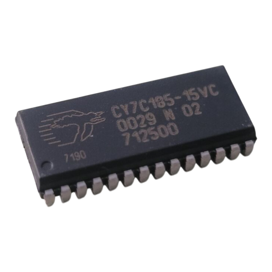
Truth Table Address Designators Address Address Name Function Number Ordering Information Speed (ns) Ordering Code CY7C185-15PC CY7C185-15SC CY7C185-15VC CY7C185-15VI CY7C185-20PC CY7C185-20SC CY7C185-20VC CY7C185-20VI CY7C185-25PC CY7C185-25SC CY7C185-25VC CY7C185-25VI CY7C185-35PC CY7C185-35SC CY7C185-35VC CY7C185-35VI Document #: 38-05043 Rev. *A Input/Output High Z High Z Data Out Data In High Z... -
Page 9: Package Diagrams
CY7C185 Package Diagrams 28-Lead (300-Mil) Molded DIP P21 51-85014-*B 28-Lead (300-Mil) Molded SOIC S21 51-85026-*A Document #: 38-05043 Rev. *A Page 9 of 11... - Page 10 Package Diagrams (continued) All product and company names mentioned in this document may be the trademarks of their respective holders. Document #: 38-05043 Rev. *A © Cypress Semiconductor Corporation, 2002. The information contained herein is subject to change without notice. Cypress Semiconductor Corporation assumes no responsibility for the use of any circuitry other than circuitry embodied in a Cypress Semiconductor product.
- Page 11 Document History Page Document Title: CY7C185 8K x 8 Static RAM Document Number: 38-05043 Issue REV. ECN NO. Date 107145 09/10/01 116470 09/16/02 Document #: 38-05043 Rev. *A Orig. of Change Description of Change Change from Spec number: 38-00037 to 38-05043 Add applications foot note to data sheet.
Need help?
Do you have a question about the 7C185-15 and is the answer not in the manual?
Questions and answers