Table of Contents
Advertisement
Quick Links
PCI-DSP01
User Manual
Version 1.0
ⓒ 2005 DAQ SYSTEM Co., Ltd. All rights reserved.
Microsoft® is a registered trademark; Windows®, Windows NT®, Windows XP®, Windows 7®, Windows 8®, Windows 10®
All other trademarks or intellectual property mentioned herein belongs to their respective owners.
Information furnished by DAQ SYSTEM is believed to be accurate and reliable, However, no responsibility is assumed by DAQ SYSTEM for its use, nor
for any infringements of patents or other rights of third parties which may result from its use. No license is granted by implication or otherwise under
any patent or copyrights of DAQ SYSTEM.
The information in this document is subject to change without notice and no part of this document may be copied or reproduced without the prior
written consent.
Advertisement
Table of Contents

Subscribe to Our Youtube Channel
Related Manuals for DAQ system PCI-DSP01


Summary of Contents for DAQ system PCI-DSP01
- Page 1 All other trademarks or intellectual property mentioned herein belongs to their respective owners. Information furnished by DAQ SYSTEM is believed to be accurate and reliable, However, no responsibility is assumed by DAQ SYSTEM for its use, nor for any infringements of patents or other rights of third parties which may result from its use. No license is granted by implication or otherwise under any patent or copyrights of DAQ SYSTEM.
-
Page 2: Table Of Contents
1-1 Product Features ------------------------------------------------------------------------ 2. PCI-DSP01 Features --------------------------------------------------------------------- 3. Installation Product Contents ------------------------------------------------------------------------ 3-2 Driver Installation ---------------------------------------------------------------------- 4. PCI-DSP01 Board Description 4-1 Layout ------------------------------------------------------------------------ 4-2 Function Description ---------------------------------------------------------------------- 4-3 Connector Pin Map ------------------------------------------------------------------------ 4-4 Expansion Connector Pin Map ---------------------------------------------------------- 4-5 Other Connector Pin Map... -
Page 3: Introduction
PCI slot of the PC. The figure below schematically shows the operation of the board. RS232C I/O BUS I/O Extention PCI-DSP01 Board [Figure 1-1. PCI-DSP01 Board Usage Example] As shown in [Figure 1-1], PCI-DSP01 is installed in the PCI slot in the PC to interface with external devices (RS232, User I/O Bus). - Page 4 PCI-DSP01 User’s Manual [Figure 1-2. PCI-DSP01 in action] [Figure 1-2] shows the connection when the PCI-DSP01 is interlocked with the actual equipment and tested. RS232 communication is performed through the 9Pin D-SUB connector on the left, and it is connected to the 44Pin DSUB connector at the bottom to show that I/O devices and I/O devices can...
-
Page 5: Product Features
PCI-DSP01 User’s Manual 1-1 Product Features Specification General -Point DSP chip Interface xtension connector -ns Instruction Cycle Time Functions -Bit On-Chip SRAM Software Windows 2000 SP4 / Windows XP SP1 Over Supported OS C6000, Code composer studio DSP Program Basic DSP firmware source, Sample application source... -
Page 6: Pci-Dsp01 Features
2. PCI-DSP01 Features As shown in the figure below, in the case of PCI-DSP01, the DSP chip is in charge of the overall control, and in the case of an external I/O bus, it can be changed using EPLD (XC9536XL). (Please refer to the drawing) 1. - Page 7 PCI-DSP01 User’s Manual [Figure 2-1. TMS320C6205 Function Block Diagram] FPGA core logic is programmed using JTAG, and the logic program is saved in FPGA Program Logic and loaded when power is applied.
- Page 8 PCI-DSP01 User’s Manual [TMS320C6205 DSP-CHIP Features] ♦ High-Performance Fixed-Point Digital Signal Processor (DSP) − TMS320C6205 − 5-ns Instruction Cycle Time − 200-MHz Clock Rate − Eight 32-Bit Instructions/Cycle − 1600 MIPS ♦ VelociTI Advanced-Very-Long-Instruction- Word (VLIW) TMS320C62x DSP Core − Eight Highly Independent Functional Units: −...
- Page 9 PCI-DSP01 User’s Manual ♦ 32-Bit/33-MHz Peripheral Component Interconnect (PCI) Master/Slave Interface Conforms to: PCI Specification 2.2 Power Management Interface 1.1 Meets Requirements of PC99 − PCI Access to All On-Chip RAM, Peripherals, and External Memory (via EMIF) − Four 8-Deep x 32-Wide FIFOs for Efficient PCI Bus Data Transfer −...
-
Page 10: Installation
3. RS232C Cable 3-2 Driver Installation To install your PCI-DSP01 board in your PC, follow the steps described in the document “How to install PCI DAQ Board” provided by DAQ System. The PCI-DSP01 board is completely Plug & Play. There are no switches or jumpers to set. Therefore you can install it easily. - Page 11 PCI-DSP01 User’s Manual If new hardware is found, Wizard will ask you to install the corresponding driver. For installation of the driver, select the item “Install from a list or specific location (Advanced)” and click “Next” as in the figure.
- Page 12 PCI-DSP01 User’s Manual If the installation is completely finished, you confirm it in the following ways. Do the following steps to show up the “Device Manager” window. [My Computer -> properties -> Hardware -> Device Manager -> Other Devices -> PCI-DSP01]...
- Page 13 PCI-DSP01 User’s Manual If you can see the “PCI-DSP01” at the “Other devices”, the driver installation is to have been over. (Check the red circle) Notice : After installation, you should re-boot the system for the proper operation.
-
Page 14: Pci-Dsp01 Board Description
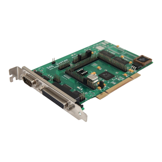
PCI-DSP01 User’s Manual 4. PCI-DSP01 Board Description Each important board function is briefly described. For detailed function information, please refer to the parts specification. 4-1 Layout RESE RS232C LED1 T/Rx I/O BUS EEPR Buffer LED2 EPLD Regulat FLASH [Figure 3-1. PCI-DSP01 Layout] The board has two LEDs to indicate the operation status. -
Page 15: Function Description
PCI-DSP01 User’s Manual 4-2 Function Description (1) DSP All of the board functions are controlled by the DSP Chip. (2) OSC The 40MHz clock supplies to the board. (3) EEPROM It saves a data of DSP chip functions setup when power up firstly. -
Page 16: Connector Pin Map
PCI-DSP01 User’s Manual 4-3 Connector Pin-out This section describes connectors and jumpers used in PCI-DSP01. The main connectors include a D-SUB 9pin connector for RS232C connection, and a D-SUB 44pin connector J1 for connecting P1 and external I/O. [Figure 4-2] shows the bracket that interfaces with the board and the connection connector. - Page 17 The figure below shows the pin map of the J1 connector of the board. All pin specifications are input/output through EPLD (XC9536XL), so please refer to the circuit diagram and EPLD program for details. I/O BUS [Figure 4-3. PCI-DSP01 J1 Connector Pin-out] [Table 1. J1 Connector] Name Description...
- Page 18 PCI-DSP01 User’s Manual RESET# Board Reset Output ETINP0 External Timer0 Input EFSX0 External FSX0 McBSP0 ECLKX0 External CLKX0 McBSP0 EDIR1 I/O Bus Direction1 EOE0 I/O Bus Output Enable0 Board GROUND DIO14 Digital I/O 14 DIO11 Digital I/O 11 DIO8 Digital I/O 8...
- Page 19 The figure below shows the pin map of the P1 connector of the board. All pin specifications are input/output based on the RS232 standard, so please refer to the circuit diagram for details. RS232C [Figure 4-4. PCI-DSP01 P1 Connector Pin-out] [Table 2. P1 Connector] Name Description...
-
Page 20: Expansion Connector Pin Map
PCI-DSP01 User’s Manual 4-4 Expansion Connector Pin-out In PCI-DSP01, the PIN (address, data, control, peripheral function signal) of the DSP chip can be connected externally so that all functions of the TMS320C6205 DSP chip can be tested. These connectors can be used by connecting them through J4, J6, and J8. - Page 21 PCI-DSP01 User’s Manual CLKS1 McBSP1 CLKX1 McBSP1 McBSP1 McBSP1 FSR1 McBSP1 None Maskable Interrupt FSX0 McBSP0 CLKR0 McBSP0 CLKS0 McBSP0 CLKX0 McBSP0 McBSP0 McBSP0 FSR0 McBSP0 Board GROUND Board GROUND INUM2 Interrupt Identification number 2 INUM3 Interrupt Identification number 3...
- Page 22 PCI-DSP01 User’s Manual External Data 1 External Data 2 External Data 3 External Data 4 External Data 5 External Data 6 External Data 7 External Data 8 External Data 9 ED10 External Data 10 ED11 External Data 11 ED12 External Data 12...
- Page 23 PCI-DSP01 User’s Manual Chip Enable 3 Board GROUND Board GROUND EA21 External Data 0 Chip Enable 1 EA19 External Address 19 EA20 External Address 20 EA17 External Address 17 EA18 External Address 18 EA15 External Address 15 EA16 External Address 16...
-
Page 24: Other Connector Pin Map
PCI-DSP01 User’s Manual 4-5 Other Connector Pin-out PCI-DSP01 has connectors and jumpers for setting board tests and functions and options at boot time. The functions of these connectors are as follows. VCC(+3.3V) JP1 Connector (Top View) JP1 uses the EPLD chip on the board to test the program. Do not use the board during normal operation. -
Page 25: Block Mode Option
J3 Connector (Top View) J3 is used by connecting DSP Emulator.. 4-6 Boot-Mode Option PCI-DSP01 has connectors and jumpers for setting board tests and functions and options at boot time. The functions of these connectors are as follows. Default Jumber... - Page 26 PLL0 PLL configuration 0 Pull-Up 10K Pull-up PLL1 PLL configuration 1 Pull-Up 10K Pull-up PLL2 PLL configuration 2 Note 1. For details, refer to the PCI-DSP01 reference manual 2. For details of each pin, refer to the TMS320C6205 User Manual...
-
Page 27: Test
PCI-DSP01 User’s Manual 5. Test In this chapter, we will conduct a functional test to learn whether the PCI-DSP01 board is faulty or not and how to use it briefly. 5-1 CDROM Folder Description The test is conducted using the software (driver, application program, DSP firmware) in the provided CD-ROM, and each folder of the CD-ROM will be briefly described. -
Page 28: Sample Program
PCI-DSP01 User’s Manual 5-2 Sample Program The CDROM provided with the board provides a sample program for use so that the board can be used easily. In order to test the sample program, the driver of the board must be installed first. - Page 29 PCI-DSP01 User’s Manual When the PCI-DSP01 board is installed in the PC, the board allocates and uses 3 memory areas (resources). Two are memory areas and one is mapped to I/O area, which can be checked in the sample program.
-
Page 30: Operation Test
PCI-DSP01 User’s Manual 5-3 Operation Test As shown in [Figure 1-2], after installing in an empty slot of the PC, turn on the power and install the driver. When power is applied, LED1 and LED2 are turned on to check whether power is supplied without any abnormality. -
Page 31: Dio Bus Input/Output Test
PCI-DSP01 User’s Manual If you press 0 to 3 in the communication program, a menu message is displayed on the communication program, and it can be confirmed that there is no abnormality in the communication. Press the “Memory0 Read” and “Memory1 Read” buttons to check whether the data is displayed as shown in [Figure 5-2], and press the “Write At”... -
Page 32: Appendix
PCI-DSP01 User’s Manual Appendix A-1 Board Size The external dimensions of the board are as follows. -
Page 33: Repair Regulations
(3) All DAQ SYSTEM products have a one-year warranty. -. The warranty period is counted from the date the product is shipped from DAQ SYSTEM. -. Peripherals and third-party products not manufactured by DAQ SYSTEM are covered by the manufacturer's warranty. -
Page 34: Reference
-- PCI Special Interest Group 3. How to install PCI DAQ Board -- DAQ system 4. AN201 How to build application using API -- DAQ system 5. PCI-DSP01 Reference Manual -- DAQ system 6. PCI-DSP01 API Manual -- DAQ system... - Page 35 PCI-DSP01 User’s Manual MEMO Contact Point Web sit : https://www.daqsystem.com Email : postmaster@daqsystem.com...
Need help?
Do you have a question about the PCI-DSP01 and is the answer not in the manual?
Questions and answers