Table of Contents
Advertisement
Quick Links
UM3100
User manual
SPC58EC-DIS discovery board
Introduction
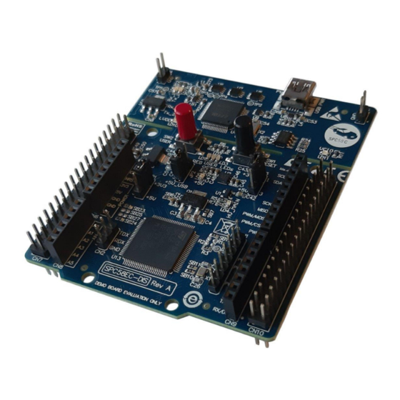
The SPC58EC-DIS is a low-cost development board to evaluate and develop applications with the microcontroller
SPC58EC80E3 in the eTQFP 100-pin package.
This document describes the hardware architecture of the SPC58EC-DIS discovery board and in which way the jumpers can be
set to enable specific functions.
Figure 1.
SPC58EC-DIS
Note:
Picture not contractual.
UM3100 - Rev 2 - June 2023
www.st.com
For further information contact your local STMicroelectronics sales office.
Advertisement
Table of Contents

Related Manuals for ST SPC58EC-DIS


Summary of Contents for ST SPC58EC-DIS
- Page 1 The SPC58EC-DIS is a low-cost development board to evaluate and develop applications with the microcontroller SPC58EC80E3 in the eTQFP 100-pin package. This document describes the hardware architecture of the SPC58EC-DIS discovery board and in which way the jumpers can be set to enable specific functions.
-
Page 2: Overview
32-bit power architecture technology CPU 180 MHz, 1088 KB 4224 KB (4096 KB code flash memory + 128 KB data flash memory) 384 KB SRAM in an eTQFP100 package. The SPC58EC-DIS allows full access to peripherals such as DSPI, LINFlexD, ISO CAN-FD. The new features satisfy the ASIL-B requirements. -
Page 3: Figure 3. Spc58Ec-Dis Bottom View
UM3100 Overview Figure 3. SPC58EC-DIS bottom view UM3100 - Rev 2 page 3/31... -
Page 4: License Agreement
Attention: This evaluation board only offers limited features for evaluating ST products. It has not been tested for use with other products and is not suitable for any safety or other commercial or consumer application. This evaluation board is otherwise provided “AS IS”... -
Page 5: Handling Precautions
UM3100 Handling precautions Handling precautions Please take care to handle the package content in order to prevent electrostatic discharge. Before the EVB is used or the power is applied, please fully read the following sections on how to correctly configure the board. Failure to correctly configure the board may cause irreparable component, MCU or EVB damage. -
Page 6: Hardware Description
UM3100 Hardware description Hardware description Power supply section The SPC58EC-DIS can be supplied by using some DC sources, setting some jumpers properly: • by the host PC through the USB cable (5 V; this is the default configuration) • by an external source connected to the VIN pin (CN6 pin 8, CN7 pin 24) (7÷12V). The maximum input voltage level is limited by the thermal dissipation of the linear regulators. -
Page 7: Microcontroller Power Management
UM3100 Microcontroller power management Figure 5. 5 V regulator (external PSU) and 5 V selector (JP2) JP-B2 BLACK BRIDGE LD1117S50TR 5V_USB 5V_USB TAB (Output) 5V_Reg Input Output 3 Male Pins Default 2-3 100n 100n Green Figure 6. 3.3 V voltage regulator and 3.3 V selector (SB26) LD39050PU33R SB26 Closed... -
Page 8: Table 2. Power Domains Jumper Configuration
VDD_HV_IO_FLA configuration jumper: Closed Bottom layer – C3 • Open: VDD_HV_IO_FLA connected to VDD_HV_IO • Closed: VDD_HV_IO_FLA unconnected 1. Refer to the Figure 18. SPC58EC-DIS top layer. 2. Refer to the Figure 19. SPC58EC-DIS bottom layer. UM3100 - Rev 2 page 8/31... -
Page 9: Integrated Programmer/Debugger
The integrated debugger SW is accessible via ST's free integrated development environment, SPC5-STUDIO (www.st.com/spc5studio). To download the debugger software and to activate a license refer to the PLS website. A JTAG port allows connecting further HW/SW tools to program and debug the microcontroller(s). U106 can be configured to establish a serial communication port;... -
Page 10: Figure 11. Level Shifters Of The Pls Integrated Programmer/Debugger
UM3100 Integrated programmer/debugger The following figure shows the level shifters of the PLS integrated programmer/debugger circuitry. Figure 11. Level shifters of the PLS integrated programmer/debugger LVDD VCIO VCCA VCCB TCK_O TCK_USB LVDD TDI_O TDI_USB A→B VCIO SN74LVC2T45DCTR GND_USB LVDD VCIO VCCA VCCB TMS_DIR... -
Page 11: Crystal Oscillator
Closed: EXTAL connected to 40 MHz crystal oscillator (X1) XTAL jumper configuration: SB11 Closed Top layer – C4 • Open: XTAL not connected • Closed: XTAL connected to 40 MHz crystal oscillator (X1) 1. Refer to the Figure 18. SPC58EC-DIS top layer. UM3100 - Rev 2 page 11/31... -
Page 12: Reset Circuit
NRST jumper configuration: SB19 Closed Bottom layer – B3 • Open: NRST not connected • Closed: NRST connected to the pin 3 of CN6 connector 1. Refer to the Figure 19. SPC58EC-DIS bottom layer. UM3100 - Rev 2 page 12/31... -
Page 13: User Leds - User Button
Pins connected to user LEDs and user pushbutton User LEDs and user pushbutton Position Top layer – B2 Top layer – B2 PD13 Top layer – B2 Top layer – B2 1. Refer to the Figure 18. SPC58EC-DIS top layer. UM3100 - Rev 2 page 13/31... -
Page 14: Connectors
Top layer – A4 Arduino UNO-R3 digital PWM (D7÷D0) Top layer – D3 D4 1. Refer to the Figure 18. SPC58EC-DIS top layer. The following table shows the pinout of the Arduino UNO-R3 digital PWM (from D15 to D8) (CN5) connector. Table 8. -
Page 15: Extended Connectors (I/O Headers)
Top layer – A2 A3 A4 CN10 Extended connector (I/O headers) Top layer – D2 D3 D4 1. Refer to the Figure 18. SPC58EC-DIS top layer. The following table shows the pinout of the extended connector (CN7). Table 13. Extended connector (CN7) connector pinout... -
Page 16: Table 14. Extended Connector (Cn10) Connector Pinout
UM3100 Connectors Extended connector (CN7) uC Port Not connected Not connected Not connected VDD_HV_IO_MAIN PD14 NRST PC[0] PE[0] PC[7] PC[6] PC[5] PC[4] Not connected PE[3] PG[12] PE[1] PG[11] PD[13] PD[10] VDD_HV_IO_MAIN PB[10] PE[2] PB[9] PD[12] PB[8] The following table shows the pinout of the extended connector (CN10). Table 14. - Page 17 UM3100 Connectors Extended connector (CN10) μC Port VDD_HV_ADC Not connected PD[6] PA[10] PD[7] PA[11] PF[13] PD[0] PA[4] PA[0] PA[1] PA[2] Not connected PE[7] PB[11] PE[5] PB[2] PE[6] PB[3] PE[9] PB[1] PD[4] PD[5] PD[11] PA[3] Not connected PA[15] Not connected UM3100 - Rev 2 page 17/31...
-
Page 18: Uart Connector
UM3100 Connectors 4.7.3 UART connector The following table shows the pinout of the UART connector (CN2). Table 15. UART connector pinout CN2 pin Function/signal SB23 closed SB25 open SB23 open SB25 closed SB24 closed PA15 SB27 open SB24 open SB27 closed 4.7.4 JTAG connector The following table shows the pinout of the JTAG connector (CN1). -
Page 19: Layout Overview
UM3100 Layout overview Layout overview Figure 18. SPC58EC-DIS top layer UM3100 - Rev 2 page 19/31... -
Page 20: Figure 19. Spc58Ec-Dis Bottom Layer
UM3100 Layout overview Figure 19. SPC58EC-DIS bottom layer UM3100 - Rev 2 page 20/31... -
Page 21: Bom
UM3100 Table 17. Bill of material Item Value Description Footprint C1, C5, C8, C1608X7R1C105K080AC - SMD multilayer C11, C14, C46, 1 μF ceramic capacitor, 1 µF, 16 V, 0603 [1608 metric], 0603C ±10%, X7R, C series TDK C2, C6, C9, C12, C15, C18, C20, C22, C24, C28, C30, C32,... - Page 22 UM3100 Item Value Description Footprint 21 LD4, LD8, LD9 Led red LED uni-color red 625 nm 2-pin chip LED 0603D_R USB-MINI_B CONN USB MINI B 67503-1020 BCP68-25 SMD NPN transistor medium power SOT223_BCE_T Resistor thick film 0603 10 kΩ 1% 1/10W R1, R2 RES 0603 ±100 ppm/C molded SMD punched carrier T/R...
- Page 23 UM3100 Item Value Description Footprint USBLC6 series 2 channel 5.25 V SMT uni- USBLC6-2P6 SOT666 directional ±15 kV ESD protection-SOT-666 U9, U11 Single-bit dual-supply bus transceiver SC-70 IC REG LDO 3.3V 0.8A SOT223 SOT-223 1 KB (x16) serial microwire bus EEPROM with SO-8 block protection 100_LQFP_14X14X1.6_EXP-...
-
Page 24: Schematics
Schematics Figure 20. SPC58ECx MCU U13A SPC58EC80E3 U13B SPC58EC80E3 Port A VSS_HV_ADR_S VDD_HV_ADR_S PA[0] PI[1] VDD_HV_ADC PA[1] PI[2] VDD_HV_ADC PA[2] PI[3] VSS_HV_ADV_S VDD_HV_ADV_S PA[3] PI[4] PA[4] PI[6] JCOMP PA[5] PI[7] GND_HV_ADx_S PA[6] Port A PA[7] VDD_HV_OSC Closed Port M VSS_HV_OSC VDD_HV_OSC PA[8] PA[9]... - Page 25 Figure 21. SPC58ECx connectors SB13 Open SB14 Open CN10 Header 19X2 Header 19X2 E3V3 Header 10X1_Female PA12 PA13 PC10 PC11 PE10 PE12 Header 8X1_Female PE11 VDD_HV_IO_MAIN VDD_HV_ADC AVDD AVDD PD15 IOREF VDD_HV_IO_MAIN PA10 NRST DSPI 1 CLK 11 12 PA11 DSPI 1 SIN-MISO 11 12 13 14...
-
Page 26: Figure 22. Spc58Ecx Usb Section
Figure 22. SPC58ECx USB section LVDD LVDD VCIO VCCA VCCB LVDD TCK_O TCK_O TCK_USB VCCIO ADBUS0 TDI_O TDI_O A→B TDI_USB VCCIO ADBUS1 TDO_I VCIO VCIO VCCIO ADBUS2 VDD_HV_IO_MAIN TMS_IO 60Ohm@100MHz VCCIO ADBUS3 V_CORE TMS_IO SN74LVC2T45DCTR ADBUS4 RTCK_I GND_USB 1.8V VCORE ADBUS5 ADBUS5 VCORE... -
Page 27: Revision History
UM3100 Revision history Table 18. Document revision history Date Revision Changes 22-Nov-2022 Initial release. Updated Figure 13. Jumpers configuration of PLS integrated programmer/debugger, 06-Jun-2023 Table 11. Arduino UNO-R3 digital PWM (from D7 to D0) (CN9) pinout, Table 15. UART connector pinout, Figure 21. -
Page 28: Table Of Contents
UM3100 Contents Contents Overview ................2 License agreement . - Page 29 UM3100 List of tables List of tables Table 1. Power source and jumpers configuration........... . 6 Table 2.
- Page 30 SPC58EC-DIS bottom layer ........
- Page 31 ST’s terms and conditions of sale in place at the time of order acknowledgment. Purchasers are solely responsible for the choice, selection, and use of ST products and ST assumes no liability for application assistance or the design of purchasers’...
Need help?
Do you have a question about the SPC58EC-DIS and is the answer not in the manual?
Questions and answers