Table of Contents
Advertisement
Quick Links
UM2462
User manual
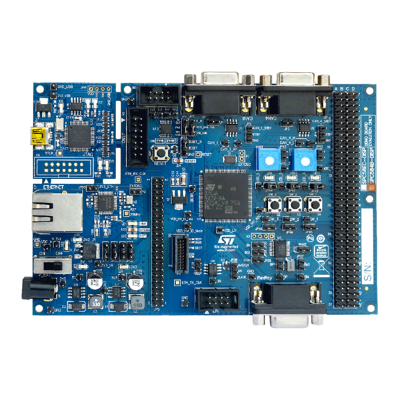
SPC584B-DISP discovery board
Introduction
The SPC584B-DISP discovery plus board is a development board to evaluate and develop applications with the microcontroller
SPC584B70E5 in eTQFP144 package.
This document describes the hardware architecture of the board and how it is possible to enable specific functions through the
configuration of the jumpers.
UM2462 - Rev 3 - March 2022
www.st.com
For further information contact your local STMicroelectronics sales office.
Advertisement
Table of Contents

Related Manuals for ST SPC584B-DISP


Summary of Contents for ST SPC584B-DISP
- Page 1 SPC584B-DISP discovery board Introduction The SPC584B-DISP discovery plus board is a development board to evaluate and develop applications with the microcontroller SPC584B70E5 in eTQFP144 package. This document describes the hardware architecture of the board and how it is possible to enable specific functions through the configuration of the jumpers.
-
Page 2: Overview
Overview The several interfaces including Ethernet controller, CAN-FD, LIN and UART, ADC, and JTAG port make the SPC584B-DISP an excellent tool to evaluate the microcontroller as well as to develop and then debug applications. An integrated programmer debugger (supported PLS) allows debugging and programming the microcontroller. -
Page 3: License Agreement
Attention: This evaluation board only offers limited features for evaluating ST products. It has not been tested for use with other products and is not suitable for any safety or other commercial or consumer application. This evaluation board is otherwise provided “AS IS”... -
Page 4: Handling Precautions
UM2462 Handling precautions Handling precautions Please take care to handle the package content in order to prevent electrostatic discharge. Before the EVB is used or power is applied, please fully read the following sections on how to correctly configure the board. Failure to correctly configure the board may cause irreparable component, MCU or EVB damage. UM2462 - Rev 3 page 4/25... -
Page 5: Hardware Overview
UM2462 Hardware overview Hardware overview Power supply section The input voltage level is 12 V , the output voltage is set to 5 V and 3.3 V. Figure 2 Figure 3 show the buck converters used to generate 5 V and 3.3 V respectively. Figure 2. -
Page 6: Microcontroller Power Management
If the external programmer does not work properly, the jumpers SB8÷SB14 must be removed (open). It is suggested to perform some tests before removing the jumpers SB8÷SB14. The SPC584B-DISP comes with the integrated programmer enabled (all solder jumpers from SB8 to SB14 are present). -
Page 7: Crystal Oscillator And Reset
UM2462 Crystal oscillator and reset Crystal oscillator and reset Figure 6 shows the external oscillator circuit; the frequency is 40 MHz. By setting SB2, SB3 (open) and SB3 (closed) it is possible to drive the EXTAL pin with an external clock. Figure 6. -
Page 8: Rs232 And Lin
UM2462 RS232 and LIN RS232 and LIN Two serial communication channels are available; U10 is a dual RS232 driver and receiver (see Figure Figure 8. RS232 section Rx_B SCI_0_RX SCI_ChB Tx_B SCI_0_TX Default: 1-2 R1_OUT TP26 TP27 VDD_HV_IO_Main VDD_HV_IO_Main TXD_USB SCI_RX_Sel R1 IN R1 OUT... -
Page 9: User Interface (Pushbuttons, Leds And Trimmers)
UM2462 User interface (pushbuttons, LEDs and trimmers) User interface (pushbuttons, LEDs and trimmers) In the board three LEDs and three push-buttons are present and they are suitable for user purposes (see Figure 10). Figure 10. User pushbutton and LEDs VDD_HV_IO_Main TP41 TP38 SW_2... - Page 10 UM2462 Extended connectors (I/O headers) X9 pinA Function/Port pinA X9 pinB Function/Port pinB PE10_LIN_0_RXD PD11_eMIOS0-UC21 PE9_eMIOS0-UC9 PK14_GPIO174 RESET PE1_eMIOS0-UC12 PA12_DSPI2-CS0 PH0_GPIO112 PB9_DSPI2-SIN PB10_DSPI2-SOUT PF7_CAN4sys1-TX PF6_CAN4sys1-RX PG1_GPIO97 PI9_GPIO137 PD1_I2C-SDA PD2_I2C-SCL PA11_CAN1sys0_RX PA10_CAN1sys0_TX PI8_GPIO136 PA0_LIN4_RXD PF11_SW_User_1 PF0_GPIO80 PF12_SW_User_2 PF13_SW_User_3 PG14_GPIO110 PF1_eMIOS1-UC1 PC14_eMIOS-UC27 PI3_ADC-AN39 PI5_ADC-AN41 PI6_ADC-AN49...
- Page 11 UM2462 Extended connectors (I/O headers) X9 pinC Function/Port pinC X9 pinD Function/Port pinD PB4_ADC_User_2 PK0_GPIO160 PD14_LIN_6_TXD PI1_eMIOS0-UC4 PF8_LED_User_1 PE13_eMIOS0-UC23 PF9_LED_User_2 PF10_LED_User_3 PA2_CAN2sys0_TX PA1_CAN2sys0_RX PE6_CAN0sys0_RX PE5_CAN0sys0_TX PE7_LIN_1_TXD PF2_EIRQ6 PB11_FCCU-F0 PC2_FCCU-F1 PF14_GPIO94 PA3_DSPI2_SOUT PA3_eMIOS0-UC28 PC7_eMIOS0-UC3 PD12_eMIOS0-UC14 PK1_GPIO161 PH1_GPIO113 PI7_ADC-AN50 PG2_ADC-AN25 PG11_ADC-AN57 PI4_ADC-AN40 PG6_ADC-AN44 PG9_ADC-AN53 PB6_ADC-AN48...
-
Page 12: Pcb Layout
PCB layout Figure 12. SPC584B-DISP - PCB top side... -
Page 13: Schematics
Schematics Figure 13. Power supply 3V3_LR TP18 A5973AD SB24 V_Ext Closed 15uH/2A JP34 COMP SYNC 5,6kΩ VDD_HV_IO_Main VDD_HV_IO_Main 10uF/50V 100nF/50V 22nF/50V 3,3kΩ 100nF/50V 330uF/10V Header 3x1 220pF/50V TP19 JP35 STPS340U 4,7kΩ VDD_HV_IO_Flex VDD_HV_IO_Flex Header 3x1 JP36 TP20 VDD_HV_ADC VDD_HV_ADC A5973AD SB25 Header 3x1 V_Ext... - Page 14 Figure 14. USB and debugger 3V3_USB TCK_O VCCIO ADBUS0 USB - Serial Communication Channel TDI_O VCCIO ADBUS1 Direction A->B TDO_I VCCIO ADBUS2 FT2232H->Micro TMS_IO TP33 VCCIO ADBUS3 3V3_USB VCIO TMS_IO VCCA VCCB Not Assembled ADBUS4 3V3_USB RTCK_I VCORE ADBUS5 USB_TX TXD_USB V_CORE 1.8V...
- Page 15 Figure 15. JTAG and reset USB_TDI Closed USB_TDI USB_TDO Closed USB_TDO USB_TCK SB10 Closed USB_TCK USB_TMS SB11 Closed USB_TMS USB_SRST# SB12 Closed USB_SRST# USB_TRST# SB13 Closed USB_TRST# SB14 Closed EVTI RESET RESET VDD_HV_IO_Main VDD_HV_IO_Main VDDE7 GND RDY JCOMP Not Assembled 10kΩ...
- Page 16 Figure 16. RS232 and LIN Rx_B SCI_0_RX SCI_ChB Tx_B SCI_0_TX Default: 1-2 R1_OUT TP26 TP27 VDD_HV_IO_Main VDD_HV_IO_Main TXD_USB SCI_RX_Sel R1 IN R1 OUT R2 IN R2 OUT Rx_A T1_IN SCI_4_RX T1 IN T1 OUT SCI_ChA Tx_A SCI_4_TX T2 IN T2 OUT TP28 TP29 Default: 1-2...
- Page 17 Figure 17. CAN and ISO CAN-FD V_Ext VDD_HV_IO_Main VDD_HV_IO_Main CAN_1_H CAN_1_L 0Ω CAN1_TX CAN1sys0_TX CANH 22Ω CAN_1_L CANL CAN_1_H CAN1_RX CAN1sys0_RX 22Ω 47pF/16V 47pF/16V 60,4Ω 60,4Ω 100nF/50V 10kΩ STBY D-SUB 9 WAY FEMALE Closed CAN_1_STBY 100nF/50V CAN_1_STBY MCP2562FD 4,7nF/16V 4,7nF/16V 100Ω...
- Page 18 Figure 18. Ethernet 3V3_ETH 220Ω 220Ω 220Ω 3V3_ETH JP50 SB23 SB22 SB21 Open Open Open Closed C132 C133 LED_LINK 10uF/16V 100nF/50V LED_ACT LED_SPEED 3V3_ETH 3V3_ETH 3V3_ETH Not Assembled ETH_TX_CLK 4,7kΩ TP10 1,5kΩ Not Assembled 3V3_ETH 4,7kΩ Not Assembled Yellow SB20 K_LED Y A_LED Y Closed...
- Page 19 Figure 19. User interface VDD_HV_ADC VDD_HV_ADC TP36 TP37 C127 ADC_2 ADC_1 100nF/50V JP42 ADC_User_1 R102 ADC_User_1 10kΩ Closed JP43 ADC_User_2 R103 ADC_User_2 10kΩ Closed C128 C129 100nF/50V 100nF/50V USER - ADC Evaluation TP38 LED_2 TP39 TP40 VDD_HV_IO_Main TP41 VDD_HV_IO_Main LED_1 LED_3 SW_2 TP42...
- Page 20 PG6_ADC-AN44 PG9_ADC-AN53 PB6_ADC-AN48 PB7_ADC-AN47 PE0_ADC-AN11 PG12_ADC-AN58 PD8_ADC-AN92 PE3_ADC-AN17 PG10_ADC-AN55 PL8_ADC-AN5 PI2_eMIOS0-UC5 PD5_DSPI0-SOUT PE15_DSIP0-SIN PE2__ADC-AN13 SPI0_SOUT SPI0_SIN PM14_GPIO206 PE8_DSIP0-CS0 PD4_DSPI0-SCK LED 9 SPI0_CS0 SPI0_SCK PG15_LIN1-TXD PM2_GPIO194 LIN1_RX LED 10 V_EXT_P V_EXT_P V_Ext HEADER 4X37 GPIO_4x36 JP40 V_EXT_P V_Ext Close logo\ST-logo_201 2.jpg...
- Page 21 Figure 21. Microcontroller power management Pin 42 VDD_HV_ADC Pin 44 VDD_HV_ADC VSS_HV_ADR_C VDD_HV_ADR_C VDD_HV_ADC VSS_HV_ADV_S VDD_HV_ADV_S A_GND OSC & JTAG (3.3V or 5V) VSS_HV_OSC VDD_HV_JTAG_OSC GND_OSC VDD_HV_IO_W0 VDD_HV_IO0_S0 VDD_HV_IO_Main I/O (3.3V - 5V) VDD_HV_IO_Main Pin 83 Pin 23 Pin 59 Pin 78 Pin 115 Pin 142...
- Page 22 Figure 22. Microcontroller IO signal PA0_LIN4-RXD PE0_ADC-AN11 SCI_4_RX PA[0] eMIOS0-UC14 LIN1-TXD DSPI6-CS0 PE[0] eMIOS0-UC11 DSPI3-CS2 ADC-AN11 ETH_MDC PA1_CAN2sys0_RX PE1_eMIOS0-UC12 PA[1] eMIOS 0 UC11 DSPI7-CS0 LIN1-TDX PE[1] LIN5-TXD eMIOS0-UC12 DSPI3-CS1 ADC-AN12 PA2_CAN2sys0_TX PE2__ADC-AN13 PA[2] LIN1-TXD eMIOS0 UC10 CAN2sys0-TX PE[2] DSPI3-CS3 eMIOS-UC13 DSPI3-SOUT ADC-AN13 PA3_DSPI2_SOUT PE3_ADC-AN17 DSPI2_SOUT...
-
Page 23: Revision History
UM2462 Revision history Table 3. Document revision history Date Revision Changes 04-Sep-2018 Initial release. 02-Mar-2020 Minor text changes. Added Section 2 License agreement Section 3 Handling precautions. Removed "FlexRay" section. Added Figure 8. RS232 section and updated Figure 9. LIN section. -
Page 24: Table Of Contents
UM2462 Contents Contents Overview ................2 License agreement . - Page 25 ST’s terms and conditions of sale in place at the time of order acknowledgment. Purchasers are solely responsible for the choice, selection, and use of ST products and ST assumes no liability for application assistance or the design of purchasers’...
Need help?
Do you have a question about the SPC584B-DISP and is the answer not in the manual?
Questions and answers