
Related Manuals for ADLINK Technology VPX3020 Series


Summary of Contents for ADLINK Technology VPX3020 Series
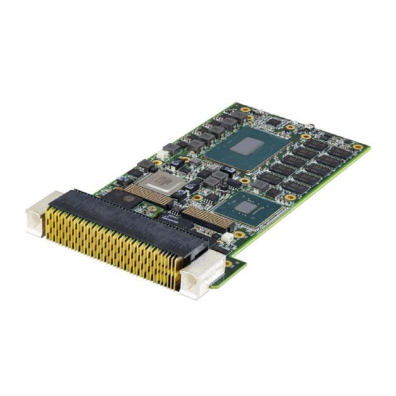
- Page 1 VPX3020 Series Performance Rugged Conduction Cooled ® ® 3U VPX Intel Xeon Processor E Processor Blade User’s Manual Manual Rev.: Revision Date: August 25, 2022 Part No: 50M-00050-1000...
- Page 2 Revision History Revision Release Date Description of Change(s) 2022/08/25 Initial release Revision History...
-
Page 3: Preface
VPX3020 Preface Copyright © 2022 ADLINK Technology, Inc. This document contains proprietary information protected by copy- right. All rights are reserved. No part of this manual may be repro- duced by any mechanical, electronic, or other means in any form without prior written permission of the manufacturer. - Page 4 California Proposition 65 Warning WARNING: This product can expose you to chemicals including acrylamide, arsenic, benzene, cadmium, Tris(1,3-dichloro-2-propyl)phosphate (TDCPP), 1,4-Diox- ane, formaldehyde, lead, DEHP, styrene, DINP, BBP, PVC, and vinyl materials, which are known to the State of California to cause cancer, and acrylamide, benzene, cadmium, lead, mercury, phthalates, toluene, DEHP, DIDP, DnHP, DBP, BBP, PVC, and vinyl materials, which are known to the State of California to cause...
-
Page 5: Table Of Contents
VPX3020 Table of Contents Revision History..............ii Preface ..................iii List of Figures ............... vii List of Tables................ix 1 Introduction ................ 1 Overview................1 Features................1 Block Diagrams..............2 Model Number Decoder - Processor Blade ......3 Package Contents ............... 5 2 Specifications .............. - Page 6 3.13 UART NCT5104..............18 3.14 TPM ................... 18 3.15 XMC Site................18 4 VPX3020 Board Interfaces ..........19 VPX3020 Board Layout ............. 19 VPX3020 Mechanical Dimensions........20 VPX3020 Connector Pin Assignments ......22 Status LEDs ............... 27 5 VPX-R3020 RTM ..............29 Connector Allocation............
-
Page 7: List Of Figures
VPX3020 List of Figures Figure 1-1: VPX3020 Functional Block Diagram........ 2 Figure 4-1: VPX3020 Top Side Layout ..........19 Figure 4-2: VPX3020 Bottom Side Layout ........19 Figure 4-3: VPX3020 Conduction-Cooled Mechanical Dimensions. 20 Figure 4-4: VPX3020 Air-Cooled Mechanical Dimensions....21 Figure 4-5: VPX3020 Front View ............. - Page 8 This page intentionally left blank. viii List of Figures...
-
Page 9: List Of Tables
VPX3020 List of Tables Table 1-1: VPX3020 SKU Table ............4 Table 2-1: VPX3020 Blade Specifications ........7 Table 2-2: VPX-R3020 RTM Specifications........9 List of Tables... - Page 10 This page intentionally left blank. List of Tables...
-
Page 11: Introduction
VPX3020 Introduction 1.1 Overview The VPX3020 Series is a 3U VPX processor blade based on the Intel® Xeon® Processor E-2254ML (formerly "Coffee Lake-H Refresh"), supporting DDR4-2666 ECC soldered memory up to 16GB. For storage, the VPX3020 provides a high endurance sol- dered 32GB SLC SSD. -
Page 12: Block Diagrams
1.3 Block Diagrams DDR4 8Gb + ECC 2666MT/s DDR4 8Gb + ECC 2666MT/s XMC SKU PCIe SKU Figure 1-1: VPX3020 Functional Block Diagram Introduction... -
Page 13: Model Number Decoder - Processor Blade
VPX3020 Model Number Decoder - Processor Blade VPX3020/2254/M16/S32/XMC-R2 (A) CPU Code E-2254ML = Intel® processor E-2254ML, 4 cores, 25W (B) Memory Size Code M16 = 16GB DDR4-2666 ECC soldered SDRAM (C) SATA NAND Flash Size Code S32 = SLC NAND flash 32GB SATA 6Gb/s via add-on card ... - Page 14 VPX3020 SKU Table Function XMC Version PCIe Version PCIe x8 Gen3 (or 2x PCIe x4) w/ rear IO to P2 (X8d+X12d) 1x 1000BASE-T + 2x 1000BASE-BX to P1 Ethernet PCIe Switch downstream port to P1 Station 0 port: 2 x4 Station 1 port: 1 x4 Express 2x PCIe Gen3 x4 to P2...
-
Page 15: Package Contents
VPX3020 1.5 Package Contents The VPX3020 is packaged with the following components. If any of the items on the contents list are missing or damaged, retain the shipping carton and packing material and contact the dealer for inspection. Please obtain authorization before returning any prod- uct to ADLINK. - Page 16 This page intentionally left blank. Introduction...
-
Page 17: Specifications
VPX3020 Specifications 2.1 VPX3020 Blade Specifications VITA • VITA 46.0 VPX Base Standard Standards • VITA 46.4 PCI Express on VPX Fabric Connector • VITA 46.6 Gigabit Ethernet Control Plane on VPX • VITA 46.9 PMC/XMC/Ethernet Signal Mapping to 3U/6U VPX •... - Page 18 Serial • 1x RS-232/422 (COM1) to P2 • 1x RS-232/422/485 (COM2) to P2 Note: RS-422 on COM1 & RS-485 on COM2 are not simultaneously supported. • To P1 • Infineon TPM version 2.0 LEDs • Status LEDs on front and rear Reset Button •...
-
Page 19: Vpx-R3020 Rtm Specifications
VPX3020 2.2 VPX-R3020 RTM Specifications Ethernet • 2x 1000BASE-BX via RP1 • 1x 1000BASE-T via RP1 Graphics • 1x DisplayPort signal via RP1 SATA • 1x SATA 6Gb/s via RP1 (7 pin vertical SATA connector) • 1x USB 3.0 (backwards compatible) via RP1 Serial •... -
Page 20: Power Consumption
2.3 Power Consumption This section provides information on the power consumption of the VPX3020 Series when using Intel® Xeon® E-2254ML processors with Dual Channel 8GB DDR4-2666 soldered memory and SATA SSD. The VPX3020 is pow- ered by 5V and 3.3V. Windows 10 Typical power consumption was measured running BurnInTest at 100% loading. - Page 21 VPX3020 Processor Xeon® E-2254ML (1.7 GHz) Windows Max Loading mode, EIST Disabled Package Power reading (TAT) 24.98W Package Temperature reading (TAT) 72°C CPU DTS reading (TAT) 72°C CPU frequency reading (TAT) 1287MHz 3.3V (A) 5V (A) 6.45 Power Cons. (W) 41.16 Specifications...
- Page 22 This page intentionally left blank. Specifications...
-
Page 23: Functional Description
VPX3020 Functional Description The following sections describe the VPX3020 features and functions. 3.1 Processors The Intel® Xeon® E Processor is a 64-bit, multi-core processor built on 14-nanometer process technology. The processor is designed for a two-chip platform consisting of a processor and chipset. - Page 24 Supported Technologies Intel® Virtualization Technology for Directed I/O (Intel® VT-d) Intel® Virtualization Technology (Intel® VT-x) Intel® VT-x with Extended Page Tables (EPT) Intel® Hyper-Threading Technology (Xeon® E-2254ML only) Intel® 64 Architecture Execute Disable Bit Intel®...
-
Page 25: Intel® Turbo Boost Technology
VPX3020 3.2 Intel® Turbo Boost Technology Intel Turbo Boost Technology is a feature that allows the processor to opportunistically and automatically run faster than its rated operating core and/or render clock frequency when there is suffi- cient power headroom, and the product is within specified temper- ature and current limits. -
Page 26: Chipset
3.3 Chipset The Mobile Intel® C240 Series Chipset provides extensive I/O support. Functions and capabilities include: PCI Express Base Specification, Revision 3.0 ACPI Power Management Logic Support, Revision 4.0a Interrupt controller and timer functions Integrated Serial ATA host controller 3.2, supports data ... -
Page 27: System Management Bus
VPX3020 3.6 System Management Bus The PCH provides a System Management Bus (SMBus) Specifi- cation Version 2.0 compliant Host Controller as well as an SMBus Slave Interface. The PCH provides a mechanism for the processor to initiate communications with SMBus peripherals (slaves) as well as I2C compatible devices. -
Page 28: Graphics
2.0 and features Low Pin Count (LPC) interface. 3.15 XMC Site The VPX3020 Series supports one XMC site for rear I/O expan- sion. The XMC site provides a x8 PCI Express Gen 3.0 lane. Jn2 rear XMC I/O connector is compliant to VITA 46.9, X8d+X12d. -
Page 29: Vpx3020 Board Interfaces
VPX3020 VPX3020 Board Interfaces This chapter illustrates the board layout, connector pin assign- ments, and jumper settings to familiarize users with the VPX3020. 4.1 VPX3020 Board Layout DDR4 ECC Memory Chipset SATA Card Connector PCIe Switch Super IO Figure 4-1: VPX3020 Top Side Layout DDR4 ECC Memory BIOS1 SPI ROM BIOS2 SPI ROM... -
Page 30: Vpx3020 Mechanical Dimensions
4.2 VPX3020 Mechanical Dimensions Conduction-Cooled Version Dimensions in mm Figure 4-3: VPX3020 Conduction-Cooled Mechanical Dimensions VPX3020 Board Interfaces... -
Page 31: Figure 4-4: Vpx3020 Air-Cooled Mechanical Dimensions
VPX3020 Air-Cooled Version 21.29 Dimensions in mm Figure 4-4: VPX3020 Air-Cooled Mechanical Dimensions VPX3020 Board Interfaces... -
Page 32: Vpx3020 Connector Pin Assignments
4.3 VPX3020 Connector Pin Assignments XMC Connectors JN15 Connector Pin Definition (Primary) PET0p0 PET0n0 3.3V PET0p1 PET0n1 VPWR TRST# RESET# PET0p2 PET0n2 3.3V PET0p3 PET0n3 VPWR PULL UP PET0p4 PET0n4 3.3V PET0p5 PET0n5 VPWR 12V_AUX PET0p6 PET0n6 3.3V PET0p7 PET0n7 VPWR -12V_AUX VPWR... - Page 33 VPX3020 J16 Connector Pin Definition (X8d+X12d) XMC_A1+ XMC_B1- XMC_D1+ XMC_E1- XMC_A3+ XMC_B3- XMC_D3+ XMC_E3- XMC_A5+ XMC_B5- XMC_D5+ XMC_E5- XMC_A7+ XMC_B7- XMC_D7+ XMC_E7- XMC_A9+ XMC_B9- XMC_D9+ XMC_E9- XMC_A11+ XMC_B11- XMC_D11+ XMC_E11- XMC_A13+ XMC_B13- XMC_D13+ XMC_E13- XMC_A15+ XMC_B15- XMC_D15+ XMC_E15- XMC_A17+ XMC_B17- XMC_D17+ XMC_E17- XMC_A19+...
- Page 34 VPX Connectors P0 Connector 3.3V 3.3V 3.3V 3.3V 3.3V 3.3V IPM1_CLK IPM1_DAT N12V_AUX SYSRESET# NVMRO 3.3V_AUX IPM2_CLK IPM2_DAT P12V_AUX IPMB_ IPMB_ IPMB_ IPMB_ IPMB_ JTCK JTDO JTDI JTMS JTRST-L H_CLK_P0_ H_CLK_P0_ REF_CLK- REF_CLK+ 100M_N/ 100M_P/ RES_BUS- RES_BUS+ VPX3020 Board Interfaces...
- Page 35 VPX3020 P1 Connector GDISC1# L0-TX- L0-TX+ L0-RX- L0-RX+ L1-TX- L1-TX+ L1-RX- L1-RX+ P1_VBAT L2-TX- L2-TX+ L2-RX- L2-RX+ L3-TX- L3-TX+ L3-RX- L3-RX+ SYSCON# L4-TX- L4-TX+ L4-RX- L4-RX+ L5-TX- L5-TX+ L5-RX- L5-RX+ L6-TX- L6-TX+ L6-RX- L6-RX+ L7-TX- L7-TX+ L7-RX- L7-RX+ RTM_PWROK L8-TX- L8-TX+ L8-RX- L8-RX+...
- Page 36 P2 Connector COM1_TXD DP_L1- DP_L1+ DP_L0- DP_L0+ COM1_TX+ DP_L3- DP_L3+ DP_L2- DP_L2+ COM1_RXD DP_CFG DP_HPD DP_AUX- DP_AUX+ COM1_RX+ SATA3_TX- SATA3_TX+ SATA3_RX- SATA3_RX+ COM1_CTS# USB3.0_ USB3.0_ USB3.0_ USB3.0_ 3_TX- 3_TX+ 3_RX- 3_RX+ COM1_RX- P3V3_DP P5V_USB1 USB2.0_3_D- USB2.0_3_D+ COM1_RTS# J16-A1 J16-B1 J16-D1 J16-E1 COM1_TX- J16-A3...
-
Page 37: Status Leds
VPX3020 4.4 Status LEDs Reset Button SATA LED BIOS Select LED xPower LED xxxxReset LED Figure 4-5: VPX3020 Front View Reset Button Press this button to perform a hard system reset. LEDs Description Indication Power LED Green: On when blade is receiving power SATA LED Yellow: Blinks when SATA is active Reset LED... - Page 38 This page intentionally left blank. VPX3020 Board Interfaces...
-
Page 39: Vpx-R3020 Rtm
VPX3020 VPX-R3020 RTM This chapter illustrates the board layout, connector pin assign- ments, and jumper settings to familiarize users with the VPX-R3020 RTM. 5.1 Connector Allocation Function Rear Connector Type DisplayPort DisplayPort — connector InfiniBand 4X Latch 2x SerDes-1000BASE-BX — vertical connector Vertical RJ45 1000BASE-T... -
Page 40: Vpx-R3020 Block Diagram
5.2 VPX-R3020 Block Diagram VS1(DC12V) VS2(DC3V) VS3(DC5V) NVMRO, SYSRESET# JTAG SMBus PCIe x8 3.0 PCIe x8 PCIE x4 3.0 2x PCIE x4 1000BASE‐BX 2x 1000BASE‐BX port (SERDES optional) 1000BASE‐T 1x 1000BASE‐T port USB 3.0/USB 2.0 1x USB 3.0/USB 2.0 port RS‐232/422 1x RS‐232/422 port GPIO 0‐1 2x GPIO port RS‐232/422/485 1x RS‐232/422/485 port PCIe x4 3.0 PCIe x4 slot PCIe x4 3.0 PCIe x4 slot Figure 5-1: VPX-R3020 RTM Functional Block Diagram VPX-R3020 RTM... -
Page 41: Vpx-R3020 Rtm Board Layout
VPX3020 5.3 VPX-R3020 RTM Board Layout JTAG Board-to-Board Connector COM2 Header GPIO Header COM1 DB-9 IPMB Connector DisplayPort SATA Connector USB Port 1000BASE-T 1000BASE-BX GND 3.3V Connector Figure 5-2: VPX-R3020 RTM Board Layout VPX-R3020 RTM... -
Page 42: Vpx-R3020 Rtm Connector Pin Assignments
5.4 VPX-R3020 RTM Connector Pin Assignments Rear I/O Connectors DisplayPort Connector Pin # Signal Pin # Signal CN_DP0_P Ground CN_DP0_N CN_DP1_P Ground CN_DP1_N CN_DP2_P Ground CN_DP2_N CN_DP3_P Ground CN_DP3_N CN_CAD-L CN_CEC CN_AUX_P Ground CN_AUX_N DDP_HPD Ground P3V3 USB 3.0 Connectors Pin # Signal Name USB3.0_P5VA... - Page 43 VPX3020 COM1 Connector (DB-9) Pin # RS-232 RS-422 — COM1_RXD COM1_RX+ COM1_TXD COM1_TX+ — — COM1_RTS# COM1_TX- COM1_CTS# COM1_RX- — COM1 mode by BIOS setting. NOTE: NOTE: VPX-R3020 RTM...
- Page 44 Onboard Connectors 2x SerDes-1000BASE-BX Connector Signal Signal SER0_P SET1_P SER0_N SET0_N SER1_P SET0_P SER1_N SET1_N 1000BASE-T (RJ-45) Pin # Signal MX0+ MX0- MX1+ MX2+ MX2- MX1- MX3+ MX3- VPX-R3020 RTM...
- Page 45 VPX3020 RS-232/422/485 Header (COM2) RS-422/485 RS-485 Pin # RS-232 full duplex half duplex COM2_RXD COM2_RX+ COM2_RTS# COM2_TX+ COM2_DATA+ COM2_TXD COM2_TX- COM2_DATA- COM2_CTS# COM2_RX- COM2 mode by BIOS setting. NOTE: NOTE: JTAG Header Pin # Signal +3.3V TRST +3.3V VPX-R3020 RTM...
- Page 46 SATA Connectors Pin # Signal IPMB Connector Pin # Signal IPMB_SDA IPMB_SCL GPIO Header Pin # Signal GPIO0 GPIO1 VPX-R3020 RTM...
-
Page 47: Getting Started
RTMs. Refer to previous sections for peripheral connectivity of all I/O ports on the RTM. When installing the VPX3020 Series and related RTMs, make sure the RTM is the correct matching model. Getting Started... -
Page 48: Driver Installation
6.3 Driver Installation The VPX3020 drivers are available from the ADLINK website ( www.adlinktech.com ). ADLINK provides validated drivers for Windows 7. We recommend using the drivers provided on the ADLINK website to ensure compatibility. VxWorks BSPs can also be downloaded from the VPX3020 product page. Detailed driver info TBD. -
Page 49: Utilities
VPX3020 Utilities 7.1 Watchdog Timer This section describes the operation of the VPX3020’s watchdog timer (WDT). The primary function of the WDT is to monitor the VPX3020's operation and to reset the system if a software applica- tion fails to function as programmed. The following WDT functions may be controlled using a software application: enabling and disabling ... - Page 50 Reset Watchdog Timer This command is used to reload the WDT. Action Byte Value Description Request NetFn/LUN Defined command Response 0 Complete Code 00h means OK Set Watchdog Timer: This command is used to set the parameters of the WDT. Action Byte Value Description...
- Page 51 VPX3020 Action Byte Value Description 1h~ffh (‘1h’ based.) Pre-timeout interval in Request seconds. [7] - reserved Timer Use Expiration flags [6] - reserved clear [5] - OEM [4] - SMS/OS [3] - OS Load [2] - BIOS/POST [1] - BIOS FRB2 [0] - reserved 0b = leave alone 1b = clear timer use expiration bit...
- Page 52 Action Byte Value Description Response 2 [7] - reserved Timer Actions [6:4] - pre-timeout interrupt 000b = none 001b = SMI (optional) 010b = NMI / Diagnostic Interrupt (optional) 011b = Messaging Interrupt 100b,111b = reserved [3] - reserved [2:0] - timeout action 000b = no action 001b = Hard Reset 010b = Power Down...
- Page 53 VPX3020 Example of WDT Process The sample program written in C shown below offers an interac- tive way to test the Watchdog Timer under DOS. Configure WDT Parameters 0x40 : Don't stop timer. 0x01 : Hard Reset. 0x01 : Pre-timeout interval in 1 second. 0x08 : Timer Use Expiration flags clear by OS Load.
- Page 54 This page intentionally left blank. Utilities...
-
Page 55: Bios Setup
VPX3020 BIOS Setup The following chapter describes basic navigation for the AMIBIOS®8 BIOS setup utility. 8.1 Starting the BIOS To enter the setup screen, follow these steps: 1. Power on the motherboard 2. Press the < Delete > key on your keyboard when you see the following text prompt: <... - Page 56 There is a hot key legend located in the right frame on most setup screens. NOTE: NOTE: →← Left/Right. The Left and Right < Arrow > keys allow you to select a setup screen. For example: Main screen, Advanced screen, Chipset screen, and so on. ↑↓...
-
Page 57: Main Setup Menu
VPX3020 8.2 Main Setup Menu When you first enter the Setup Utility, you will enter the Main setup screen. You can always return to the Main setup screen by select- ing the Main tab. The Main BIOS Setup menu is shown below. Main Advanced Server Mgmt Chipset... - Page 58 8.2.1 Main Setup BIOS Information Feature Options Description BIOS Vendor Info only BIOS Vendor BIOS Version Info only Display BIOS version Build Date Info only Display BIOS build Date MCR Version Info only Display Memory Reference Code GOP Version Info only Display GOP version ME FW Version Info only...
-
Page 59: Advanced
VPX3020 8.3 Advanced This menu contains the settings for most of the user interfaces in the system. 8.3.1 CPU Configuration Feature Options Description Type Info only Manufacturer, model, speed Package Info only Display CPU package CPU Stepping Info only Display CPU stepping Number of Processors Info only Display number of processors... - Page 60 Feature Options Description Turbo Mode Disabled Enable/Disable turbo mode. Enabled Configurable TDP Boot Nominal Configure TDP Mode as Mode Nominal/Down/Disabled. Disabled option will set Deactivate MSR to Nominal and MMIO to Zero. Platform PL1 Enable Disabled Enable/Disable Platform Power Limit 1 programming.
- Page 61 VPX3020 8.3.3 USB Configuration Feature Options Description XHCI Disable Disabled Option to enable Compliance Mode. Default is to Compliance Mode disable Compliance Mode. Change to enabled Enabled for Compliance Mode testing. XDCI Support Disabled Enable/Disable XDCI (USB OTG Device) Enabled USB Port Disable Disabled Selectively Enable/Disable the corresponding...
- Page 62 8.3.5 Super IO Configuration Feature Options Description NCT5104D Super IO Info only Configuration Serial Port 1(COM3) Enabled Enable/Disable Serial Port (COM). Configuration Disabled Serial Port Device Settings IO=3F8h; IRQ=4 Fixed configuration of serial port. Change Settings Auto Select an optimal setting for Super IO device.
- Page 63 VPX3020 Feature Options Description Serial Port 4(COM2) Enabled Enable/Disable Serial Port (COM). Configuration Disabled Serial Port Device Settings IO=2E8h; IRQ=10 Fixed configuration of serial port. Change Settings Auto Select an optimal setting for Super IO device. IO=2E8h; IRQ=7 IO=3E8h; IRQ=3,4,5,6,7,9,10,11,12 IO=2E8h;...
- Page 64 8.3.7 Serial Console Redirection Feature Options Description COM1 Info only Console Redirection Enabled Console Redirection Enable or Disable. Disabled Console Redirection Settings Submenu COM2 Info only Console Redirection Enabled Console Redirection Enable or Disable. Disabled Console Redirection Settings Submenu COM3 Info only Console Redirection Enabled...
- Page 65 VPX3020 Console Redirection Settings Feature Options Description Console Redirection Settings Info only Terminal Type VT100 Emulation: ANSI: Extended ASCII char set. VT100: ASCII char set. VT100+: Extends VT100+ VT100 to support color, function keys, etc. VT-UTF8 VT-UTF8: Uses UTF8 encoding to map ANSI Unicode chars onto 1 or more bytes.
- Page 66 Legacy Console Redirection Settings Feature Options Description Legacy Serial Redirection COM0 Select a COM port to display redirection of Port Legacy OS and Legacy OPROM Messages. COM1 COM2 COM3 80x24 On Legacy OS, the Number of Rows and Legacy OS Redirection Columns supported redirection 80x25 Redirection After BIOS Post...
- Page 67 VPX3020 GPIO Configuration Feature Options Description GDISC1#_R Output Select Configuration of GPIO GDISC1#_R Input GPIO Status High GPIO0_R Output Select Configuration of GPIO GPIO0_R Input GPIO Status High GPIO1_R Output Select Configuration of GPIO GPIO1_R Input GPIO Status High 8.3.10 Network Stack Configuration Feature Options...
-
Page 68: Server Mgmt
8.4 Server Mgmt Feature Options Description BMC Self Test Status Info only Display BMC Self Test Status BMC Device ID Info only Display BMC Device ID BMC Device Revision Info only Display BMC Device Revision BMC Firmware Revision Info only Display BMC Firmware Revision IPMI Version Info only... -
Page 69: Chipset
VPX3020 8.5 Chipset Feature Options Description System delay before PCIe scan. Unit is PCIe Scan Delay second and maximum value is 60 seconds. System Agent (SA) Submenu Configuration PCI-IO Configuration Submenu 8.5.1 System Agent (SA) Configuration Feature Options Description SA PCIe Code Version Info only Display SA PCIe code version Memory Configuraiton... - Page 70 Memory Configuration Feature Options Description Memory RC Version Info only Display memory RC version Memory Frequency Info only Display memory frequency Memory Voltage Info only Display memory voltage Memory Timings Info only Display memory timimgs (tCL-tRCD-tRP-tRAS) Channel 0 Slot 0 Info only Display size, number of ranks, manufacturer...
- Page 71 VPX3020 Graphics Configuration Feature Options Description Skip Scaning of External Gfx Disabled If Enable, it will not scan for External Gfx Card Card on PEG and PCH PCIE Ports Enabled Primary Display Auto Select which of IGFX/PEG/PCI Graphics device should be Primary Display or select IGFX SG for switchable Gfx.
- Page 72 PEG Port Configuration Feature Options Description PEG 0:1:0 Info only Enable Root Port Disabled Enable or Disable the Root Port Enabled Auto Max Link Speed Auto Configure PEG 0:1:0 Max Speed Gen1 Gen2 Gen3 PEG0 Slot Power Limit Value Sets the upper limit on power supplied by slot.
- Page 73 VPX3020 Feature Options Description PEG 0:1:2 Info only Enable Root Port Disabled Enable or Disable the Root Port Enabled Auto Max Link Speed Auto Configure PEG 0:1:2 Max Speed Gen1 Gen2 Gen3 PEG2 Slot Power Limit Value Sets the upper limit on power supplied by slot.
- Page 74 PEG Port Configuration > Gen3 RxCTLE Control Feature Options Description Bundle0 Gen3 RxCTLE setting for Bundle0 Bundle1 Gen3 RxCTLE setting for Bundle1 Bundle3 Gen3 RxCTLE setting for Bundle3 Bundle4 Gen3 RxCTLE setting for Bundle4 Bundle5 Gen3 RxCTLE setting for Bundle5 Bundle6 Gen3 RxCTLE setting for Bundle6 Bundle7...
- Page 75 VPX3020 PCI Express Configuration Feature Options Description Enabled PCI Express Clock Gating Enable/Disable PCI Express Clock Gating for each root port. Disabled DMI Link ASPM Control Disable The control of Active State Power Management of the DMI Link. L0sL1 Auto PCIE Port assigned to LAN Disabled Fixed...
- Page 76 Feature Options Description UPTP Upstream Port Transmitter Preset DPTP Downstream Port Transmitter Preset Disabled Enable/Disable Access Control Services Extended Capability Enabled Enable/Disable Precision Time Disabled Measurement Enabled Disabled Enable/Disable Downsteam Port Containment Enabled EDPC Disabled Enable/Disable Rootport extensions for Downstream Port containment Enabled Disabled PCI Express Unsupported Request...
- Page 77 VPX3020 Feature Options Description Extra Bus Reserved (0-7) for bridges behind Extra Bus Reserved this Root Bridge. Reserved Memory Reserved Memory for this Root Bridge (1- 20) MB Reserved I/O Reserved I/O (4K/8K/12K/16K/20K) Range for this Root Bridge. PCH PCIe LTR Info only Configuration Disabled...
- Page 78 PCI Express Root Port x > Extra options Feature Options Description Disabled Detect Non-Compliance PCI Express Detect Non-Compliance Device. If enable, it will take more time at Enabled POST time. Prefetchable Memory Prefetchable Memory Range for this Root Bridge Reserved Memory Alignment 1 Reserved Memory Alignment (0-31 bits) Prefetchable Memory Prefetchable Memory Alignment (0-31 bits_...
- Page 79 VPX3020 SATA and RST Configuration Feature Options Description SATA Controller(s) Enabled Enable/Disable SATA Deice Disabled SATA Mode Selection AHCI Determinces how SATA Controller(s) operate. Intel RST Premium with Intel Optane System Acceleration SATA Test Mode Enabled Test Mode Enable/Disable (Loop Back). Disabeld Software Feature Mask Submenu...
- Page 80 SATA and RST Configuration > Software Feature Mask Configuration Feature Options Description HDD Unlock Enabled If enabled, indicates that the HDD password unlock in the OS is enabled. Disabled LED Locate Enabled If enabled, indicates that the HDD password unlock in the OS is enabled. Disabled BIOS Setup...
-
Page 81: Boot
VPX3020 8.6 Boot 8.6.1 Boot Configuration Feature Options Description Boot Configuration Info only Setup Prompt Timeout Number of seconds to wait for setup activation key. 65535(0Xffff) means indefinite waiting. Bootup NumLock State Select the keyboard Numlock state Quiet Boot Disabled Enables or disables Quiet Boot option Enabled Fast Boot... - Page 82 Feature Options Description Boot Option #4 USB CD/DVD Sets the system boot order Boot Option #5 USB Key Sets the system boot order Boot Option #6 USB Floppy Sets the system boot order Boot Option #7 USB Lan Sets the system boot order Boot Option #8 Network Sets the system boot order...
-
Page 83: Save & Exit
VPX3020 8.7 Save & Exit 8.7.1 Reset Options Feature Options Description Save changes and Save Changes and Reset Save Changes and Reset reset the system. Discard Changes and Reset Reset the system Discard Changes and Reset without saving any changes. 8.7.2 Save Options Feature... - Page 84 This page intentionally left blank. BIOS Setup...
-
Page 85: Important Safety Instructions
VPX3020 Important Safety Instructions For user safety, please read and follow all instructions , WARNINGS , CAUTIONS, and NOTES marked in this manual and on the associated equipment before handling/operating the equipment. Read these safety instructions carefully. Keep this user’s manual for future reference. ... - Page 86 Never attempt to fix the equipment. Equipment should only be serviced by qualified personnel. A Lithium-type battery may be provided for uninterrupted, backup or emergency power. Risk of explosion if battery is replaced with one of an incorrect type. Dispose of used batteries appropriately. WARNING: Equipment must be serviced by authorized technicians ...
-
Page 87: Getting Service
San Jose, CA 95119-1208, USA Tel: +1-408-360-0200 Toll Free: +1-800-966-5200 (USA only) Fax: +1-408-600-1189 Email: info@adlinktech.com ADLINK Technology (China) Co., Ltd. 300 Fang Chun Rd., Zhangjiang Hi-Tech Park Pudong New Area, Shanghai, 201203 China Tel: +86-21-5132-8988 Fax: +86-21-5132-3588 Email: market@adlinktech.com...
Need help?
Do you have a question about the VPX3020 Series and is the answer not in the manual?
Questions and answers