
Related Manuals for OLIMEX STM32-P107


Summary of Contents for OLIMEX STM32-P107
- Page 1 STM32-P107 development board User's manual All boards produced by Olimex are ROHS compliant Rev. G, December 2013 Copyright(c) 2013, OLIMEX Ltd, All rights reserved...
- Page 2 This document is intended only to assist the reader in the use of the product. OLIMEX Ltd. shall not be liable for any loss or damage arising from the use of any information in this document or any error or omission in such information or any incorrect use of the product.
-
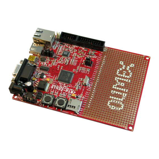
Page 3: Board Features
- Dimensions: 132.08x96.52mm (5.2x3.8") ELECTROSTATIC WARNING The STM32-P107 board is shipped in protective anti-static packaging. The board must not be subject to high electrostatic potentials. General practice for working with static sensitive devices should be applied when working with this board. -
Page 4: Board Use Requirements
ARM-USB-OCD-H you will need RS232 cable, too. Hardware: Programmer/Debugger – one of the Olimex ARM Programmers: ARM-JTAG, ARM- JTAG-EW, ARM-USB-OCD, ARM-USB-OCD-H, ARM-USB-OCD-TINY, ARM-USB-OCD-H. Note that Olimex OpenOCD debuggers lack SWD interface by default. There is the adapter ARM- JTAG-SWD that adds SWD to any of the programmers/debuggers mentioned above. - Page 5 – Debug mode – Serial wire debug (SWD) & JTAG interfaces – Cortex-M3 Embedded Trace Macrocell™ – 80 fast I/O ports – 80 I/Os, all mappable on 16 external interrupt vectors and almost all 5 V-tolerant – 10 timers – four 16-bit timers, each with up to 4 IC/OC/PWM or pulse counter and quadrature (incremental) encoder input –...
- Page 6 Page 6 of 19...
- Page 7 Page 7 of 19...
- Page 8 SCHEMATIC STM32-P107, board revision C 3 3V OLIMEX LTD, PLOVDIV, BULGARIA 2013 USB CIRCUIT VBUS https: /www.o imex com USB_HOST 3 3V_MCU_E HN1x3(O C ose H Open) C OSE USB_HOS KU USA S ADC 2_IN0 IM2_CH1_E R IM5_CH1 E H_M I_C S_WKU...
-
Page 9: Board Layout
– +5V_JTAG from JTAG The programmed board power consumption is about 70 mA. RESET CIRCUIT STM32-P107 reset circuit includes JTAG connector pin 15, U2 (STE101P) pin 28 (RESET), R73(10k), R74(330Ohm), R75(100Ohm/1%), C55(100nF), STM32F107 pin 14 (NRST) and RESET button. CLOCK CIRCUIT Quartz crystal 25 MHz is connected to STM32F107 pin 12 (OSC_IN) and pin 13 (OSC_OUT). -
Page 10: Jumper Description
JUMPER DESCRIPTION PWR_SEL When position 1-2 is shorted – the board is power supplied from JTAG. When position 3-4 is shorted – the board is power supplied from USB_OTG. When position 5-6 is shorted – the board is power supplied from External power source. - Page 11 3.3V_MCU_E Enable microcontroller 3.3V power supply Default state is closed. 3.3V_E Enable regulator VR2 (3.3V) - LM1117 Default state is closed. 3.3VA_E Enables board 3.3V analog power supply. Default state is closed. 3.3VA_MCU_E Enables microcontroller 3.3V analog power supply. Default state is closed. GNDA_E Enables board analog GND.
-
Page 12: Connector Descriptions
CONNECTOR DESCRIPTIONS JTAG The JTAG connector allows the software debugger to talk via a JTAG (Joint Test Action Group) port directly to the core. Instructions may be inserted and executed by the core thus allowing STM32F107 memory to be programmed with code and executed step by step by the host software. For more details please refer to IEEE Standard 1149.1 - 1990 Standard Test Access Port and Boundary Scan Architecture and STM32F107 datasheets and users manual. - Page 13 PWR_JACK Pin # Signal name Power input USB_HOST Pin # Signal name +5V_HOST_PWR USB_HOST_D- USB_HOST_D+ USB_OTG Pin # Signal name +5V_OTG_PWR USB_OTG_D- USB_OTG_D+ OTG_ID 3V_BAT Pin # Signal name VBAT...
- Page 14 RS232 The RS232 port can be used for communication when in bootloader mode. To enter bootloader mode you need to close RST_E and BOOT0_E jumpers. Note that the default position of those jumpers is closed, e.g. bootloader mode disabled. Pin # Signal name T1OUT R1IN...
- Page 15 Pin # Signal name chip side Pin # Signal name chip side Not connected (NC) Not connected (NC) Color Usage Right Green Link status Left Yellow Activity status SD/MMC Pin # Signal name MCIDAT2 CS_MMC SPI3_MOSI 3.3V SPI3_SCK SPI3_MISO MCIDAT1 Not connected Not connected Not connected...
-
Page 16: Mechanical Dimensions
AVAILABLE DEMO SOFTWARE All demo examples are available at the board's web-page (https://www.olimex.com/Products/ARM/ST/STM32-P107/) and wiki article (https://www.olimex.com/wiki/STM32-P107). Make sure that the demo you download is compatible with the board revision you have! The board revision is printed on STM32-P107 itself. -
Page 17: Revision And Ordering Information
REVISION AND ORDERING INFORMATION STM32-P107 – fully assembled and tested Manual revision history: REV. I - created December 2009 REV. A - edited by TU December 2010 REV. B - demo software added and mechanical dimensions detaile REV. C - rev. A schematic and added more programmers in BOARD USE REQUIREMENTS. - Page 18 rev. C ======== 1. L2 is now placed further from USB_HOST connector to avoid contact 2. Ethernet PHY Micrel KS8721 is changed to LAN8710A-EZC in RMII 3. Changed C18 from 100n to 4.7uF/6.3V according to the datasheet. C18 is now renamed C3. 4.
Need help?
Do you have a question about the STM32-P107 and is the answer not in the manual?
Questions and answers