
Related Manuals for OLIMEX STM32-P107


Summary of Contents for OLIMEX STM32-P107
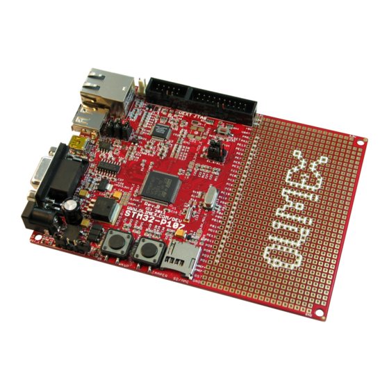
- Page 1 STM32-P107 development board User's manual All boards produced by Olimex are ROHS compliant Document revision L, Feburary 2018 Copyright(c) 2014, OLIMEX Ltd, All rights reserved Page 1 of 23...
- Page 2 This document is intended only to assist the reader in the use of the product. OLIMEX Ltd. shall not be liable for any loss or damage arising from the use of any information in this document or any error or omission in such information or any incorrect use of the product.
-
Page 3: Board Features
- Dimensions: (5.2×3.8)'' ~ (132×97)mm ELECTROSTATIC WARNING The STM32-P107 board is shipped in protective anti-static packaging. The board must not be subject to high electrostatic potentials. General practice for working with static sensitive devices should be applied when working with this board. -
Page 4: Board Use Requirements
ARM-USB-OCD-H you will need RS232 cable, too. Hardware: Programmer/Debugger – one of the Olimex ARM Programmers: ARM-JTAG, ARM- JTAG-EW, ARM-USB-OCD, ARM-USB-OCD-H, ARM-USB-OCD-TINY, ARM-USB-OCD-H. Note that Olimex OpenOCD debuggers lack SWD interface by default. There is the adapter ARM- JTAG-SWD that adds SWD to any of the programmers/debuggers mentioned above. -
Page 5: Processor Features
PROCESSOR FEATURES STM32-P107 board uses the ARM-based 32-bit microcontroller STM32F107VCT6 with the following features: – Core: ARM 32-bit Cortex™-M3 CPU – 72 MHz maximum frequency, 1.25 DMIPS/MHz (Dhrystone 2.1) performance at 0 wait state memory access – Single-cycle multiplication and hardware division –... -
Page 6: Stm32F107 Block Diagram
STM32F107 BLOCK DIAGRAM Page 6 of 23... -
Page 7: Stm32F107 Memory Map
STM32F107 MEMORY MAP Page 7 of 23... - Page 8 SCHEMATIC 3.3V STM32-P107, board revision C VBUS USB CIRCUIT USB_HOST 3.3V_MCU_E HN1x3(O:Close,H:Open) CLOSE USB_HOST OTG_VBUS +5V_HOST_PWR PA0/WKUP/USART2_CTS/ADC12_IN0/TIM2_CH1_ETR/TIM5_CH1/ETH_MII_CRS_WKUP WKUP PA1/USART2_RTS/ADC12_IN1/TIM5_CH2/TIM2_CH2/ETH_MII_RX_CLK/ETH_RMII_REF_CLK +5V_OTG_PWR +5V_HOST_PWR ETH_RMII_REF_CLK ETH_RMII_REF_CLK +5V_HOST_PWR 0R(Board_Mounted) PA2/USART2_TX/TIM5_CH3/ADC12_IN2/TIM2_CH3/ETH_MII_MDIO/ETH_RMII_MDIO ETH_RMII_MDIO ETH_RMII_MDIO USB_HOST_D- USB_HOST_D- USB_HOST_D+ PA3/USART2_RX/TIM5_CH4/ADC12_IN3/TIM2_CH4/ETH_MII_COL USB_HOST_D+ PA4/SPI1_NSS/DAC_OUT1/USART2_CK/ADC12_IN4 CS_MMC CS_MMC PA5/SPI1_SCK/DAC_OUT2/ADC12_IN5 SHIELD PA6/SPI1_MISO/ADC12_IN6/TIM3_CH1/TIM1_BKIN PA7/SPI1_MOSI/ADC12_IN7/TIM3_CH2/ETH_MII_RX_DV/ETH_RMII_CRS_DV/TIM1_CH1N...
-
Page 9: Board Layout
The programmed board power consumption is about 70 mA. RESET CIRCUIT STM32-P107 reset circuit includes JTAG connector pin 15, U2 (STE101P) pin 28 (RESET), R73 (10k), R74 (330Ohm), R75 (100Ohm/1%), C55 (100nF), STM32F107 pin 14 (NRST) and RESET button. CLOCK CIRCUIT Quartz crystal 25 MHz is connected to STM32F107 pin 12 (OSC_IN) and pin 13 (OSC_OUT). -
Page 10: Jumper Description
JUMPER DESCRIPTION STM32-P107 has a number of jumpers. They control the behavior of the board and allow modification of the default hardware connections. There are two types of jumpers – PTH ones (big ones, easy to change using a plastic cap) and SMT ones (pads that require cutting and soldering). It is safe to change the position of the PTH jumpers as long as you use one of the legal positions of the jumper. - Page 11 SMT jumpers: The SMT jumpers are typically used for hardware measurements and hardware debugging. Please do not attempt to change the jumpers if you lack the soldering skills required. 3.3V_MCU_E Enable microcontroller 3.3V power supply Default state is closed. 3.3V_E Enable regulator VR2 (3.3V) - LM1117 Default state is closed.
-
Page 12: Connector Descriptions
CONNECTOR DESCRIPTIONS JTAG The JTAG connector is used to program and debug the board via a third-party tool. It can be used for JTAG and SWD programming and debugging. It is recommended to use with tools that have a compatible 20-pin 0.1 step connector. -
Page 13: Power Input
PWR_JACK The board has a standard Olimex DC barrel jack with 2.0mm inner pin and 6.3mm hole. More information about the exact component might be found here: https://www.olimex.com/wiki/PWRJACK You can supply either DC or AC voltage to power the board however be careful – if you provide more than the maximum voltage suggested, you would permanently damage the board. - Page 14 To enter the DFU mode you would also need to set the STM32-P107's jumpers properly. Make sure all jumpers are set as per default and then change the jumper B0_0/B0_1 to position B0_1 – which means boot from system memory.
- Page 15 RS232 The board can be programmed via the RS232 connector (serial interface). This is done without the need of an additional programming tool. However, you would need a proper serial cable or adapter to access it. You would also need to change the positions of three PTH jumpers (the rest of the jumpers should be as per default): 1.
- Page 16 Pin # Signal name T1OUT R1IN UEXT The UEXT connector is typically used to attach additional modules to the board. It nests three popular interfaces – UART, I2C, and SPI. You can also find 3.3V power output and GND (respectively, pin #1 and pin #2).
- Page 17 Pin # Signal name chip side Pin # Signal name chip side Not connected (NC) Not connected (NC) Color Usage Right Green Link status Left Yellow Activity status 3V_BAT Pin # Signal name VBAT Page 17 of 23...
-
Page 18: Mechanical Dimensions
MECHANICAL DIMENSIONS All measures are in mils. Page 18 of 23... - Page 19 Proto area pad pinout table: WHITE PRINT ROW #1 PORT PROCESSOR WHITE PRINT ROW #2 PORT PROCESSOR 3.3V 3.3V 3.3VA AGND VBAT PE14 PE13 PE12 PE11 PE13 PE12 PE10 PE11 PE10 PC11 PC12 PC10 PC13 PC11 PC14 PB10 PB11 PB15 PB10 PB14 PD14...
-
Page 20: Available Demo Software
All demo examples are available at the board's web-page (https://www.olimex.com/Products/ARM/ST/STM32-P107/) and wiki article (https://www.olimex.com/wiki/STM32-P107). Make sure that the demo you download is compatible with the board revision you have! The board revision is printed on STM32-P107 itself. Page 20 of 23... -
Page 21: Revisions And Ordering Information
STM32-P107 – fully assembled and tested You can purchase directly from our online shop or from any of our distributors. Note that usually it is faster and cheaper to purchase Olimex products from our distributors. List of confirmed Olimex LTD distributors and resellers: https://www.olimex.com/Distributors. - Page 22 6. A lot of jumpers are added into the jumpers description table rev. C ======== 1. L2 is now placed further from USB_HOST connector to avoid contact 2. Ethernet PHY Micrel KS8721 is changed to LAN8710A-EZC in RMII 3. Changed C18 from 100n to 4.7uF/6.3V according to the datasheet. C18 is now renamed C3. 4.
-
Page 23: Warranty And Support
All goods are checked before they are sent out. In the unlikely event that goods are faulty, they must be returned, to OLIMEX at the address listed on your order invoice. OLIMEX will not accept goods that have clearly been used more than the amount needed to evaluate their functionality. - Page 24 Mouser Electronics Authorized Distributor Click to View Pricing, Inventory, Delivery & Lifecycle Information: Olimex Ltd. STM32-P107...
Need help?
Do you have a question about the STM32-P107 and is the answer not in the manual?
Questions and answers