Table of Contents
Advertisement
Quick Links
This user's guide describes the characteristics, operation, and use of the INA253EVM evaluation module.
The user's guide discusses how to set up and configure the hardware and reviews various aspects of the
hardware operation. Throughout this document, the terms evaluation board, evaluation module, and EVM
are synonymous with the INA253EVM. This document also includes an electrical schematic, printed circuit
board (PCB) layout drawings, and a parts list for the EVM.
SBOU194 – May 2018
Submit Documentation Feedback
Copyright © 2018, Texas Instruments Incorporated
User's Guide
SBOU194 – May 2018
INA253EVM
1
INA253EVM
Advertisement
Table of Contents

Related Manuals for Texas Instruments INA253EVM


Summary of Contents for Texas Instruments INA253EVM
- Page 1 SBOU194 – May 2018 INA253EVM This user’s guide describes the characteristics, operation, and use of the INA253EVM evaluation module. The user's guide discusses how to set up and configure the hardware and reviews various aspects of the hardware operation. Throughout this document, the terms evaluation board, evaluation module, and EVM are synonymous with the INA253EVM.
-
Page 2: Table Of Contents
PCB Bottom Layer List of Tables ....................INA253EVM Kit Contents ..................... Related Documentation ....................... Bill of Materials Trademarks All trademarks are the property of their respective owners. INA253EVM SBOU194 – May 2018 Submit Documentation Feedback Copyright © 2018, Texas Instruments Incorporated... -
Page 3: Overview
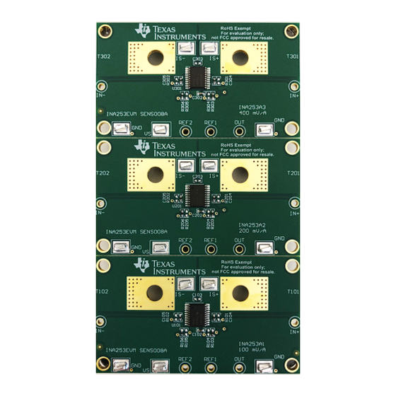
INA253A1, INA253A2, and INA253A3 (all referred to as INA253Ax). The INA253EVM consists of one PCB with an option to cut out three individual PCBs. Each of the PCB cutouts consists of the INA253Ax device (where Ax is A1, A2, and A3, for boards 1 through 3, respectively), and test points for external hardware connections. -
Page 4: Hardware
Hardware Each of the PCBs on the INA253EVM requires a 2.7-V to 5.5-V power supply connected between the VS and GND test points. The INA253 family of devices have an integrated shunt of value 2 mΩ between the IS+ and IS– pins. -
Page 5: Features
Hardware www.ti.com Features The INA253EVM provides basic functional evaluation of this device family. The fixture layout is not intended for electromagnetic compatibility (EMC) testing. The INA253EVM PCB provides the following features: • All INA253 devices are provided • Easy access to all pins •... -
Page 6: Schematic, Pcb Layout, And Bill Of Materials
GND1 R101 R102 GND1 GND1 R103 REF1 REF2 R104 TP107 R105 R106 INA253A1IPWR TP106 TP103 GND1 GND1 TP110 TP109 GND1 Figure 2. INA253Ax Test Board Schematic INA253EVM SBOU194 – May 2018 Submit Documentation Feedback Copyright © 2018, Texas Instruments Incorporated... -
Page 7: Pcb Layout
IS– pins. Use a 2-oz copper pour to improve the heat-dissipation capabilities, and thus increase the continuous-load current capacity. Using the INA253EVM board with this robust layout and airflow, the INA253 device safely accommodates up to 15 A of current over the entire –40°C to +85°C temperature range. -
Page 8: Pcb Top Layer
Schematic, PCB Layout, and Bill of Materials www.ti.com Figure 4. PCB Top Layer Figure 5. PCB Bottom Layer INA253EVM SBOU194 – May 2018 Submit Documentation Feedback Copyright © 2018, Texas Instruments Incorporated... -
Page 9: Bill Of Materials
Schematic, PCB Layout, and Bill of Materials www.ti.com Bill of Materials Table 3 lists the bill of materials (BOM) for the INA253EVM. Table 3. Bill of Materials Quantity Designator Description PartNumber Manufacturer CAP, CERM, 0.1 µF, 16 V, +/- 10%,... - Page 10 STANDARD TERMS FOR EVALUATION MODULES Delivery: TI delivers TI evaluation boards, kits, or modules, including any accompanying demonstration software, components, and/or documentation which may be provided together or separately (collectively, an “EVM” or “EVMs”) to the User (“User”) in accordance with the terms set forth herein.
- Page 11 FCC Interference Statement for Class B EVM devices NOTE: This equipment has been tested and found to comply with the limits for a Class B digital device, pursuant to part 15 of the FCC Rules. These limits are designed to provide reasonable protection against harmful interference in a residential installation.
- Page 12 【無線電波を送信する製品の開発キットをお使いになる際の注意事項】 開発キットの中には技術基準適合証明を受けて いないものがあります。 技術適合証明を受けていないもののご使用に際しては、電波法遵守のため、以下のいずれかの 措置を取っていただく必要がありますのでご注意ください。 1. 電波法施行規則第6条第1項第1号に基づく平成18年3月28日総務省告示第173号で定められた電波暗室等の試験設備でご使用 いただく。 2. 実験局の免許を取得後ご使用いただく。 3. 技術基準適合証明を取得後ご使用いただく。 なお、本製品は、上記の「ご使用にあたっての注意」を譲渡先、移転先に通知しない限り、譲渡、移転できないものとします。 上記を遵守頂けない場合は、電波法の罰則が適用される可能性があることをご留意ください。 日本テキサス・イ ンスツルメンツ株式会社 東京都新宿区西新宿6丁目24番1号 西新宿三井ビル 3.3.3 Notice for EVMs for Power Line Communication: Please see http://www.tij.co.jp/lsds/ti_ja/general/eStore/notice_02.page 電力線搬送波通信についての開発キットをお使いになる際の注意事項については、次のところをご覧ください。http:/ /www.tij.co.jp/lsds/ti_ja/general/eStore/notice_02.page 3.4 European Union 3.4.1 For EVMs subject to EU Directive 2014/30/EU (Electromagnetic Compatibility Directive): This is a class A product intended for use in environments other than domestic environments that are connected to a low-voltage power-supply network that supplies buildings used for domestic purposes.
- Page 13 Notwithstanding the foregoing, any judgment may be enforced in any United States or foreign court, and TI may seek injunctive relief in any United States or foreign court. Mailing Address: Texas Instruments, Post Office Box 655303, Dallas, Texas 75265 Copyright © 2018, Texas Instruments Incorporated...
- Page 14 IMPORTANT NOTICE FOR TI DESIGN INFORMATION AND RESOURCES Texas Instruments Incorporated (‘TI”) technical, application or other design advice, services or information, including, but not limited to, reference designs and materials relating to evaluation modules, (collectively, “TI Resources”) are intended to assist designers who are developing applications that incorporate TI products;...
- Page 15 Mouser Electronics Authorized Distributor Click to View Pricing, Inventory, Delivery & Lifecycle Information: Texas Instruments INA253EVM...
Need help?
Do you have a question about the INA253EVM and is the answer not in the manual?
Questions and answers