Table of Contents
Advertisement
Quick Links
Features
®
•
Utilizes the AVR
RISC Architecture
•
AVR – High-performance and Low-power RISC Architecture
– 118 Powerful Instructions – Most Single Clock Cycle Execution
– 32 x 8 General Purpose Working Registers
– Up to 10 MIPS Throughput at 10 MHz
•
Data and Non-volatile Program Memory
– 2K Bytes of In-System Programmable Flash
Endurance 1,000 Write/Erase Cycles
– 128 Bytes of SRAM
– 128 Bytes of In-System Programmable EEPROM
Endurance: 100,000 Write/Erase Cycles
– Programming Lock for Flash Program and EEPROM Data Security
•
Peripheral Features
– One 8-bit Timer/Counter with Separate Prescaler
– One 16-bit Timer/Counter with Separate Prescaler,
Compare, Capture Modes and 8-, 9-, or 10-bit PWM
– On-chip Analog Comparator
– Programmable Watchdog Timer with On-chip Oscillator
– SPI Serial Interface for In-System Programming
– Full Duplex UART
•
• Special Microcontroller Features
– Low-power Idle and Power-down Modes
– External and Internal Interrupt Sources
•
• Specifications
– Low-power, High-speed CMOS Process Technology
– Fully Static Operation
•
Power Consumption at 4 MHz, 3V, 25°C
– Active: 2.8 mA
– Idle Mode: 0.8 mA
– Power-down Mode: <1 µA
•
I/O and Packages
– 15 Programmable I/O Lines
– 20-pin PDIP and SOIC
•
Operating Voltages
– 2.7 - 6.0V (AT90S2313-4)
– 4.0 - 6.0V (AT90S2313-10)
•
Speed Grades
– 0 - 4 MHz (AT90S2313-4)
– 0 - 10 MHz (AT90S2313-10)
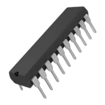
Pin Configuration
PDIP/SOIC
8-bit
Microcontroller
with 2K Bytes
of In-System
Programmable
Flash
AT90S2313
Rev. 0839I–AVR–06/02
1
Advertisement
Table of Contents

Related Manuals for Atmel AT90S4433-8AC


Summary of Contents for Atmel AT90S4433-8AC
-
Page 1: Table Of Contents Features
Features ® • Utilizes the AVR RISC Architecture • AVR – High-performance and Low-power RISC Architecture – 118 Powerful Instructions – Most Single Clock Cycle Execution – 32 x 8 General Purpose Working Registers – Up to 10 MIPS Throughput at 10 MHz •... -
Page 2: Description
Description The AT90S2313 is a low-power CMOS 8-bit microcontroller based on the AVR RISC architecture. By executing powerful instructions in a single clock cycle, the AT90S2313 achieves throughputs approaching 1 MIPS per MHz allowing the system designer to optimize power consumption versus processing speed. The AVR core combines a rich instruction set with 32 general purpose working registers. -
Page 3: Pin Descriptions
Power-down mode saves the register contents but freezes the Oscillator, disabling all other chip functions until the next external interrupt or Hardware Reset. The device is manufactured using Atmel’s high-density non-volatile memory technology. The On-chip In-System Programmable Flash allows the Program memory to be repro- grammed in-system through an SPI serial interface or by a conventional non-volatile memory programmer. -
Page 4: Crystal Oscillator
Crystal Oscillator XTAL1 and XTAL2 are input and output, respectively, of an inverting amplifier that can be configured for use as an On-chip Oscillator, as shown in Figure 2. Either a quartz crystal or a ceramic resonator may be used. To drive the device from an external clock source, XTAL2 should be left unconnected while XTAL1 is driven, as shown in Figure 3. -
Page 5: Architectural Overview
AT90S2313 Architectural The fast-access Register File concept contains 32 x 8-bit general purpose working reg- isters with a single clock cycle access time. This means that during one single clock Overview cycle, one ALU (Arithmetic Logic Unit) operation is executed. Two operands are output from the Register File, the operation is executed, and the result is stored back in the Register File –... - Page 6 The I/O memory space contains 64 addresses for CPU peripheral functions such as control registers, Timer/Counters, A/D converters and other I/O functions. The I/O mem- ory can be accessed directly or as the Data Space locations following those of the Register File, $20 - $5F.
-
Page 7: General Purpose Register File
AT90S2313 General Purpose Figure 6 shows the structure of the 32 general purpose registers in the CPU. Register File Figure 6. AVR CPU General Purpose Working Registers Addr. … General Purpose Working Registers … X-register Low Byte X-register High Byte Y-register Low Byte Y-register High Byte Z-register Low Byte... -
Page 8: Alu - Arithmetic Logic Unit
In the different addressing modes these address registers have functions as fixed dis- placement, automatic increment and decrement (see the descriptions for the different instructions). ALU – Arithmetic Logic The high-performance AVR ALU operates in direct connection with all the 32 general Unit purpose working registers. -
Page 9: Sram Data Memory
AT90S2313 SRAM Data Memory Figure 8 shows how the AT90S2313 data memory is organized. Figure 8. SRAM Organization Register File Data Address Space … … I/O Registers … … Internal SRAM … The 224 data memory locations address the Register File, I/O memory and the data SRAM. -
Page 10: Program And Data Addressing Modes
Program and Data The AT90S2313 AVR RISC microcontroller supports powerful and efficient addressing modes for access to the Program memory (Flash) and Data memory. This section Addressing Modes describes the different addressing modes supported by the AVR architecture. In the fig- ures, OP means the operation code part of the instruction word. - Page 11 AT90S2313 Operand address is contained in 6 bits of the instruction word. n is the destination or source register address. Data Direct Figure 12. Direct Data Addressing A 16-bit data address is contained in the 16 LSBs of a 2-word instruction. Rd/Rr specify the destination or source register.
- Page 12 Data Indirect with Pre- Figure 15. Data Indirect Addressing with Pre-decrement decrement The X-, Y-, or Z-register is decremented before the operation. Operand address is the decremented contents of the X-, Y-, or Z-register. Data Indirect with Post- Figure 16. Data Indirect Addressing with Post-increment increment The X-, Y-, or Z-register is incremented after the operation.
- Page 13 AT90S2313 Indirect Program Addressing, Figure 18. Indirect Program Memory Addressing IJMP and ICALL Program execution continues at address contained by the Z-register (i.e., the PC is loaded with the contents of the Z-register). Relative Program Addressing, Figure 19. Relative Program Memory Addressing RJMP and RCALL Program execution continues at address PC + k + 1.
-
Page 14: Memory Access And Instruction Execution Timing
Memory Access and This section describes the general access timing concepts for instruction execution and internal memory access. Instruction Execution Timing The AVR CPU is driven by the System Clock Ø, directly generated from the external clock crystal for the chip. No internal clock division is used. Figure 20 shows the parallel instruction fetches and instruction executions enabled by the Harvard architecture and the fast-access Register File concept. -
Page 15: I/O Memory
AT90S2313 Figure 22. On-chip Data SRAM Access Cycles System Clock Ø Address Prev. Address Address Data Data I/O Memory The I/O space definition of the AT90S2313 is shown in Table 1. Table 1. AT90S2313 I/O Space Address Hex Name Function $3F ($5F) SREG Status Register... - Page 16 Table 1. AT90S2313 I/O Space (Continued) Address Hex Name Function $12 ($32) PORTD Data Register, Port D $11 ($31) DDRD Data Direction Register, Port D $10 ($30) PIND Input Pins, Port D $0C ($2C) UART I/O Data Register $0B ($2B) UART Status Register $0A ($2A) UART Control Register...
- Page 17 AT90S2313 • Bit 5 – H: Half-carry Flag The Half-carry Flag H indicates a Half-carry in some arithmetic operations. See the Instruction Set description for detailed information. • Bit 4 – S: Sign Bit, S = N ⊕ V The S-bit is always an exclusive or between the Negative Flag N and the Two’s Comple- ment Overflow Flag V.
-
Page 18: Reset And Interrupt Handling
Reset and Interrupt The AT90S2313 provides 10 different interrupt sources. These interrupts and the sepa- rate Reset Vector each have a separate Program Vector in the program memory space. Handling All the interrupts are assigned individual enable bits that must be set (one) together with the I-bit in the Status Register in order to enable the interrupt. - Page 19 AT90S2313 Reset Sources The AT90S2313 has three sources of reset: • Power-on Reset. The MCU is reset when the supply voltage is below the Power-on Reset threshold (V • External Reset. The MCU is reset when a low level is present on the RESET pin for more than 50 ns.
- Page 20 Table 4. Number of Watchdog Oscillator Cycles FSTRT Time-out at V = 5V Number of WDT Cycles Programmed 0.28 ms Unprogrammed 16.0 ms Power-on Reset A Power-on Reset (POR) circuit ensures that the device is reset from Power-on. As shown in Figure 23, an internal timer is clocked from the Watchdog Timer. This timer prevents the MCU from starting until after a certain period after V has reached the Power-on Threshold voltage (V...
- Page 21 AT90S2313 External Reset An External Reset is generated by a low level on the RESET pin. Reset pulses longer than 50 ns will generate a reset, even if the clock is not running. Shorter pulses are not guaranteed to generate a reset. When the applied signal reaches the Reset Threshold Voltage (V ) on its positive edge, the delay timer starts the MCU after the Time-out period t...
- Page 22 interrupt. Some of the Interrupt Flags can also be cleared by writing a logical “1” to the flag bit position(s) to be cleared. If an interrupt condition occurs when the corresponding interrupt enable bit is cleared (zero), the Interrupt Flag will be set and remembered until the interrupt is enabled, or the flag is cleared by software.
- Page 23 AT90S2313 General Interrupt FLAG Register – GIFR $3A ($5A) INTF1 INTF0 – – – – – – GIFR Read/Write Initial value • Bit 7 – INTF1: External Interrupt Flag1 When an edge on the INT1 pin triggers an interrupt request, the corresponding Interrupt Flag, INTF1, becomes set (one).
- Page 24 • Bit 3 – TICIE1: Timer/Counter1 Input Capture Interrupt Enable When the TICIE1 bit is set (one) and the I-bit in the Status Register is set (one), the Timer/Counter1 Input Capture Event Interrupt is enabled. The corresponding interrupt (at vector $003) is executed if a capture-triggering event occurs on PD6(ICP) (i.e., when the ICF1 bit is set in the Timer/Counter Interrupt Flag Register [TIFR]).
- Page 25 AT90S2313 • Bit 2 – Res: Reserved Bit This bit is a reserved bit in the AT90S2313 and always reads as zero. • Bit 1 – TOV0: Timer/Counter0 Overflow Flag The bit TOV0 is set (one) when an overflow occurs in Timer/Counter0. TOV0 is cleared by hardware when executing the corresponding interrupt handling vector.
- Page 26 • Bit 4 – SM: Sleep Mode This bit selects between the two available sleep modes. When SM is cleared (zero), Idle mode is selected as sleep mode. When SM is set (one), Power-down mode is selected as sleep mode. For details, refer to the paragraph “Sleep Modes”. •...
-
Page 27: Sleep Modes
AT90S2313 Sleep Modes To enter the sleep modes, the SE bit in MCUCR must be set (one) and a SLEEP instruc- tion must be executed. If an enabled interrupt occurs while the MCU is in a sleep mode, the MCU awakes, executes the interrupt routine, and resumes execution from the instruction following SLEEP. -
Page 28: 8-Bit Timer/Counter0
The four different prescaled selections are: CK/8, CK/64, CK/256, and CK/1024, where CK is the Oscillator clock. For the two Timer/Counters, added selections such as CK, external clock source and stop can be selected as clock sources. 8-bit Timer/Counter0 Figure 29 shows the block diagram for Timer/Counter0. The 8-bit Timer/Counter0 can select clock source from CK, prescaled CK or an external p in . - Page 29 AT90S2313 Timer/Counter0 Control Register – TCCR0 $33 ($53) – – – – – CS02 CS01 CS00 TCCR0 Read/Write Initial value • Bits 7..3 – Res: Reserved Bits These bits are reserved bits in the AT90S2313 and always read zero. • Bits 2,1,0 – CS02, CS01, CS00: Clock Select0, Bit 2,1 and 0 The Clock Select0 bits 2, 1, and 0 define the prescaling source of Timer/Counter0.
-
Page 30: 16-Bit Timer/Counter1
16-bit Timer/Counter1 Figure 30 shows the block diagram for Timer/Counter1. Figure 30. Timer/Counter1 Block Diagram The 16-bit Timer/Counter1 can select clock source from CK, prescaled CK or an exter- nal pin. In addition, it can be stopped as described in the specification for the Timer/Counter1 Control Register (TCCR1B). - Page 31 AT90S2313 Timer/Counter1 can also be used as an 8-, 9-, or 10-bit Pulse Width Modulator. In this mode the counter and the OCR1 Register serve as a glitch-free standalone PWM with centered pulses. Refer to page 35 for a detailed description of this function. The Input Capture function of Timer/Counter1 provides a capture of the Timer/Counter1 contents to the Input Capture Register (ICR1), triggered by an external event on the Input Capture Pin (ICP).
- Page 32 • Bits 1, 0 – PWM11, PWM10: Pulse Width Modulator Select Bits These bits select PWM operation of Timer/Counter1 as specified in Table 9. This mode is described on page 35. Table 9. PWM Mode Select PWM11 PWM10 Description PWM operation of Timer/Counter1 is disabled Timer/Counter1 is an 8-bit PWM Timer/Counter1 is a 9-bit PWM Timer/Counter1 is a 10-bit PWM...
- Page 33 AT90S2313 • Bits 2,1,0 – CS12, CS11, CS10: Clock Select1, Bits 2, 1 and 0 The Clock Select1 bits 2, 1, and 0 define the prescaling source of Timer/Counter1. Table 10. Clock 1 Prescale Select CS12 CS11 CS10 Description Stop, the Timer/Counter1 is stopped. CK/8 CK/64 CK/256...
- Page 34 The Timer/Counter1 is realized as an up or up/down (in PWM mode) counter with read and write access. If Timer/Counter1 is written to and a clock source is selected, the Timer/Counter1 continues counting in the timer clock cycle after it is preset with the writ- ten value.
- Page 35 AT90S2313 The TEMP Register is also used when accessing TCNT1 and OCR1A. If the main pro- gram and interrupt routines perform access to registers using TEMP, interrupts must be disabled during access from the main program or interrupts if interrupts are re-enabled. Timer/Counter1 in PWM Mode When the PWM mode is selected, Timer/Counter1 and the Output Compare Register1 (OCR1A) form an 8-, 9-, or 10-bit, free-running, glitch-free and phase-correct PWM with...
- Page 36 During the time between the write and the latch operations, a read from OCR1A will read the contents of the temporary location. This means that the most recently written value always will read out of OCR1A. When the OCR1 contains $0000 or TOP, the output OC1 is updated to low or high on the next compare match according to the settings of COM1A1/COM1A0.
-
Page 37: Watchdog Timer
AT90S2313 Watchdog Timer The Watchdog Timer is clocked from a separate On-chip Oscillator that runs at 1 MHz. This is the typical value at V = 5V. See characterization data for typical values at other levels. By controlling the Watchdog Timer prescaler, the Watchdog Reset interval can be adjusted. - Page 38 1. In the same operation, write a logical “1” to WDTOE and WDE. A logical “1” must be written to WDE even though it is set to 1 before the disable operation starts. 2. Within the next four clock cycles, write a logical “0” to WDE. This disables the Watchdog.
-
Page 39: Eeprom Read/Write Access
AT90S2313 EEPROM Read/Write The EEPROM Access Registers are accessible in the I/O space. Access The write access time is in the range of 2.5 - 4 ms, depending on the V voltages. A self-timing function, however, lets the user software detect when the next byte can be written. - Page 40 EEPROM Control Register – EECR $1C ($3C) – – – – – EEMWE EEWE EERE EECR Read/Write Initial value • Bit 7..3 – Res: Reserved Bits These bits are reserved bits in the AT90S2313 and will always read as zero. •...
-
Page 41: Prevent Eeprom Corruption
AT90S2313 Prevent EEPROM During periods of low V , the EEPROM data can be corrupted because the supply volt- age is too low for the CPU and the EEPROM to operate properly. These issues are the Corruption same as for board-level systems using the EEPROM, and the same design solutions should be applied. -
Page 42: Uart
UART The AT90S2313 features a full duplex (separate Receive and Transmit Registers) Uni- versal Asynchronous Receiver and Transmitter (UART). The main features are: • Baud Rate Generator that can Generate a Large Number of Baud Rates (bps) • High Baud Rates at Low XTAL Frequencies •... -
Page 43: Data Reception
AT90S2313 tus Register (USR) is set. When this bit is set (one), the UART is ready to receive the next character. At the same time as the data is transferred from UDR to the 10(11)-bit Shift Register, bit 0 of the Shift Register is cleared (start bit) and bit 9 or 10 is set (stop bit). - Page 44 found to be logical “1”s, the start bit is rejected as a noise spike and the receiver starts looking for the next 1-to-0 transition. If, however, a valid start bit is detected, sampling of the data bits following the start bit is performed.
-
Page 45: Uart Control
AT90S2313 UART Control The UART I/O Data Register – $0C ($2C) Read/Write Initial value The UDR Register is actually two physically separate registers sharing the same I/O address. When writing to the register, the UART Transmit Data Register is written. When reading from UDR, the UART Receive Data Register is read. - Page 46 • Bit 4 – FE: Framing Error This bit is set if a Framing Error condition is detected (i.e., when the stop bit of an incom- ing character is zero). The FE bit is cleared when the stop bit of received data is one. •...
- Page 47 AT90S2313 • Bit 1 – RXB8: Receive Data Bit 8 When CHR9 is set (one), RXB8 is the ninth data bit of the received character. • Bit 0 – TXB8: Transmit Data Bit 8 When CHR9 is set (one), TXB8 is the ninth data bit in the character to be transmitted. Baud Rate Generator The baud rate generator is a frequency divider that generates baud rates according to the following equation:...
-
Page 48: Analog Comparator
UART Baud Rate Register – UBRR $09 ($29) UBRR Read/Write Initial value The UBRR Register is an 8-bit read/write register that specifies the UART Baud Rate according to the formula on the previous page. Analog Comparator The Analog Comparator compares the input values on the positive input AIN0 (PB0) and the negative input PB1(AIN1). - Page 49 AT90S2313 • Bit 5 – ACO: Analog Comparator Output ACO is directly connected to the comparator output. • Bit 4 – ACI: Analog Comparator Interrupt Flag This bit is set (one) when a comparator output event triggers the interrupt mode defined by ACIS1 and ACIS0.
-
Page 50: I/O Ports
I/O Ports All AVR ports have true Read-Modify-Write functionality when used as general digital I/O ports. This means that the direction of one port pin can be changed without uninten- tionally changing the direction of any other pin with the SBI and CBI instructions. The same applies for changing drive value (if configured as output) or enabling/disabling of pull-up resistors (if configured as input). - Page 51 AT90S2313 The Port B Input Pins address (PINB) is not a register; this address enables access to the physical value on each Port B pin. When reading PORTB, the Port B Data Latch is read, and when reading PINB, the logical values present on the pins are read. Port B as General Digital I/O All eight pins in Port B have equal functionality when used as digital I/O pins.
- Page 52 Port B Schematics Note that all port pins are synchronized. The synchronization latches are, however, not shown in the figures. Figure 38. Port B Schematic Diagram (Pins PB0 and PB1) AT90S2313 0839I–AVR–06/02...
- Page 53 AT90S2313 Figure 39. Port B Schematic Diagram (Pin PB3) PULL- RESET DDB3 RESET PORTB3 COM1A0 WRITE PORTB COM1A1 WRITE DDRB READ PORTB LATCH OUTPUT READ PORTB PIN COMP. MATCH1 MODE SELECT READ DDRB Figure 40. Port B Schematic Diagram (Pins PB2 and PB4) 0839I–AVR–06/02...
- Page 54 Figure 41. Port B Schematic Diagram (Pin PB5) Figure 42. Port B Schematic Diagram (Pin PB6) AT90S2313 0839I–AVR–06/02...
-
Page 55: Port D
AT90S2313 Figure 43. Port B Schematic Diagram (Pin PB7) Port D Three I/O memory address locations are allocated for the Port D: one each for the Data Register – PORTD, $12($32), Data Direction Register – DDRD, $11($31) and the Port D Input Pins –... - Page 56 Port D Data Register – PORTD $12 ($32) – PORTD6 PORTD5 PORTD4 PORTD3 PORTD2 PORTD1 PORTD0 PORTD Read/Write Initial value Port D Data Direction Register – DDRD $11 ($31) – DDD6 DDD5 DDD4 DDD3 DDD2 DDD1 DDD0 DDRD Read/Write Initial value Port D Input Pins Address –...
- Page 57 AT90S2313 • INT1 – Port D, Bit 3 INT1, External Interrupt Source 1. The PD3 pin can serve as an external interrupt source to the MCU. See the interrupt description for further details and how to enable the source. • INT0 – Port D, Bit 2 INT0, External Interrupt Source 0.
- Page 58 Figure 45. Port D Schematic Diagram (Pin PD1) PULL- RESET DDD1 RESET PORTD1 WRITE PORTD TXEN WRITE DDRD READ PORTD LATCH READ PORTD PIN READ DDRD TXD: UART TRANSMIT DATA UART TRANSMIT ENABLE TXEN: Figure 46. Port D Schematic Diagram (Pins PD2 and PD3) AT90S2313 0839I–AVR–06/02...
- Page 59 AT90S2313 Figure 47. Port D Schematic Diagram (Pins PD4 and PD5) PULL- RESET DDDn RESET PORTDn WRITE PORTD TIMERm CLOCK WRITE DDRD SENSE CONTROL SOURCE MUX READ PORTD LATCH READ PORTD PIN READ DDRD 4, 5 0, 1 CSm0 CSm2 CSm1 Figure 48.
-
Page 60: Memory Programming
Chip Erase. Signature Bytes All Atmel microcontrollers have a 3-byte signature code that identifies the device. This code can be read in both serial and parallel mode. The three bytes reside in a separate address space. -
Page 61: Parallel Programming
AT90S2313 within the self-timed write instruction in the Serial Programming mode. During program- ming, the supply voltage must be in accordance with Table 22. Table 22. Supply Voltage during Programming Part Serial Programming Parallel Programming AT90S2313 2.7 - 6.0V 4.5 - 5.5V Parallel Programming This section describes how to parallel program and verify Flash Program memory, EEPROM data memory, Lock bits and Fuse bits in the AT90S2313. - Page 62 Table 23. Pin Name Mapping Signal Name in Programming Mode Pin Name Function XTAL Action Bit 0 XTAL Action Bit 1 DATA PB7 - 0 Bi-directional Data Bus (Output when OE is low) Table 24. XA1 and XA0 Coding Action when XTAL1 is Pulsed Load Flash or EEPROM Address (High or low address byte determined by BS) Load Data (High or Low data byte for Flash determined by BS) Load Command...
- Page 63 AT90S2313 5. Give WR a wide negative pulse to execute Chip Erase. See Table 26 WLWH_CE value. Chip Erase does not generate any activity on the RDY/BSY WLWH_CE pin. Programming the Flash A: Load Command “Write Flash” 1. Set XA1, XA0 to “10”. This enables command loading. 2.
- Page 64 The loaded command and address are retained in the device during programming. For efficient programming, the following should be considered: • The command needs only be loaded once when writing or reading multiple memory locations. • Address high byte needs only be loaded before programming a new 256-word page in the Flash.
- Page 65 AT90S2313 Reading the Flash The algorithm for reading the Flash memory is as follows (refer to “Programming the Flash” for details on command and address loading): 1. A: Load Command “0000 0010”. 2. B: Load Address High Byte ($00 - $03). 3.
- Page 66 Reading the Fuse and Lock The algorithm for reading the Fuse and Lock bits is as follows (refer to “Programming Bits the Flash” on page 63 for details on command loading): 1. A: Load Command “0000 0100”. 2. Set OE to “0”, and BS to “1”. The status of the Fuse and Lock bits can now be read at DATA (“0”...
-
Page 67: Parallel Programming Characteristics
AT90S2313 Parallel Programming Figure 52. Parallel Programming Timing Characteristics XLWL XTAL1 XHXL DVXH XLDX BVWL Data & Contol (DATA, XA0/1, BS) WLWH RHBX WHRL RDY/BSY WLRH XLOL OHDZ OLDV DATA Table 26. Parallel Programming Characteristics, T = 25°C ± 10%, V = 5V ±... -
Page 68: Serial Downloading
Serial Downloading Both the program and data memory arrays can be programmed using the serial SPI bus while RESET is pulled to GND. The serial interface consists of pins SCK, MOSI (input) and MISO (output). See Figure 53. After RESET is set low, the Programming Enable instruction needs to be executed first before program/erase instructions can be executed. - Page 69 AT90S2313 ing the third byte of the Programming Enable instruction. Whether the echo is correct or not, all four bytes of the instruction must be transmitted. If the $53 did not echo back, give SCK a positive pulse and issue a new Programming Enable instruction.
- Page 70 Data Polling Flash When a byte is being programmed into the Flash, reading the address location being programmed will give the value $7F. At the time the device is ready for a new byte, the programmed value will read correctly. This is used to determine when the next byte can be written.
-
Page 71: Serial Programming Characteristics
AT90S2313 Serial Programming Figure 55. Serial Programming Timing Characteristics MOSI SLSH OVSH SHOX SHSL MISO SLIV Table 29. Serial Programming Characteristics, T = -40°C to 85°C, V = 2.7 - 6.0V (unless otherwise noted) Symbol Parameter Units Oscillator Frequency (V = 2.7 - 6.0V) CLCL Oscillator Period (V... -
Page 72: Electrical Characteristics
Electrical Characteristics Absolute Maximum Ratings* *NOTICE: Stresses beyond those listed under “Absolute Operating Temperature........-55°C to +125°C Maximum Ratings” may cause permanent dam- age to the device. This is a stress rating only and Storage Temperature ........-65°C to +150°C functional operation of the device at these or Voltage on Any Pin Except RESET other conditions beyond those indicated in the... -
Page 73: External Clock Drive Waveforms
AT90S2313 Notes: 1. “Max” means the highest value where the pin is guaranteed to be read as low. 2. “Min” means the lowest value where the pin is guaranteed to be read as high. 3. Although each I/O port can sink more than the test conditions (20 mA at V = 5V, 10 mA at V = 3V) under steady state conditions (non-transient), the following must... -
Page 74: Typical Characteristics
Typical The following charts show typical behavior. These figures are not tested during manu- facturing. All current consumption measurements are performed with all I/O pins Characteristics configured as inputs and with internal pull-ups enabled. A sine wave generator with rail- to-rail output is used as clock source. - Page 75 AT90S2313 Figure 58. Active Supply Current vs. V ACTIVE SUPPLY CURRENT vs. V FREQUENCY = 4 MHz T = 25 ˚ T = 85 ˚ Figure 59. Idle Supply Current vs. Frequency IDLE SUPPLY CURRENT vs. FREQUENCY T = 25˚C = 6V = 5.5V = 5V...
- Page 76 Figure 60. Idle Supply Current vs. V IDLE SUPPLY CURRENT vs. V FREQUENCY = 4 MHz T = 25 ˚ T = 85 ˚ Figure 61. Power-down Supply Current vs. V POWER DOWN SUPPLY CURRENT vs. V WATCHDOG TIMER DISABLED T = 85 ˚...
- Page 77 AT90S2313 Figure 62. Power-down Supply Current vs. V POWER DOWN SUPPLY CURRENT vs. V WATCHDOG TIMER ENABLED T = 25 ˚ T = 85 ˚ Figure 63. Analog Comparator Current vs. V ANALOG COMPARATOR CURRENT vs. V T = 25 ˚...
- Page 78 Note: Analog Comparator offset voltage is measured as absolute offset. Figure 64. Analog Comparator Offset Voltage vs. Common Mode Voltage ANALOG COMPARATOR OFFSET VOLTAGE vs. COMMON MODE VOLTAGE V = 5V T = 25 ˚ T = 85 ˚ Common Mode Voltage (V) Figure 65.
- Page 79 AT90S2313 Figure 66. Analog Comparator Input Leakage Current ANALOG COMPARATOR INPUT LEAKAGE CURRENT V = 6V T = 25 ˚ V (V) Figure 67. Watchdog Oscillator Frequency vs. V WATCHDOG OSCILLATOR FREQUENCY vs. V 1600 T = 25 ˚ 1400 T = 85 ˚...
- Page 80 Note: Sink and source capabilities of I/O ports are measured on one pin at a time. Figure 68. Pull-up Resistor Current vs. Input Voltage PULL-UP RESISTOR CURRENT vs. INPUT VOLTAGE V = 5V T = 25 ˚ T = 85 ˚...
- Page 81 AT90S2313 Figure 70. I/O Pin Sink Current vs. Output Voltage I/O PIN SINK CURRENT vs. OUTPUT VOLTAGE V = 5V T = 25 ˚ T = 85 ˚ Figure 71. I/O Pin Source Current vs. Output Voltage I/O PIN SOURCE CURRENT vs. OUTPUT VOLTAGE V = 5V T = 25 ˚...
- Page 82 Figure 72. I/O Pin Sink Current vs. Output Voltage I/O PIN SINK CURRENT vs. OUTPUT VOLTAGE V = 2.7V T = 25 ˚ T = 85 ˚ Figure 73. I/O Pin Source Current vs. Output Voltage I/O PIN SOURCE CURRENT vs. OUTPUT VOLTAGE V = 2.7V T = 25 ˚...
- Page 83 AT90S2313 Figure 74. I/O Pin Input Threshold Voltage vs. V I/O PIN INPUT THRESHOLD VOLTAGE vs. V T = 25 ˚ Figure 75. I/O Pin Input Hysteresis vs. V I/O PIN INPUT HYSTERESIS vs. V T = 25 ˚ 0.18 0.16 0.14 0.12...
-
Page 84: Register Summary
Register Summary Address Name Bit 7 Bit 6 Bit 5 Bit 4 Bit 3 Bit 2 Bit 1 Bit 0 Page $3F ($5F) SREG page 16 $3E ($5E) Reserved $3D ($5D) page 17 $3C ($5C) Reserved $3B ($5B) GIMSK INT1 INT0 –... -
Page 85: Instruction Set Summary
AT90S2313 Instruction Set Summary Mnemonic Operands Description Operation Flags # Clocks ARITHMETIC AND LOGIC INSTRUCTIONS Rd ← Rd + Rr Rd, Rr Add Two Registers Z,C,N,V,H Rd ← Rd + Rr + C Rd, Rr Add with Carry Two Registers Z,C,N,V,H Rdh:Rdl ←... - Page 86 Instruction Set Summary (Continued) Mnemonic Operands Description Operation Flags # Clocks DATA TRANSFER INSTRUCTIONS Rd ← Rr Rd, Rr Move between Registers None Rd ← K Rd, K Load Immediate None Rd ← (X) Rd, X Load Indirect None Rd ← (X), X ← X + 1 Rd, X+ Load Indirect and Post-Inc.
-
Page 87: Ordering Information
AT90S2313 Ordering Information Speed (MHz) Power Supply Ordering Code Package Operation Range 2.7 - 6.0V AT90S2313-4PC 20P3 Commercial AT90S2313-4SC (0°C to 70°C) AT90S2313-4PI 20P3 Industrial AT90S2313-4SI (-40°C to 85°C) 4.0 - 6.0V AT90S2313-10PC 20P3 Commercial AT90S2313-10SC (0°C to 70°C) AT90S2313-10PI 20P3 Industrial AT90S2313-10SI... -
Page 88: Packaging Information
Packaging Information 20P3 SEATING PLANE COMMON DIMENSIONS (Unit of Measure = mm) SYMBOL NOTE – – 5.334 0.381 – – 25.984 – 25.493 Note 2 7.620 – 8.255 6.096 – 7.112 Note 2 0.356 – 0.559 1.270 – 1.551 Notes: 1. - Page 89 AT90S2313 20S, 20-lead, Plastic Gull Wing Small Outline (SOIC), 0.300" body. Dimensions in Millineters and (Inches)* JEDEC STANDARD MS-013 0.51(0.020) 0.33(0.013) 10.65 (0.419) 7.60 (0.2992) 10.00 (0.394) 7.40 (0.2914) PIN 1 ID PIN 1 1.27 (0.050) BSC 13.00 (0.5118) 2.65 (0.1043) 12.60 (0.4961) 2.35 (0.0926) 0.30(0.0118)
-
Page 90: Table Of Contents
AT90S2313 Table of Contents Features....................1 Pin Configuration.................. 1 Description .................... 2 Pin Descriptions....................3 Crystal Oscillator....................4 Architectural Overview................. 5 General Purpose Register File ................7 ALU – Arithmetic Logic Unit.................. 8 In-System Programmable Flash Program Memory ..........8 EEPROM Data Memory.................. - Page 91 Parallel Programming ..................61 Parallel Programming Characteristics ..............67 Serial Downloading ..................... 68 Serial Programming Characteristics ..............71 Electrical Characteristics..............72 Absolute Maximum Ratings*................72 DC Characteristics....................72 External Clock Drive Waveforms ................ 73 External Clock Drive ................... 73 Typical Characteristics ..............74 Register Summary ................
- Page 92 No licenses to patents or other intellectual property of Atmel are granted by the Company in connection with the sale of Atmel products, expressly or by implication. Atmel’s products are not authorized for use as critical components in life support devices or systems.
Need help?
Do you have a question about the AT90S4433-8AC and is the answer not in the manual?
Questions and answers