Atmel AT90S8515-8PI Manual

Atmel AT90S8515-8PI Manual

8-bit avr microcontroller with 4k/8k bytes in-system programmable flash

Advertisement

Features
®
Utilizes the AVR
RISC Architecture
AVR - High-performance and Low-power RISC Architecture
– 118 Powerful Instructions - Most Single Clock Cycle Execution
– 32 x 8 General Purpose Working Registers
– Up to 8 MIPS Throughput at 8 MHz
Data and Nonvolatile Program Memory
– 4K/8K Bytes of In-System Programmable Flash
Endurance: 1,000 Write/Erase Cycles
– 256/512 Bytes of SRAM
– 256/512 Bytes of In-System Programmable EEPROM
Endurance: 100,000 Write/Erase Cycles
– Programming Lock for Flash Program and EEPROM Data Security
Peripheral Features
– One 8-bit Timer/Counter with Separate Prescaler
– One 16-bit Timer/Counter with Separate Prescaler
Compare, Capture Modes and Dual 8-, 9- or 10-bit PWM
– On-chip Analog Comparator
– Programmable Watchdog Timer with On-chip Oscillator
– Programmable Serial UART
– Master/Slave SPI Serial Interface
Special Microcontroller Features
– Low-power Idle and Power Down Modes
– External and Internal Interrupt Sources
Specifications
– Low-power, High-speed CMOS Process Technology
– Fully Static Operation
Power Consumption at 4 MHz, 3V, 25°C
– Active: 3.0 mA
– Idle Mode: 1.0 mA
– Power Down Mode: <1 µA
I/O and Packages
– 32 Programmable I/O Lines
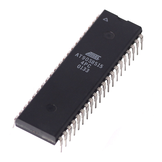
– 40-pin PDIP, 44-pin PLCC and TQFP
Operating Voltages
– 2.7 - 6.0V (AT90S4414-4 and AT90S8515-4)
– 4.0 - 6.0V (AT90S4414-8 and AT90S8515-8)
Speed Grades
– 0 - 4 MHz (AT90S4414-4 and AT90S8515-4)
– 0 - 8 MHz (AT90S4414-8 and AT90S8515-8)
Pin Configurations
8-bit
Microcontroller
with 4K/8K
bytes In-System
Programmable
Flash
AT90S4414
AT90S8515
Rev. 0841E–04/99
1

Advertisement

Table of Contents
loading
Need help?

Need help?

Do you have a question about the AT90S8515-8PI and is the answer not in the manual?

Questions and answers

Summary of Contents for Atmel AT90S8515-8PI

  • Page 1 Features ® • Utilizes the AVR RISC Architecture • AVR - High-performance and Low-power RISC Architecture – 118 Powerful Instructions - Most Single Clock Cycle Execution – 32 x 8 General Purpose Working Registers – Up to 8 MIPS Throughput at 8 MHz •...
  • Page 2: Block Diagram

    Description The AT90S4414/AT90S8515 is a low-power CMOS 8-bit microcontroller based on the AVR RISC architecture. By execut- ing powerful instructions in a single clock cycle, the AT90S4414/8515 achieves throughputs approaching 1 MIPS per MHz allowing the system designer to optimize power consumption versus processing speed. Block Diagram Figure 1.
  • Page 3: Pin Descriptions

    Flash allows the program memory to be reprogrammed in-system through an SPI serial interface or by a conventional nonvolatile memory programmer. By combining an enhanced RISC 8-bit CPU with In-System Programmable Flash on a monolithic chip, the Atmel AT90S4414/8515 is a powerful microcontroller that provides a highly flexible and cost effective solution to many embedded control applications.
  • Page 4: Crystal Oscillator

    Port B (PB7..PB0) Port B is an 8-bit bidirectional I/O port with internal pull-up resistors. The Port B output buffers can sink 20 mA. As inputs, Port B pins that are externally pulled low will source current if the pull-up resistors are activated. The Port B pins are tri-stated when a reset condition becomes active, even if the clock is not active.
  • Page 5: Architectural Overview

    AT90S4414/8515 Figure 2. Oscillator Connections MAX 1 HC BUFFER XTAL2 XTAL1 Note: When using the MCU Oscillator as a clock for an external device, an HC buffer should be connected as indicated in the figure. Figure 3. External Clock Drive Configuration Architectural Overview The fast-access register file concept contains 32 x 8-bit general purpose working registers with a single clock cycle access time.
  • Page 6 The AVR uses a Harvard architecture concept - with separate memories and buses for program and data. The program memory is executed with a two stage pipeline. While one instruction is being executed, the next instruction is pre-fetched from the program memory. This concept enables instructions to be executed in every clock cycle. The program memory is in-system programmable Flash memory.
  • Page 7 AT90S4414/8515 A flexible interrupt module has its control registers in the I/O space with an additional global interrupt enable bit in the status register. All the different interrupts have a separate interrupt vector in the interrupt vector table at the beginning of the p ro- gram memory.
  • Page 8: General Purpose Register File

    General Purpose Register File Figure 6 shows the structure of the 32 general purpose working registers in the CPU. Figure 6. AVR CPU General Purpose Working Registers Addr. … General Purpose Working Registers … X-register low byte X-register high byte Y-register low byte Y-register high byte Z-register low byte...
  • Page 9: Alu - Arithmetic Logic Unit

    AT90S4414/8515 ALU - Arithmetic Logic Unit The high-performance AVR ALU operates in direct connection with all the 32 general purpose working registers. Within a single clock cycle, ALU operations between registers in the register file are executed. The ALU operations are divided into three main categories - arithmetic, logical and bit-functions.
  • Page 10: Program And Data Addressing Modes

    The lower 352/608 Data Memory locations address the Register file, the I/O Memory and the internal data SRAM. The first 96 locations address the Register File + I/O Memory, and the next 256/512 locations address the internal data SRAM. An optional external data SRAM can be placed in the same SRAM memory space.
  • Page 11 AT90S4414/8515 Register Direct, Two Registers Rd and Rr Figure 10. Direct Register Addressing, two registers Operands are contained in register r (Rr) and d (Rd). The result is stored in register d (Rd). I/O Direct Figure 11. I/O Direct Addressing Operand address is contained in 6 bits of the instruction word.
  • Page 12 Data Direct Figure 12. Direct Data Addressing A 16-bit Data Address is contained in the 16 LSBs of a two-word instruction. Rd/Rr specify the destination or source register. Data Indirect with Displacement Figure 13. Data Indirect with Displacement Operand address is the result of the Y or Z-register contents added to the address contained in 6 bits of the instruction word.
  • Page 13 AT90S4414/8515 Data Indirect Figure 14. Data Indirect Addressing Operand address is the contents of the X, Y or the Z-register. Data Indirect with Pre-decrement Figure 15. Data Indirect Addressing with Pre-decrement The X, Y or the Z-register is decremented before the operation. Operand address is the decremented contents of the X, Y or the Z-register.
  • Page 14 Data Indirect with Post-increment Figure 16. Data Indirect Addressing with Post-increment The X, Y or the Z-register is incremented after the operation. Operand address is the content of the X, Y or the Z-register prior to incrementing. Constant Addressing Using the LPM Instruction Figure 17.
  • Page 15: Eeprom Data Memory

    AT90S4414/8515 Indirect Program Addressing, IJMP and ICALL Figure 18. Indirect Program Memory Addressing PROGRAM MEMORY $000 Z-REGISTER $7FF/$FFF Program execution continues at address contained by the Z-register (i.e. the PC is loaded with the contents of the Z-register). Relative Program Addressing, RJMP and RCALL Figure 19.
  • Page 16 Figure 20. The Parallel Instruction Fetches and Instruction Executions System Clock Ø 1st Instruction Fetch 1st Instruction Execute 2nd Instruction Fetch 2nd Instruction Execute 3rd Instruction Fetch 3rd Instruction Execute 4th Instruction Fetch Figure 21 shows the internal timing concept for the register file. In a single clock cycle an ALU operation using two register operands is executed, and the result is stored back to the destination register.
  • Page 17 AT90S4414/8515 I/O Memory The I/O space definition of the AT90S4414/8515 is shown in the following table: Table 2. AT90S4414/8515 I/O Space Address Hex Name Function $3F ($5F) SREG Status Register $3E ($5E) Stack Pointer High $3D ($5D) Stack Pointer Low $3B ($5B) GIMSK General Interrupt Mask register...
  • Page 18 Table 2. AT90S4414/8515 I/O Space (Continued) Address Hex Name Function $12 ($32) PORTD Data Register, Port D $11 ($31) DDRD Data Direction Register, Port D $10 ($30) PIND Input Pins, Port D $0F ($2F) SPDR SPI I/O Data Register $0E ($2E) SPSR SPI Status Register $0D ($2D)
  • Page 19: Reset And Interrupt Handling

    AT90S4414/8515 • Bit 5 - H: Half Carry Flag The half carry flag H indicates a half carry in some arithmetic operations. See the Instruction Set Description for detailed information. ⊕ • Bit 4 - S: Sign Bit, S = N The S-bit is always an exclusive or between the negative flag N and the two’s complement overflow flag V.
  • Page 20 Table 3. Reset and Interrupt Vectors Vector No. Program Address Source Interrupt Definition $000 RESET External Reset, Power-on Reset and Watchdog Reset $001 INT0 External Interrupt Request 0 $002 INT1 External Interrupt Request 1 $003 TIMER1 CAPT Timer/Counter1 Capture Event $004 TIMER1 COMPA Timer/Counter1 Compare Match A...
  • Page 21 AT90S4414/8515 Reset Sources The AT90S4414/8515 has three sources of reset: • Power-On Reset. The MCU is reset when the supply voltage is below the power-on reset threshold (V • External Reset. The MCU is reset when a low level is present on the RESET pin for more than 50 ns. •...
  • Page 22 Power-on Reset A Power-on Reset (POR) circuit ensures that the device is reset from power-on. As shown in Figure 23, an internal timer clocked from the Watchdog timer oscillator prevents the MCU from starting until after a certain period after V reached the Power-on Threshold voltage - V , regardless of the V rise time (see Figure 24).
  • Page 23 AT90S4414/8515 External Reset An external reset is generated by a low level on the RESET pin. Reset pulses longer than 50 ns will generate a reset, even if the clock is not running. Shorter pulses are not guaranteed to generate a reset. When the applied signal reaches the Reset Threshold Voltage - V on its positive edge, the delay timer starts the MCU after the Time-out period t TOUT...
  • Page 24 Interrupt Handling The AT90S4414/8515 has two 8-bit Interrupt Mask control registers; GIMSK - General Interrupt Mask register and TIMSK - Timer/Counter Interrupt Mask register. When an interrupt occurs, the Global Interrupt Enable I-bit is cleared (zero) and all interrupts are disabled. The user soft- ware can set (one) the I-bit to enable nested interrupts.
  • Page 25 AT90S4414/8515 • Bit 6 - INTF0: External Interrupt Flag0 When an event on the INT0 pin triggers an interrupt request, INTF0 becomes set (one). If the I-bit in SREG and the INT0 bit in GIMSK are set (one), the MCU will jump to the interrupt vector at address $001. The flag is cleared when the interrupt routine is executed.
  • Page 26 • Bit 6 - OCF1A: Output Compare Flag 1A The OCF1A bit is set (one) when compare match occurs between the Timer/Counter1 and the data in OCR1A - Output Compare Register 1A. OCF1A is cleared by hardware when executing the corresponding interrupt handling vector. Alterna- tively, OCF1A is cleared by writing a logic one to the flag.
  • Page 27 AT90S4414/8515 MCU Control Register - MCUCR The MCU Control Register contains control bits for general MCU functions. $35 ($55) ISC11 ISC10 ISC01 ISC00 MCUCR Read/Write Initial value • Bit 7 - SRE: External SRAM Enable When the SRE bit is set (one), the external data SRAM is enabled, and the pin functions AD0-7 (Port A), A8-15 (Port C), WR and RD (Port D) are activated as the alternate pin functions.
  • Page 28: Sleep Modes

    Table 7. Interrupt 0 Sense Control ISC01 ISC00 Description The low level of INT0 generates an interrupt request. Reserved The falling edge of INT0 generates an interrupt request. The rising edge of INT0 generates an interrupt request. Note: When changing the ISC01/ISC00 bits, INT0 must be disabled by clearing its Interrupt Enable bit in the GIMSK Register. Otherwise an interrupt can occur when the bits are changed.
  • Page 29: Timer/Counter Prescaler

    AT90S4414/8515 Timer/Counter Prescaler Figure 28 shows the general Timer/Counter prescaler. Figure 28. Timer/Counter Prescaler TCK1 TCK0 The four different prescaled selections are: CK/8, CK/64, CK/256 and CK/1024 where CK is the oscillator clock. For the two Timer/Counters, added selections as CK, external source and stop, can be selected as clock sources. 8-bit Timer/Counter0 Figure 29 shows the block diagram for Timer/Counter0.
  • Page 30 Figure 29. Timer/Counter0 Block Diagram Timer/Counter0 Control Register - TCCR0 $33 ($53) CS02 CS01 CS00 TCCR0 Read/Write Initial value • Bits 7..3 - Res: Reserved bits These bits are reserved bits in the AT90S4414/8515 and always read as zero. • Bits 2,1,0 - CS02, CS01, CS00: Clock Select0, bit 2,1 and 0 The Clock Select0 bits 2,1 and 0 define the prescaling source of Timer/Counter0.
  • Page 31 AT90S4414/8515 The Stop condition provides a Timer Enable/Disable function. The CK down divided modes are scaled directly from the CK oscillator clock. If the external pin modes are used for Timer/Counter0, transitions on PB0/(T0) will clock the counter even if the pin is configured as an output.
  • Page 32 The 16-bit Timer/Counter1 can select clock source from CK, prescaled CK, or an external pin. In addition it can be stopped as described in the specification for the Timer/Counter1 Control Registers - TCCR1A and TCCR1B. The different status flags (overflow, compare match and capture event) are found in the Timer/Counter Interrupt Flag Register - TIFR. Control signals are found in the Timer/Counter1 Control Registers - TCCR1A and TCCR1B.
  • Page 33 AT90S4414/8515 Table 9. Compare 1 Mode Select COM1X1 COM1X0 Description Timer/Counter1 disconnected from output pin OC1X Toggle the OC1X output line. Clear the OC1X output line (to zero). Set the OC1X output line (to one). Note: X = A or B In PWM mode, these bits have a different function.
  • Page 34 • Bit 3 - CTC1: Clear Timer/Counter1 on Compare Match When the CTC1 control bit is set (one), the Timer/Counter1 is reset to $0000 in the clock cycle after a compareA match. If the CTC1 control bit is cleared, Timer/Counter1 continues counting and is unaffected by a compare match. Since the compare match is detected in the CPU clock cycle following the match, this function will behave differently when a prescal- ing higher than 1 is used for the timer.
  • Page 35 AT90S4414/8515 • TCNT1 Timer/Counter1 Read: When the CPU reads the low byte TCNT1L, the data of the low byte TCNT1L is sent to the CPU and the data of the high byte TCNT1H is placed in the TEMP register. When the CPU reads the data in the high byte TCNT1H, the CPU receives the data in the TEMP register.
  • Page 36 Timer/Counter1 Input Capture Register - ICR1H AND ICR1L $25 ($45) ICR1H $24 ($44) ICR1L Read/Write Initial value The input capture register is a 16-bit read-only register. When the rising or falling edge (according to the input capture edge setting - ICES1) of the signal at the input capture pin - ICP - is detected, the current value of the Timer/Counter1 is transferred to the Input Capture Register - ICR1.
  • Page 37 AT90S4414/8515 Note that in the PWM mode, the 10 least significant OCR1A/OCR1B bits, when written, are transferred to a temporary loca- tion. They are latched when Timer/Counter1 reaches the value TOP. This prevents the occurrence of odd-length PWM pulses (glitches) in the event of an unsynchronized OCR1A/OCR1B write. See Figure 32 for an example. Figure 32.
  • Page 38: Watchdog Timer

    Watchdog Timer The Watchdog Timer is clocked from a separate on-chip oscillator which runs at 1MHz. This is the typical value at V 5V. See characterization data for typical values at other V levels. By controlling the Watchdog Timer prescaler, the Watchdog reset interval can be adjusted, see Table 15 for a detailed description.
  • Page 39: Eeprom Read/Write Access

    AT90S4414/8515 • Bits 2..0 - WDP2, WDP1, WDP0: Watch Dog Timer Prescaler 2, 1 and 0 The WDP2, WDP1 and WDP0 bits determine the Watchdog Timer prescaling when the Watchdog Timer is enabled. The different prescaling values and their corresponding Time-out Periods are shown in Table 15. Table 15.
  • Page 40 EEPROM Data Register - EEDR $1D ($3D) EEDR Read/Write Initial value • Bits 7..0 - EEDR7..0: EEPROM Data For the EEPROM write operation, the EEDR register contains the data to be written to the EEPROM in the address given by the EEAR register. For the EEPROM read operation, the EEDR contains the data read out from the EEPROM at the address given by EEAR.
  • Page 41: Prevent Eeprom Corruption

    AT90S4414/8515 • Bit 0 - EERE: EEPROM Read Enable The EEPROM Read Enable Signal EERE is the read strobe to the EEPROM. When the correct address is set up in the EEAR register, the EERE bit must be set. When the EERE bit is cleared (zero) by hardware, requested data is found in the EEDR register.
  • Page 42 Figure 34. SPI Block Diagram The interconnection between master and slave CPUs with SPI is shown in Figure 35. The PB7(SCK) pin is the clock output in the master mode and is the clock input in the slave mode. Writing to the SPI data register of the master CPU starts the SPI clock generator, and the data written shifts out of the PB5(MOSI) pin and into the PB5(MOSI) pin of the slave CPU.
  • Page 43: Ss Pin Functionality

    AT90S4414/8515 Figure 35. SPI Master-slave Interconnection The system is single buffered in the transmit direction and double buffered in the receive direction. This means that bytes to be transmitted cannot be written to the SPI Data Register before the entire shift cycle is completed. When receiving data, however, a received byte must be read from the SPI Data Register before the next byte has been completely shifted in.
  • Page 44: Data Modes

    Data Modes There are four combinations of SCK phase and polarity with respect to serial data, which are determined by control bits CPHA and CPOL. The SPI data transfer formats are shown in Figure 36 and Figure 37. Figure 36. SPI Transfer Format with CPHA = 0 and DORD = 0 Figure 37.
  • Page 45 AT90S4414/8515 • Bit 3 - CPOL: Clock Polarity When this bit is set (one), SCK is high when idle. When CPOL is cleared (zero), SCK is low when idle. Refer to Figure 36 and Figure 37 for additional information. • Bit 2 - CPHA: Clock Phase Refer to Figure 36 or Figure 37 for the functionality of this bit.
  • Page 46: Data Transmission

    UART The AT90S4414/8515 features a full duplex (separate receive and transmit registers) Universal Asynchronous Receiver and Transmitter (UART). The main features are: • Baud rate generator that can generate a large number of baud rates (bps) • High baud rates at low XTAL frequencies •...
  • Page 47: Data Reception

    AT90S4414/8515 Data transmission is initiated by writing the data to be transmitted to the UART I/O Data Register, UDR. Data is transferred from UDR to the Transmit shift register when: • A new character has been written to UDR after the stop bit from the previous character has been shifted out. The shift register is loaded immediately.
  • Page 48: Uart Control

    The receiver front-end logic samples the signal on the RXD pin at a frequency 16 times the baud rate. While the line is idle, one single sample of logical zero will be interpreted as the falling edge of a start bit, and the start bit detection sequence is initiated.
  • Page 49 AT90S4414/8515 UART Status Register - USR $0B ($2B) UDRE Read/Write Initial value The USR register is a read-only register providing information on the UART Status. • Bit 7 - RXC: UART Receive Complete This bit is set (one) when a received character is transferred from the Receiver Shift register to UDR. The bit is set regard- less of any detected framing errors.
  • Page 50 • Bit 5 - UDRIE: UART Data Register Empty Interrupt Enable When this bit is set (one), a setting of the UDRE bit in USR will cause the UART Data Register Empty interrupt routine to be executed provided that global interrupts are enabled. •...
  • Page 51 AT90S4414/8515 Table 18. UBRR Settings at Various Crystal Frequencies Baud Rate 1 MHz %Error 1.8432 MHz %Error 2 MHz %Error 2.4576 MHz %Error 2400 UBRR= 0.2 UBRR= 0.0 UBRR= 0.2 UBRR= 4800 UBRR= 0.2 UBRR= 0.0 UBRR= 0.2 UBRR= 9600 UBRR= 7.5 UBRR= 0.0 UBRR= 0.2 UBRR=...
  • Page 52: Analog Comparator

    Analog Comparator The analog comparator compares the input values on the positive input PB2 (AIN0) and negative input PB3 (AIN1). When the voltage on the positive input PB2 (AIN0) is higher than the voltage on the negative input PB3 (AIN1), the Analog Com- parator Output, ACO is set (one).
  • Page 53 AT90S4414/8515 • Bit 2 - ACIC: Analog Comparator Input Capture Enable When set (one), this bit enables the Input Capture function in Timer/Counter1 to be triggered by the analog comparator. The comparator output is in this case directly connected to the Input Capture front-end logic, making the comparator utilize the noise canceler and edge select features of the Timer/Counter1 Input Capture interrupt.
  • Page 54 Figure 42. External SRAM Connected to the AVR D[7:0] Port A A[7:0] SRAM A[15:8] Port C Figure 43. External Data SRAM Memory Cycles without Wait State System Clock Ø Address [15..8] Prev. Address Address Data / Address [7..0] Prev. Address Address Data Address...
  • Page 55 AT90S4414/8515 I/O-Ports All AVR ports have true Read-Modify-Write functionality when used as general digital I/O ports. This means that the direc- tion of one port pin can be changed without unintentionally changing the direction of any other pin with the SBI and CBI instructions.
  • Page 56 Table 20. DDAn Effects on Port A Pins DDAn PORTAn Pull up Comment Input Tri-state (Hi-Z) Input PAn will source current if ext. pulled low. Output Push-Pull Zero Output Output Push-Pull One Output n: 7,6…0, pin number. Port A Schematics Note that all port pins are synchronized.
  • Page 57 AT90S4414/8515 Port B Port B is an 8-bit bi-directional I/O port. Three I/O memory address locations are allocated for the Port B, one each for the Data Register - PORTB, $18($38), Data Direction Register - DDRB, $17($37) and the Port B Input Pins - PINB, $16($36). The Port B Input Pins address is read only, while the Data Register and the Data Direction Register are read/write.
  • Page 58 PortB as General Digital I/O All 8 pins in port B have equal functionality when used as digital I/O pins. PBn, General I/O pin: The DDBn bit in the DDRB register selects the direction of this pin, if DDBn is set (one), PBn is con- figured as an output pin.
  • Page 59 AT90S4414/8515 Port B Schematics Note that all port pins are synchronized. The synchronization latches are however, not shown in the figures. Figure 46. Port B Schematic Diagram (Pins PB0 and PB1) PULL- RESET DDBn RESET PORTBn WRITE PORTB TIMERn CLOCK SENSE CONTROL WRITE DDRB SOURCE MUX...
  • Page 60 Figure 48. Port B Schematic Diagram (Pin PB4) PULL- RESET DDB4 RESET PORTB4 MSTR WRITE PORTB WRITE DDRB READ PORTB LATCH READ PORTB PIN READ DDRB MSTR: SPI MASTER ENABLE SPI SS SPE: SPI ENABLE Figure 49. Port B Schematic Diagram (Pin PB5) PULL- RESET DDB5...
  • Page 61 AT90S4414/8515 Figure 50. Port B Schematic Diagram (Pin PB6) PULL- RESET DDB6 RESET PORTB6 WRITE PORTB MSTR WRITE DDRB READ PORTB LATCH SPI SLAVE READ PORTB PIN READ DDRB SPE: SPI ENABLE MSTR MASTER SELECT SPI MASTER Figure 51. Port B Schematic Diagram (Pin PB7) PULL- RESET DDB7...
  • Page 62 Port C Port C is an 8-bit bi-directional I/O port. Three I/O memory address locations are allocated for the Port C, one each for the Data Register - PORTC, $15($35), Data Direction Register - DDRC, $14($34) and the Port C Input Pins - PINC, $13($33). The Port C Input Pins address is read only, while the Data Register and the Data Direction Register are read/write.
  • Page 63 AT90S4414/8515 Port C Schematics Note that all port pins are synchronized. The synchronization latch is however, not shown in the figure. Figure 52. Port C Schematic Diagram (Pins PC0 - PC7) Port D Port D is an 8 bit bi-directional I/O port with internal pull-up resistors. Three I/O memory address locations are allocated for the Port D, one each for the Data Register - PORTD, $12($32), Data Direction Register - DDRD, $11($31) and the Port D Input Pins - PIND, $10($30).
  • Page 64 Port D Data Register - PORTD $12 ($32) PORTD7 PORTD6 PORTD5 PORTD4 PORTD3 PORTD2 PORTD1 PORTD0 PORTD Read/Write Initial value Port D Data Direction Register - DDRD $11 ($31) DDD7 DDD6 DDD5 DDD4 DDD3 DDD2 DDD1 DDD0 DDRD Read/Write Initial value Port D Input Pins Address - PIND $10 ($30) PIND7...
  • Page 65 AT90S4414/8515 • INT1 - Port D, Bit 3 INT1, External Interrupt source 1: The PD3 pin can serve as an external interrupt source to the MCU. See the interrupt description for further details, and how to enable the source. • INT0 - Port D, Bit 2 INT0, External Interrupt source 0: The PD2 pin can serve as an external interrupt source to the MCU.
  • Page 66 Figure 54. Port D Schematic Diagram (Pin PD1) PULL- RESET DDD1 RESET PORTD1 WRITE PORTD WRITE DDRD TXEN READ PORTD LATCH READ PORTD PIN READ DDRD UART TRANSMIT DATA TXD: TXEN: UART TRANSMIT ENABLE Figure 55. Port D Schematic Diagram (Pins PD2 and PD3) AT90S4414/8515...
  • Page 67 AT90S4414/8515 Figure 56. Port D Schematic Diagram (Pin PD4) Figure 57. Port D Schematic Diagram (Pin PD5)
  • Page 68 Figure 58. Port D Schematic Diagram (Pin PD6) Figure 59. Port D Schematic Diagram (Pin PD7) AT90S4414/8515...
  • Page 69: Memory Programming

    The Fuse bits are not accessible in Serial Programming Mode. The status of the Fuse bits is not affected by Chip Erase. Signature Bytes All Atmel microcontrollers have a three-byte signature code which identifies the device. This code can be read in both serial and parallel mode. The three bytes reside in a separate address space.
  • Page 70: Parallel Programming

    The Program and Data memory arrays on the AT90S4414/8515 are programmed byte-by-byte in either programming modes. For the EEPROM, an auto-erase cycle is provided within the self-timed write operation in the serial programming mode. During programming, the supply voltage must be in accordance with Table 27. Table 27.
  • Page 71 AT90S4414/8515 Table 28. Pin Name Mapping Signal Name in Programming Mode Pin Name Function RDY/BSY 0: Device is busy programming, 1: Device is ready for new command Output Enable (Active low) Write Pulse (Active low) Byte Select (“0” selects low byte, “1” selects high byte) XTAL Action Bit 0 XTAL Action Bit 1 DATA...
  • Page 72 Chip Erase The Chip Erase command will erase the Flash and EEPROM memories, and the Lock bits. The Lock bits are not reset until the Flash and EEPROM have been completely erased. The Fuse bits are not changed. Chip Erase must be performed before the Flash or EEPROM is reprogrammed.
  • Page 73 AT90S4414/8515 3. Wait until RDY/BSY goes high to program the next byte. (See Figure 62 for signal waveforms.) The loaded command and address are retained in the device during programming. For efficient programming, the following should be considered. • The command needs only be loaded once when writing or reading multiple memory locations. •...
  • Page 74 Reading the Flash The algorithm for reading the Flash memory is as follows (refer to Programming the Flash for details on Command and Address loading): 1. A: Load Command “0000 0010”. 2. B: Load Address High Byte ($00 - $07/$0F). 3.
  • Page 75 AT90S4414/8515 Programming the Lock Bits The algorithm for programming the Lock bits is as follows (refer to Programming the Flash for details on Command and Data loading): 1. A: Load Command “0010 0000”. 2. D: Load Data Low Byte. Bit n = ‘0’ programs the Lock bit. Bit 2 = Lock Bit2 Bit 1 = Lock Bit1 Bit 7-3,0 = “1”.
  • Page 76: Parallel Programming Characteristics

    Parallel Programming Characteristics Figure 63. Parallel Programming Timing XLWL XTAL1 XHXL DVXH XLDX BVWL Data & Contol (DATA, XA0/1, BS) WLWH RHBX WHRL RDY/BSY WLRH XLOL OHDZ OLDV DATA Table 31. Parallel Programming Characteristics T = 25°C ± 10%, V =5V ±...
  • Page 77: Serial Downloading

    AT90S4414/8515 Serial Downloading Both the Program and Data memory arrays can be programmed using the SPI bus while RESET is pulled to GND. The serial interface consists of pins SCK, MOSI (input) and MISO (output), see Figure 64. After RESET is set low, the Program- ming Enable instruction needs to be executed first before program/erase instructions can be executed.
  • Page 78 Serial Programming Algorithm When writing serial data to the AT90S4414/8515, data is clocked on the rising edge of SCK. When reading data from the AT90S4414/8515, data is clocked on the falling edge of SCK. See Figure 65, Figure 66 and Table 34 for timing details.
  • Page 79 AT90S4414/8515 Data Polling Flash When a byte is being programmed into the Flash, reading the address location being programmed will give the value $7F. At the time the device is ready for a new byte, the programmed value will read correctly. This is used to determine when the next byte can be written.
  • Page 80: Serial Programming Characteristics

    Serial Programming Characteristics Figure 66. Serial Programming Timing MOSI SLSH OVSH SHOX SHSL MISO SLIV Table 34. Serial Programming Characteristics, T = -40°C to 85°C, V = 2.7 - 6.0V (Unless otherwise noted) Symbol Parameter Units Oscillator Frequency (V = 2.7 - 4.0V) CLCL Oscillator Period (V = 2.7 - 4.0V)
  • Page 81: Electrical Characteristics

    AT90S4414/8515 Electrical Characteristics Absolute Maximum Ratings* *NOTICE: Stresses beyond those listed under “Absolute Operating Temperature........-55°C to +125°C Maximum Ratings” may cause permanent dam- age to the device. This is a stress rating only and Storage Temperature ........-65°C to +150°C functional operation of the device at these or Voltage on any Pin except RESET other conditions beyond those indicated in the...
  • Page 82 DC Characteristics = -40°C to 85°C, V = 2.7V to 6.0V (unless otherwise noted) Symbol Parameter Condition Units Input Low Voltage (Except XTAL1) -0.5 Input Low Voltage (XTAL1) -0.5 Input High Voltage (Except XTAL1, RESET) 0.6 V + 0.5 Input High Voltage (XTAL1) 0.8 V + 0.5...
  • Page 83: External Clock Drive Waveforms

    AT90S4414/8515 External Clock Drive Waveforms Figure 67. External Clock VIH1 VIL1 Table 37. External Clock Drive = 2.7V to 4.0V = 4.0V to 6.0V Symbol Parameter Units Oscillator Frequency CLCL Clock Period CLCL High Time CHCX Low Time CLCX Rise Time µs CLCH Fall Time...
  • Page 84: External Data Memory Timing

    External Data Memory Timing Table 38. External Data Memory Characteristics, 4.0 - 6.0 Volts, No Wait State 8 MHz Oscillator Variable Oscillator Symbol Parameter Unit Oscillator Frequency CLCL ALE Pulse Width 32.5 0.5t -30.0 LHLL CLCL Address Valid A to ALE Low 22.5 0.5t -40.0...
  • Page 85 AT90S4414/8515 Table 40. External Data Memory Characteristics, 2.7 - 4.0 Volts, No Wait State 4 MHz Oscillator Variable Oscillator Symbol Parameter Unit Oscillator Frequency CLCL ALE Pulse Width 70.0 0.5t -55.0 LHLL CLCL Address Valid A to ALE Low 60.0 0.5t -65.0 AVLL...
  • Page 86: Typical Characteristics

    Typical Characteristics The following charts show typical behavior. These data are characterized, but not tested. All current consumption measure- ments are performed with all I/O pins configured as inputs and with internal pull-ups enabled. ICP pulled high externally. A sine wave generator with rail to rail output is used as clock source. The power consumption in power-down mode is independent of clock selection.
  • Page 87 AT90S4414/8515 Figure 70. Active Supply Current vs. V ACTIVE SUPPLY CURRENT vs. V FREQUENCY = 4 MHz T = -40 ˚ T = 25 ˚ T = 85 ˚ Figure 71. Idle Supply Current vs. Frequency IDLE SUPPLY CURRENT vs. FREQUENCY T = 25˚C = 6V = 5.5V...
  • Page 88 Figure 72. Idle Supply current vs. V IDLE SUPPLY CURRENT vs. V FREQUENCY = 4 MHz T = -40 ˚ T = 25 ˚ T = 85 ˚ Figure 73. Power Down Supply Current vs. V POWER DOWN SUPPLY CURRENT vs. V WATCHDOG TIMER DISABLED T = 85 ˚...
  • Page 89 AT90S4414/8515 Figure 74. Power Down Supply Current vs. V POWER DOWN SUPPLY CURRENT vs. V WATCHDOG TIMER ENABLED T = 85 ˚ T = 25 ˚ Figure 75. Analog Comparator Current vs. V ANALOG COMPARATOR CURRENT vs. V T = 25 ˚...
  • Page 90 Analog comparator offset voltage is measured as absolute offset Figure 76. Analog Comparator Offest Voltage vs. Common Mode Voltage ANALOG COMPARATOR OFFSET VOLTAGE vs. COMMON MODE VOLTAGE V = 5V T = 25 ˚ T = 85 ˚ Common Mode Voltage (V) Figure 77.
  • Page 91 AT90S4414/8515 Figure 78. Analog Comparator Input Leakage Current ANALOG COMPARATOR INPUT LEAKAGE CURRENT V = 6V T = 25 ˚ V (V) Figure 79. Watchdog Oscillator Frequency vs. V WATCHDOG OSCILLATOR FREQUENCY vs. V 1600 T = 25 ˚ 1400 T = 85 ˚...
  • Page 92 Sink and source capabilities of I/O ports are measured on one pin at a time. Figure 80. Pull-up Resistor Current vs. Input Voltage PULL-UP RESISTOR CURRENT vs. INPUT VOLTAGE V = 5V T = 25 ˚ T = 85 ˚ Figure 81.
  • Page 93 AT90S4414/8515 Figure 82. I/O Pin Sink Current vs. Output Voltage I/O PIN SINK CURRENT vs. OUTPUT VOLTAGE V = 5V T = 25 ˚ T = 85 ˚ Figure 83. I/O Pin Source Current vs. Output Voltage I/O PIN SOURCE CURRENT vs. OUTPUT VOLTAGE V = 5V T = 25 ˚...
  • Page 94 Figure 84. I/O Pin Source Curent vs. Output Voltage I/O PIN SOURCE CURRENT vs. OUTPUT VOLTAGE V = 2.7V T = 25 ˚ T = 85 ˚ Figure 85. I/O Pin Input Threshold Voltage vs. V I/O PIN INPUT THRESHOLD VOLTAGE vs. V T = 25 ˚...
  • Page 95 AT90S4414/8515 Figure 86. I/O Pin Input Hysteresis vs. V I/O PIN INPUT HYSTERESIS vs. V T = 25 ˚ 0.18 0.16 0.14 0.12 0.08 0.06 0.04 0.02 Figure 87. I/O Pin Sink Current vs. Output Voltage I/O PIN SINK CURRENT vs. OUTPUT VOLTAGE V = 2.7V T = 25 ˚...
  • Page 96: Register Summary

    Register Summary Address Name Bit 7 Bit 6 Bit 5 Bit 4 Bit 3 Bit 2 Bit 1 Bit 0 Page $3F ($5F) SREG $3E ($5E) SP15 SP14 SP13 SP12 SP11 SP10 $3D ($5D) $3C ($5C) Reserved $3B ($5B) GIMSK INT1 INT0 $3A ($5A)
  • Page 97: Instruction Set Summary

    AT90S4414/8515 Instruction Set Summary Mnemonics Operands Description Operation Flags #Clocks ARITHMETIC AND LOGIC INSTRUCTIONS Rd ← Rd + Rr Rd, Rr Add two Registers Z,C,N,V,H Rd ← Rd + Rr + C Rd, Rr Add with Carry two Registers Z,C,N,V,H Rdh:Rdl ←...
  • Page 98 Instruction Set Summary (Continued) Mnemonics Operands Description Operation Flags #Clocks DATA TRANSFER INSTRUCTIONS Rd ← Rr Rd, Rr Move Between Registers None Rd ← K Rd, K Load Immediate None Rd ← (X) Rd, X Load Indirect None Rd ← (X), X ← X + 1 Rd, X+ Load Indirect and Post-Inc.
  • Page 99: Ordering Information

    (0°C to 70°C) AT90S8515-8PC 40P6 AT90S8515-8AI Industrial AT90S8515-8JI (-40°C to 85°C) AT90S8515-8PI 40P6 Note: Order AT90S8515A-XXX for devices with the FSTRT Fuse programmed. Package Type 44-lead, Thin (1.0 mm) Plastic Gull Wing Quad Flat Package (TQFP) 44-lead, Plastic J-leaded Chip Carrier (PLCC) 40P6 40-lead, 0.600"...
  • Page 100: Packaging Information

    Packaging Information 44A, 44-lead, Thin (1.0 mm) Plastic Gull Wing Quad 44J, 44-lead, Plastic J-leaded Chip Carrier (PLCC) Flat Package (TQFP) Dimensions in Inches and (Millimeters) Dimensions in Millimeters and (Inches)* .045(1.14) X 30° - 45° 12.21(0.478) .045(1.14) X 45° PIN NO.
  • Page 101 No licenses to patents or other intellectual prop- erty of Atmel are granted by the Company in connection with the sale of Atmel products, expressly or by implication. Atmel’s products are not authorized for use as critical components in life suppor t devices or systems.

Table of Contents