Table of Contents
Advertisement
Quick Links
Features
•
High-performance and Low-power AVR
– 118 Powerful Instructions - Most Single Cycle Execution
– 32 x 8 General Purpose Working Registers
– Up to 8 MIPS Throughput at 8 MHz
•
Data and Nonvolatile Program Memory
– 2K/4K Bytes of In-System Programmable Flash
Endurance 1,000 Write/Erase Cycles
– 128 Bytes of SRAM
– 128/256 Bytes of In-System Programmable EEPROM
Endurance: 100,000 Write/Erase Cycles
– Programming Lock for Flash Program and EEPROM Data Security
•
Peripheral Features
– One 8-bit Timer/Counter with Separate Prescaler
– Expanded 16-bit Timer/Counter with Separate Prescaler,
Compare, Capture Modes and 8-, 9- or 10-bit PWM
– On-chip Analog Comparator
– Programmable Watchdog Timer with Separate On-chip Oscillator
– Programmable UART
– 6-channel, 10-bit ADC
– Master/Slave SPI Serial Interface
•
Special Microcontroller Features
– Brown-Out Reset Circuit
– Enhanced Power-on Reset Circuit
– Low-Power Idle and Power Down Modes
– External and Internal Interrupt Sources
•
Specifications
– Low-power, High-speed CMOS Process Technology
– Fully Static Operation
•
Power Consumption at 4 MHz, 3V, 25°C
– Active: 3.4 mA
– Idle Mode: 1.4 mA
– Power Down Mode: <1 µA
•
I/O and Packages
– 20 Programmable I/O Lines
– 28-pin PDIP and 32-pin TQFP
•
Operating Voltage
– 2.7V - 6.0V (AT90LS2333 and AT90LS4433)
– 4.0V - 6.0V (AT90S2333 and AT90S4433)
•
Speed Grades
– 0 - 4 MHz (AT90LS2333 and AT90LS4433)
– 0 - 8 MHz (AT90S2333 and AT90S4433)
Pin Configurations
TQFP Top View
(INT1) PD3
1
(T0) PD4
2
NC
3
VCC
4
GND
5
NC
6
XTAL1
7
XTAL2
8
®
8-bit RISC Architecture
(RXD) PD0
(TXD) PD1
(INT0) PD2
(INT1) PD3
24
PC1 (ADC1)
23
PC0 (ADC0)
22
NC
21
AGND
20
AREF
19
NC
18
AVCC
17
PB5 (SCK)
(AIN0) PD6
(AIN1) PD7
PDIP
RESET
1
28
PC5 (ADC5)
2
27
PC4 (ADC4)
3
26
PC3 (ADC3)
4
25
PC2 (ADC2)
5
24
PC1 (ADC1)
(T0) PD4
6
23
PC0 (ADC0)
VCC
7
22
AGND
GND
8
21
AREF
XTAL1
9
20
AVCC
XTAL2
10
19
PB5 (SCK)
(T1) PD5
11
18
PB4 (MISO)
12
17
PB3 (MOSI)
13
16
PB2 (SS)
(ICP) PB0
14
15
PB1 (OC1)
8-bit
Microcontroller
with 2K/4K bytes
In-System
Programmable
Flash
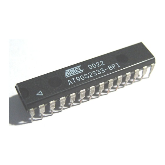
AT90S2333
AT90LS2333
AT90S4433
AT90LS4433
Preliminary
Rev. 1042D–04/99
1
Advertisement
Table of Contents


Need help?
Do you have a question about the AVR AT90S2333 and is the answer not in the manual?
Questions and answers