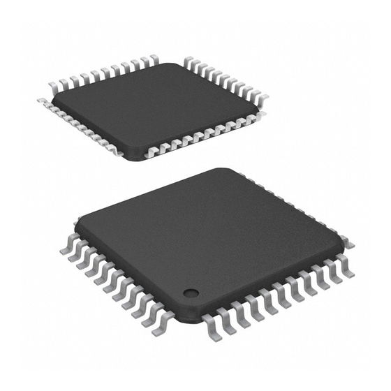
Atmel AVR AT90S4434 Preliminary

Atmel AVR AT90S4434 Preliminary

8-bit microcontroller with 4k/8k bytes in-system programmable flash

Advertisement

Features
®
AVR
– High-performance and Low-power RISC Architecture
– 118 Powerful Instructions – Most Single Clock Cycle Execution
– 32 x 8 General-purpose Working Registers
– Up to 8 MIPS Throughput at 8 MHz
Data and Nonvolatile Program Memories
– 4K/8K Bytes of In-System Programmable Flash
SPI Serial Interface for In-System Programming
Endurance: 1,000 Write/Erase Cycles
– 256/512 Bytes EEPROM
Endurance: 100,000 Write/Erase Cycles
– 256/512 Bytes Internal SRAM
– Programming Lock for Software Security
Peripheral Features
– 8-channel, 10-bit ADC
– Programmable UART
– Master/Slave SPI Serial Interface
– Two 8-bit Timer/Counters with Separate Prescaler and Compare Mode
– One 16-bit Timer/Counter with Separate Prescaler, Compare and
Capture Modes and Dual 8-, 9- or 10-bit PWM
– Programmable Watchdog Timer with On-chip Oscillator
– On-chip Analog Comparator
Special Microcontroller Features
– Power-on Reset Circuit
– Real-time Clock (RTC) with Separate Oscillator and Counter Mode
– External and Internal Interrupt Sources
– Three Sleep Modes: Idle, Power Save and Power-down
Power Consumption at 4 MHz, 3V, 20°C
– Active: 6.4 mA
– Idle Mode: 1.9 mA
– Power-down Mode: <1 µA
I/O and Packages
– 32 Programmable I/O Lines
– 40-pin PDIP, 44-pin PLCC and 44-pin TQFP
Operating Voltages
– V
: 4.0 - 6.0V AT90S4434/AT90S8535
CC
– V
: 2.7 - 6.0V AT90LS4434/AT90LS8535
CC
Speed Grades:
– 0 - 8 MHz AT90S4434/AT90S8535
– 0 - 4 MHz AT90LS4434/AT90LS8535
Pin Configurations
8-bit
Microcontroller
with 4K/8K
Bytes In-System
Programmable
Flash
AT90S4434
AT90LS4434
AT90S8535
AT90LS8535
Preliminary
Rev. 1041F–10/00
1

Advertisement

Table of Contents
loading
Need help?

Need help?

Do you have a question about the AVR AT90S4434 and is the answer not in the manual?

Questions and answers

Subscribe to Our Youtube Channel

Summary of Contents for Atmel AVR AT90S4434

  • Page 1 Features ® • – High-performance and Low-power RISC Architecture – 118 Powerful Instructions – Most Single Clock Cycle Execution – 32 x 8 General-purpose Working Registers – Up to 8 MIPS Throughput at 8 MHz • Data and Nonvolatile Program Memories –...
  • Page 2: Block Diagram

    Description The AT90S4434/8535 is a low-power CMOS 8-bit microcontroller based on the AVR RISC architecture. By executing pow- erful instructions in a single clock cycle, the AT90S4434/8535 achieves throughputs approaching 1 MIPS per MHz allowing the system designer to optimize power consumption versus processing speed. Block Diagram Figure 1.
  • Page 3: Pin Descriptions

    SPI serial interface or by a conventional nonvolatile memory programmer. By combining an 8-bit RISC CPU with In-System Programmable Flash on a monolithic chip, the Atmel AT90S4434/8535 is a powerful microcontroller that provides a highly flexible and cost effective solution to many embedded control applications.
  • Page 4 The Port B pins are tri-stated when a reset condition becomes active, even if the clock is not running. Port C (PC7..PC0) Port C is an 8-bit bi-directional I/O port with internal pull-up resistors. The Port C output buffers can sink 20 mA. As inputs, Port C pins that are externally pulled low will source current if the pull-up resistors are activated.
  • Page 5: Clock Options

    AT90S/LS4434 and AT90S/LS8535 Clock Options Crystal Oscillator XTAL1 and XTAL2 are input and output, respectively, of an inverting amplifier which can be configured for use as an on-chip oscillator, as shown in Figure 2. Either a quartz crystal or a ceramic resonator may be used. Figure 2.
  • Page 6: Architectural Overview

    One of the three address pointers is also used as the address pointer for the constant table look-up function. These added function registers are the 16-bit X-register, Y-register and Z-register. Figure 4. The AT90S4434/8535 AVR RISC Architecture AVR AT90S4434/8535 Architecture Data Bus 8-bit Program...
  • Page 7 AT90S/LS4434 and AT90S/LS8535 The I/O memory space contains 64 addresses for CPU peripheral functions as Control Registers, Timer/Counters, A/D converters and other I/O functions. The I/O memory can be accessed directly or as the Data Space locations following those of the register file, $20 - $5F. The AVR uses a Harvard architecture concept –...
  • Page 8: General-Purpose Register File

    General-purpose Register File Figure 6 shows the structure of the 32 general-purpose working registers in the CPU. Figure 6. AVR CPU General-purpose Working Registers Addr. … General Purpose Working Registers … X-register low byte X-register high byte Y-register low byte Y-register high byte Z-register low byte Z-register high byte...
  • Page 9: Alu - Arithmetic Logic Unit

    AT90S/LS4434 and AT90S/LS8535 ALU – Arithmetic Logic Unit The high-performance AVR ALU operates in direct connection with all the 32 general-purpose working registers. Within a single clock cycle, ALU operations between registers in the register file are executed. The ALU operations are divided into three main categories: arithmetic, logical and bit functions.
  • Page 10: Program And Data Addressing Modes

    When using register indirect addressing modes with automatic pre-decrement and post-increment, the address registers X, Y and Z are decremented and incremented. The 32 general-purpose working registers, 64 I/O registers and the 256/512 bytes of internal data SRAM in the AT90S4434/8535 are all accessible through all these addressing modes.
  • Page 11 AT90S/LS4434 and AT90S/LS8535 I/O Direct Figure 11. I/O Direct Addressing Operand address is contained in six bits of the instruction word. n is the destination or source register address. Data Direct Figure 12. Direct Data Addressing Data Space $0000 20 19 Rr/Rd 16 LSBs $015F/...
  • Page 12: Data Indirect With Pre-Decrement

    Data Indirect Figure 14. Data Indirect Addressing Data Space $0000 X, Y OR Z - REGISTER $015F/ $025F Operand address is the contents of the X-, Y- or the Z-register. Data Indirect with Pre-decrement Figure 15. Data Indirect Addressing with Pre-decrement Data Space $0000 X, Y OR Z - REGISTER...
  • Page 13 AT90S/LS4434 and AT90S/LS8535 Constant Addressing Using the LPM Instruction Figure 17. Code Memory Constant Addressing $7FF/ $FFF Constant byte address is specified by the Z-register contents. The 15 MSBs select word address (0 - 2K/4K), the LSB selects low byte if cleared (LSB = 0) or high byte if set (LSB = 1). Indirect Program Addressing, IJMP and ICALL Figure 18.
  • Page 14: Eeprom Data Memory

    Relative Program Addressing, RJMP and RCALL Figure 19. Relative Program Memory Addressing $7FF/ $FFF Program execution continues at address PC + k + 1. The relative address k is from -2048 to 2047. EEPROM Data Memory The AT90S4434/8535 contains 256/512 bytes of data EEPROM memory. It is organized as a separate data space, in which single bytes can be read and written.
  • Page 15 AT90S/LS4434 and AT90S/LS8535 Figure 21. Single Cycle ALU Operation System Clock Ø Total Execution Time Register Operands Fetch ALU Operation Execute Result Write Back The internal data SRAM access is performed in two System Clock cycles as described in Figure 22. Figure 22.
  • Page 16 I/O Memory The I/O space definition of the AT90S4434/8535 is shown in Table 2. Table 2. AT90S4434/8535 I/O Space I/O Address (SRAM Address) Name Function $3F ($5F) SREG Status REGister $3E ($5E) Stack Pointer High $3D ($5D) Stack Pointer Low $3B ($5B) GIMSK General Interrupt MaSK register...
  • Page 17 AT90S/LS4434 and AT90S/LS8535 Table 2. AT90S4434/8535 I/O Space (Continued) I/O Address (SRAM Address) Name Function $17 ($37) DDRB Data Direction Register, Port B $16 ($36) PINB Input Pins, Port B $15 ($35) PORTC Data Register, Port C $14 ($34) DDRC Data Direction Register, Port C $13 ($33) PINC...
  • Page 18 Status Register – SREG The AVR Status Register (SREG) at I/O space location $3F ($5F) is defined as: $3F ($5F) SREG Read/Write Initial value • Bit 7 – I: Global Interrupt Enable The global interrupt enable bit must be set (one) for the interrupts to be enabled. The individual interrupt enable control is then performed in separate control registers.
  • Page 19: Reset And Interrupt Handling

    AT90S/LS4434 and AT90S/LS8535 The Stack Pointer points to the data SRAM stack area where the Subroutine and Interrupt stacks are located. This stack space in the data SRAM must be defined by the program before any subroutine calls are executed or interrupts are enabled.
  • Page 20: Reset Sources

    The most typical and general program setup for the Reset and Interrupt vector addresses are: Address Labels Code Comments $000 rjmp RESET ; Reset Handler $001 rjmp EXT_INT0 ; IRQ0 Handler $002 rjmp EXT_INT1 ; IRQ1 Handler $003 rjmp TIM2_COMP ;...
  • Page 21 AT90S/LS4434 and AT90S/LS8535 Table 4. Reset Characteristics (V = 5.0V) Symbol Parameter Units Power-on Reset Threshold (rising) Power-on Reset Threshold (falling) RESET Pin Threshold Voltage 0.6 V Reset Delay Time-out Period 11.0 16.0 21.0 TOUT FSTRT Unprogrammed Reset Delay Time-out Period TOUT FSTRT Programmed Note:...
  • Page 22 Figure 25. MCU Start-up, RESET Controlled Externally RESET TOUT TIME-OUT INTERNAL RESET External Reset An external reset is generated by a low level on the RESET pin. Reset pulses longer than 50 ns will generate a reset, even if the clock is not running. Shorter pulses are not guaranteed to generate a reset. When the applied signal reaches the Reset Threshold Voltage (V ) on its positive edge, the delay timer starts the MCU after the Time-out period t TOUT...
  • Page 23 AT90S/LS4434 and AT90S/LS8535 Watchdog Reset When the Watchdog times out, it will generate a short reset pulse of 1 XTAL cycle duration. On the falling edge of this pulse, the delay timer starts counting the Time-out period t . Refer to page 45 for details on operation of the Watchdog. TOUT Figure 27.
  • Page 24 Table 7. Reset Source Identification EXTRF PORF Reset Source Watchdog Reset Power-on Reset External Reset Power-on Reset Interrupt Handling The AT90S4434/8535 has two 8-bit interrupt mask control registers: GIMSK (General Interrupt Mask register) and TIMSK (Timer/Counter Interrupt Mask register). When an interrupt occurs, the Global Interrupt Enable I-bit is cleared (zero) and all interrupts are disabled. The user soft- ware can set (one) the I-bit to enable nested interrupts.
  • Page 25 AT90S/LS4434 and AT90S/LS8535 General Interrupt Flag Register – GIFR $3A ($5A) INTF1 INTF0 – – – – – – GIFR Read/Write Initial value • Bit 7 – INTF1: External Interrupt Flag1 When an edge or logical change on the INT1 pin trigger an interrupt request, INTF1 becomes set (one). This flag is always cleared (0) when the pin is configured for low-level interrupts, as the state of a low-level interrupt can be determined by reading the PIN register.
  • Page 26 • Bit 2 – TOIE1: Timer/Counter1 Overflow Interrupt Enable When the TOIE1 bit is set (one) and the I-bit in the Status Register is set (one), the Timer/Counter1 Overflow Interrupt is enabled. The corresponding interrupt (at vector $008) is executed if an overflow in Timer/Counter1 occurs (i.e., when the TOV1 bit is set in the Timer/Counter Interrupt Flag Register [TIFR]).
  • Page 27 AT90S/LS4434 and AT90S/LS8535 • Bit 0 – TOV0: Timer/Counter0 Overflow Flag The bit TOV0 is set (one) when an overflow occurs in Timer/Counter0. TOV0 is cleared by hardware when executing the corresponding interrupt handling vector. Alternatively, TOV0 is cleared by writing a logical “1” to the flag. When the SREG I-bit and TOIE0 (Timer/Counter0 Overflow Interrupt Enable) and TOV0 are set (one), the Timer/Counter0 Overflow Inter- rupt is executed.
  • Page 28: Sleep Modes

    • Bits 3, 2 – ISC11, ISC10: Interrupt Sense Control 1 Bits 1 and 0 The External Interrupt 1 is activated by the external pin INT1 if the SREG I-flag and the corresponding interrupt mask in the GIMSK is set. The level and edges on the external INT1 pin that activate the interrupt are defined in Table 9. Table 9.
  • Page 29 AT90S/LS4434 and AT90S/LS8535 Power-down Mode When the SM1/SM0 bits are set to 10, the SLEEP instruction makes the MCU enter the Power-down Mode. In this mode, the external oscillator is stopped while the external interrupts and the Watchdog (if enabled) continue operating. Only an external reset, a Watchdog reset (if enabled) or an external level interrupt can wake up the MCU.
  • Page 30 Timer/Counters The AT90S4434/8535 provides three general-purpose Timer/Counters – two 8-bit T/Cs and one 16-bit T/C. Timer/Counter2 can optionally be asynchronously clocked from an external oscillator. This oscillator is optimized for use with a 32.768 kHz watch crystal, enabling use of Timer/Counter2 as a Real-time Clock (RTC). Timer/Counters 0 and 1 have individual prescaling selection from the same 10-bit prescaling timer.
  • Page 31 AT90S/LS4434 and AT90S/LS8535 The clock source for Timer/Counter2 prescaler is named PCK2. PCK2 is by default connected to the main system clock (CK). By setting the AS2 bit in ASSR, Timer/Counter2 prescaler is asynchronously clocked from the PC6(TOSC1) pin. This enables use of Timer/Counter2 as a Real-time Clock (RTC).
  • Page 32 Timer/Counter0 Control Register – TCCR0 $33 ($53) – – – – – CS02 CS01 CS00 TCCR0 Read/Write Initial value • Bits 7..3 – Res: Reserved Bits These bits are reserved bits in the AT90S4434/8535 and always read zero. • Bits 2, 1, 0 – CS02, CS01, CS00: Clock Select0, Bits 2, 1 and 0 The Clock Select0 bits 2,1 and 0 define the prescaling source of Timer/Counter0.
  • Page 33 AT90S/LS4434 and AT90S/LS8535 16-bit Timer/Counter1 Figure 31 shows the block diagram for Timer/Counter1. Figure 31. Timer/Counter1 Block Diagram T/C1 COMPARE T/C1 COMPARE T/C1 INPUT T/C1 OVER- FLOW IRQ MATCHA IRQ MATCHB IRQ CAPTURE IRQ TIMER INT. MASK TIMER INT. FLAG T/C1 CONTROL T/C1 CONTROL REGISTER (TIMSK)
  • Page 34 Figure 32. ICP Pin Schematic Diagram If the Noise Canceler function is enabled, the actual trigger condition for the capture event is monitored over four samples and all four must be equal to activate the capture flag. The input pin signal is sampled at XTAL clock frequency. Timer/Counter1 Control Register A –...
  • Page 35 AT90S/LS4434 and AT90S/LS8535 Table 13. PWM Mode Select PWM11 PWM10 Description PWM operation of Timer/Counter1 is disabled Timer/Counter1 is an 8-bit PWM Timer/Counter1 is a 9-bit PWM Timer/Counter1 is a 10-bit PWM Timer/Counter1 Control Register B – TCCR1B $2E ($4E) ICNC1 ICES1 –...
  • Page 36 Table 14. Clock 1 Prescale Select CS12 CS11 CS10 Description Stop, the Timer/Counter1 is stopped. CK/8 CK/64 CK/256 CK/1024 External Pin T1, falling edge External Pin T1, rising edge The Stop condition provides a Timer Enable/Disable function. The CK down divided modes are scaled directly from the CK oscillator clock.
  • Page 37 AT90S/LS4434 and AT90S/LS8535 Timer/Counter1 Output Compare Register – OCR1AH AND OCR1AL $2B ($4B) OCR1AH $2A ($4A) OCR1AL Read/Write Initial value Timer/Counter1 Output Compare Register – OCR1BH AND OCR1BL $29 ($49) OCR1BH $28 ($48) OCR1BL Read/Write Initial value The output compare registers are 16-bit read/write registers. The Timer/Counter1 Output Compare registers contain the data to be continuously compared with Timer/Counter1.
  • Page 38 CPU receives the data in the TEMP register. Consequently, the low-byte ICR1L must be accessed first for a full 16-bit register read operation. The TEMP register is also used when accessing TCNT1, OCR1A and OCR1B. If the main program and interrupt routines perform access to registers using TEMP, interrupts must be disabled during access from the main program.
  • Page 39 AT90S/LS4434 and AT90S/LS8535 Figure 33. Effects of Unsynchronized OCR1 Latching Compare Value changes Counter Value Compare Value PWM Output OC1X Synchronized OCR1X Latch Compare V alue changes Counter Value Compare Value PWM Output OC1X Glitch Unsynchronized OCR1X Latch Note: X = A or B During the time between the write and the latch operations, a read from OCR1A or OCR1B will read the contents of the temporary location.
  • Page 40 8-bit Timer/Counter2 Figure 34 shows the block diagram for Timer/Counter2. Figure 34. Timer/Counter2 Block Diagram T/C2 OVER- T/C2 COMPARE FLOW IRQ MATCH IRQ 8-BIT DATA BUS 8-BIT ASYNCH T/C2 DATA BUS TIMER INT. MASK TIMER INT. FLAG T/C2 CONTROL REGISTER (TIMSK) REGISTER (TIFR) REGISTER (TCCR2) T/C CLEAR...
  • Page 41 AT90S/LS4434 and AT90S/LS8535 Timer/Counter2 Control Register – TCCR2 $25 ($45) – PWM2 COM21 COM20 CTC2 CS22 CS21 CS20 TCCR2 Read/Write Initial value • Bit 7 – Res: Reserved Bit This bit is a reserved bit in the AT90S4434/8535 and always reads as zero. •...
  • Page 42 Table 19. Timer/Counter2 Prescale Select CS22 CS21 CS20 Description Timer/Counter2 is stopped. PCK2 PCK2/ 8 PCK2/ 32 PCK2/ 64 PCK2/128 PCK2/256 PCK2/1024 The Stop condition provides a Timer Enable/Disable function. The prescaled CK modes are scaled directly from the CK oscillator clock.
  • Page 43 AT90S/LS4434 and AT90S/LS8535 Table 20. Compare Mode Select in PWM Mode COM21 COM20 Effect on Compare Pin Not connected Not connected Cleared on compare match, up-counting. Set on compare match, down-counting (non-inverted PWM). Cleared on compare match, down-counting time-out. Set on compare match, up-counting (inverted PWM). Note that in PWM mode, the Output Compare Register is transferred to a temporary location when written.
  • Page 44 Asynchronous Status Register – ASSR $22 ($22) – – – – TCN2UB OCR2UB TCR2UB ASSR Read/Write Initial value • Bit 7..4 – Res: Reserved Bits These bits are reserved bits in the AT90S4434/8535 and always read as zero. • Bit 3 – AS2: Asynchronous Timer/Counter2 When AS2 is set (one), Timer/Counter2 is clocked from the TOSC1 pin.
  • Page 45: Watchdog Timer

    AT90S/LS4434 and AT90S/LS8535 • When entering a Power Save Mode after having written to TCNT2, OCR2 or TCCR2, the user must wait until the written register has been updated if Timer/Counter2 is used to wake up the device. Otherwise, the MCU will go to sleep before the changes have had any effect.
  • Page 46: Watchdog Timer Control Register - Wdtcr

    Figure 36. Watchdog Timer Oscillator 1 MHz at V = 5V 350 kHz at V = 3V Watchdog Timer Control Register – WDTCR $21 ($41) – – – WDTOE WDP2 WDP1 WDP0 WDTCR Read/Write Initial value • Bits 7..5 – Res: Reserved Bits These bits are reserved bits in the AT90S4434/8535 and will always read as zero.
  • Page 47 AT90S/LS4434 and AT90S/LS8535 Table 22. Watchdog Timer Prescale Select Number of Typical Time-out Typical Time-out WDP2 WDP1 WDP0 WDT Oscillator Cycles at V = 3.0V at V = 5.0V 16K cycles 47 ms 15 ms 32K cycles 94 ms 30 ms 64K cycles 0.19 s 60 ms...
  • Page 48: Eeprom Read/Write Access

    EEPROM Read/Write Access The EEPROM access registers are accessible in the I/O space. The write access time is in the range of 2.5 - 4 ms, depending on the V voltages. A self-timing function lets the user soft- ware detect when the next byte can be written. A special EEPROM Ready interrupt can be set to trigger when the EEPROM is ready to accept new data.
  • Page 49: Prevent Eeprom Corruption

    AT90S/LS4434 and AT90S/LS8535 • Bit 1 – EEWE: EEPROM Write Enable The EEPROM Write Enable signal (EEWE) is the write strobe to the EEPROM. When address and data are correctly set up, the EEWE bit must be set to write the value into the EEPROM. The EEMWE bit must be set when the logical “1” is written to EEWE, otherwise no EEPROM write takes place.
  • Page 50: Serial Peripheral Interface (Spi)

    Serial Peripheral Interface – SPI The Serial Peripheral Interface (SPI) allows high-speed synchronous data transfer between the AT90S4434/8535 and peripheral devices or between several AVR devices. The AT90S4434/8535 SPI features include the following: • Full-duplex, 3-wire Synchronous Data Transfer • Master or Slave Operation •...
  • Page 51: Ss Pin Functionality

    AT90S/LS4434 and AT90S/LS8535 Figure 38. SPI Master-slave Interconnection The system is single-buffered in the transmit direction and double-buffered in the receive direction. This means that bytes to be transmitted cannot be written to the SPI Data Register before the entire shift cycle is completed. When receiving data, however, a received byte must be read from the SPI Data Register before the next byte has been completely shifted in.
  • Page 52 Figure 39. SPI Transfer Format with CPHA = 0 and DORD = 0 SCK CYCLE# (FOR REFERENCE) SCK (CPOL=0) SCK (CPOL=1) MOSI (FROM MASTER) MISO (FROM SLAVE) SS (TO SLAVE) SAMPLE *Not defined but normally MSB of character just received. Figure 40.
  • Page 53 AT90S/LS4434 and AT90S/LS8535 • Bits 1,0 – SPR1, SPR0: SPI Clock Rate Select 1 and 0 These two bits control the SCK rate of the device configured as a master. SPR1 and SPR0 have no effect on the slave. The relationship between SCK and the oscillator clock frequency f is shown in Table 24.
  • Page 54: Data Transmission

    UART The AT90S4434/8535 features a full duplex (separate receive and transmit registers) Universal Asynchronous Receiver and Transmitter (UART). The main features are: • Baud rate generator that can generate a large number of baud rates (bps) • High baud rates at low XTAL frequencies •...
  • Page 55: Data Reception

    AT90S/LS4434 and AT90S/LS8535 the next character. At the same time as the data is transferred from UDR to the 10(11)-bit shift register, bit 0 of the shift reg- ister is cleared (start bit) and bit 9 or 10 is set (stop bit). If 9-bit data word is selected (the CHR9 bit in the UART Control Register, UCR is set), the TXB8 bit in UCR is transferred to bit 9 in the Transmit shift register.
  • Page 56 If however, a valid start bit is detected, sampling of the data bits following the start bit is performed. These bits are also sampled at samples 8, 9 and 10. The logical value found in at least two of the three samples is taken as the bit value. All bits are shifted into the Transmitter Shift register as they are sampled.
  • Page 57: Uart Control

    AT90S/LS4434 and AT90S/LS8535 UART Control UART I/O Data Register – UDR $0C ($2C) Read/Write Initial value The UDR register is actually two physically separate registers sharing the same I/O address. When writing to the register, the UART Transmit Data register is written. When reading from UDR, the UART Receive Data register is read. UART Status Register –...
  • Page 58 UART Control Register – UCR $0A ($2A) RXCIE TXCIE UDRIE RXEN TXEN CHR9 RXB8 TXB8 Read/Write Initial value • Bit 7 – RXCIE: RX Complete Interrupt Enable When this bit is set (one), a setting of the RXC bit in USR will cause the Receive Complete Interrupt routine to be executed provided that global interrupts are enabled.
  • Page 59: Uart Baud Rate Register - Ubrr

    AT90S/LS4434 and AT90S/LS8535 Table 25. UBRR Settings at Various Crystal Frequencies (Examples) Baud Rate 1 MHz %Error 1.8432 MHz %Error 2 MHz %Error 2.4576 MHz %Error 2400 UBRR= 0.2 UBRR= 0.0 UBRR= 0.2 UBRR= 4800 UBRR= 0.2 UBRR= 0.0 UBRR= 0.2 UBRR= 9600 UBRR= 7.5 UBRR=...
  • Page 60: Analog Comparator

    Analog Comparator The Analog Comparator compares the input values on the positive input PB2 (AIN0) and negative input PB3 (AIN1). When the voltage on the positive input PB2 (AIN0) is higher than the voltage on the negative input PB3 (AIN1), the Analog Com- parator Output (ACO) is set (one).
  • Page 61: Analog-To-Digital Converter

    AT90S/LS4434 and AT90S/LS8535 connection between the Analog Comparator and the Input Capture function is given. To make the comparator trigger the Timer/Counter1 Input Capture interrupt, the TICIE1 bit in the Timer Interrupt Mask Register (TIMSK) must be set (one). • Bits 1,0 –...
  • Page 62: Operation

    Figure 45. Analog-to-digital Converter Block Schematic ADC CONVERSION COMPLETE IRQ 8-BIT DATA BUS ADC MULTIPLEXER ADC CTRL & STATUS ADC DATA REGISTER SELECT (ADMUX) REGISTER (ADCSR) (ADCH/ADCL) AREF PRESCALER ADC7 ADC6 10-BIT DAC CONVERSION LOGIC ADC5 ADC4 CHANNEL ADC3 SAMPLE & HOLD COMPARATOR ADC2 ADC1...
  • Page 63 AT90S/LS4434 and AT90S/LS8535 Prescaling Figure 46. ADC Prescaler Reset ADEN 7-BIT ADC PRESCALER ADPS0 ADPS1 ADPS2 ADC CLOCK SOURCE The successive approximation circuitry requires an input clock frequency between 50 kHz and 200 kHz to achieve maxi- mum resolution. If a resolution of lower than 10 bits is required, the input clock frequency to the ADC can be higher than 200 kHz to achieve a higher sampling rate.
  • Page 64 Figure 47. ADC Timing Diagram, Extended Conversion (Single Conversion Mode) Next Extended Conversion Conversion Cycle number ADC clock ADEN ADSC ADIF Sign and MSB of result ADCH LSB of result ADCL MUX and REFS Conversion MUX and REFS Sample & hold update complete update...
  • Page 65: Adc Noise Canceler Function

    AT90S/LS4434 and AT90S/LS8535 Table 27. ADC Conversion Time Sample and Hold (Cycles Condition from Start of Conversion) Conversion Time (Cycles) Conversion Time (µs) Extended Conversion 125 - 500 Normal Conversion 130 - 520 ADC Noise Canceler Function The ADC features a noise canceler that enables conversion during Idle Mode to reduce noise induced from the CPU core. To make use of this feature, the following procedure should be used: 1.
  • Page 66 ADC Control and Status Register – ADCSR $06 ($26) ADEN ADSC ADFR ADIF ADIE ADPS2 ADPS1 ADPS0 ADCSR Read/Write Initial value • Bit 7 – ADEN: ADC Enable Writing a logical “1” to this bit enables the ADC. By clearing this bit to zero, the ADC is turned off. Turning the ADC off while a conversion is in progress will terminate this conversion.
  • Page 67: Scanning Multiple Channels

    AT90S/LS4434 and AT90S/LS8535 ADC Data Register – ADCL AND ADCH $05 ($25) – – – – – – ADC9 ADC8 ADCH $04 ($24) ADC7 ADC6 ADC5 ADC4 ADC3 ADC2 ADC1 ADC0 ADCL Read/Write Initial value When an ADC conversion is complete, the result is found in these two registers. When ADCL is read, the ADC Data Register is not updated until ADCH is read.
  • Page 68 Figure 50. ADC Power Connections PA4 (ADC4) PA5 (ADC5) PA6 (ADC6) PA7 (ADC7) AREF AGND AVCC AT90S/LS4434 and AT90S/LS8535...
  • Page 69 AT90S/LS4434 and AT90S/LS8535 ADC Characteristics = -40 ° C to 85 ° C Symbol Parameter Condition Units Resolution Bits VREF = 4V Absolute accuracy ADC clock = 200 kHz VREF = 4V Absolute accuracy ADC clock = 1 MHz VREF = 4V Absolute accuracy ADC clock = 2 MHz Integral Non-linearity...
  • Page 70 Port A Data Register – PORTA $1B ($3B) PORTA7 PORTA6 PORTA5 PORTA4 PORTA3 PORTA2 PORTA1 PORTA0 PORTA Read/Write Initial value Port A Data Direction Register – DDRA $1A ($3A) DDA7 DDA6 DDA5 DDA4 DDA3 DDA2 DDA1 DDA0 DDRA Read/Write Initial value Port A Input Pins Address –...
  • Page 71 AT90S/LS4434 and AT90S/LS8535 Port A Schematics Note that all port pins are synchronized. The synchronization latch is, however, not shown in the figure. Figure 51. Port A Schematic Diagrams (Pins PA0 - PA7) PULL- RESET DDAn RESET PORTAn PWRDN ADCn TO ADC MUX WRITE PORTA WRITE DDRA...
  • Page 72 When the pins are used for the alternate function, the DDRB and PORTB registers have to be set according to the alternate function description. Port B Data Register – PORTB $18 ($38) PORTB7 PORTB6 PORTB5 PORTB4 PORTB3 PORTB2 PORTB1 PORTB0 PORTB Read/Write Initial value...
  • Page 73 AT90S/LS4434 and AT90S/LS8535 • MISO – Port B, Bit 6 MISO: Master data input, slave data output pin for SPI channel. When the SPI is enabled as a master, this pin is configured as an input regardless of the setting of DDB6. When the SPI is enabled as a slave, the data direction of this pin is controlled by DDB6.
  • Page 74: Port B Schematics

    Port B Schematics Note that all port pins are synchronized. The synchronization latches are, however, not shown in the figures. Figure 52. Port B Schematic Diagram (Pins PB0 and PB1) Figure 53. Port B Schematic Diagram (Pins PB2 and PB3) PULL- RESET DDBn...
  • Page 75 AT90S/LS4434 and AT90S/LS8535 Figure 54. Port B Schematic Diagram (Pin PB4) PULL- RESET DDB4 RESET PORTB4 MSTR WRITE PORTB WRITE DDRB READ PORTB LATCH READ PORTB PIN READ DDRB MSTR: SPI MASTER ENABLE SPI SS SPE: SPI ENABLE Figure 55. Port B Schematic Diagram (Pin PB5) PULL- RESET DDB5...
  • Page 76 Figure 56. Port B Schematic Diagram (Pin PB6) PULL- RESET DDB6 RESET PORTB6 WRITE PORTB MSTR WRITE DDRB READ PORTB LATCH SPI SLAVE READ PORTB PIN READ DDRB SPE: SPI ENABLE MSTR MASTER SELECT SPI MASTER Figure 57. Port B Schematic Diagram (Pin PB7) PULL- RESET DDB7...
  • Page 77 AT90S/LS4434 and AT90S/LS8535 Port C Port C is an 8-bit bi-directional I/O port. Three I/O memory address locations are allocated for the Port C, one each for the Data Register – PORTC, $15($35), Data Direction Register – DDRC, $14($34) and the Port C Input Pins – PINC, $13($33). The Port C Input Pins address is read- only, while the Data Register and the Data Direction Register are read/write.
  • Page 78 Port C Schematics Note that all port pins are synchronized. The synchronization latch is, however, not shown in the figure. Figure 58. Port C Schematic Diagram (Pins PC0 - PC5) PULL- RESET DDCn RESET PORTCn WRITE PORTC WRITE DDRC READ PORTC LATCH READ PORTC PIN READ DDRC Figure 59.
  • Page 79 AT90S/LS4434 and AT90S/LS8535 Figure 60. Port C Schematic Diagram (Pins PC7) Port D Port D is an 8-bit bi-directional I/O port with internal pull-up resistors. Three I/O memory address locations are allocated for Port D, one each for the Data Register – PORTD, $12($32), Data Direction Register –...
  • Page 80 Port D Data Register – PORTD $12 ($32) PORTD7 PORTD6 PORTD5 PORTD4 PORTD3 PORTD2 PORTD1 PORTD0 PORTD Read/Write Initial value Port D Data Direction Register – DDRD $11 ($31) DDD7 DDD6 DDD5 DDD4 DDD3 DDD2 DDD1 DDD0 DDRD Read/Write Initial value Port D Input Pins Address –...
  • Page 81 AT90S/LS4434 and AT90S/LS8535 • OC1B – Port D, Bit 4 OC1B, Output compare matchB output: The PD4 pin can serve as an external output for the Timer/Counter1 output com- pareB. The pin has to be configured as an output (DDD4 set [one]) to serve this function. See the timer description on how to enable this function.
  • Page 82 Figure 62. Port D Schematic Diagram (Pin PD1) PULL- RESET DDD1 RESET PORTD1 WRITE PORTD TXEN WRITE DDRD READ PORTD LATCH READ PORTD PIN READ DDRD TXD: UART TRANSMIT DATA TXEN: UART TRANSMIT ENABLE Figure 63. Port D Schematic Diagram (Pins PD2 and PD3) AT90S/LS4434 and AT90S/LS8535...
  • Page 83 AT90S/LS4434 and AT90S/LS8535 Figure 64. Port D Schematic Diagram (Pins PD4 and PD5) Figure 65. Port D Schematic Diagram (Pin PD6) PULL- RESET DDD6 RESET PORTD6 WRITE PORTD NOISE CANCELER EDGE SELECT ICF1 WRITE DDRD READ PORTD LATCH READ PORTD PIN READ DDRD ICNC1 ICES1...
  • Page 84 Figure 66. Port D Schematic Diagram (Pin PD7) AT90S/LS4434 and AT90S/LS8535...
  • Page 85: Memory Programming

    The status of the Fuse bits is not affected by Chip Erase. Signature Bytes All Atmel microcontrollers have a three-byte signature code that identifies the device. This code can be read in both Serial and Parallel modes. The three bytes reside in a separate address space.
  • Page 86: Parallel Programming

    The program and data memory arrays on the AT90S4434/8535 are programmed byte-by-byte in either programming mode. For the EEPROM, an auto-erase cycle is provided within the self-timed write instruction in the Serial Programming Mode. During programming, the supply voltage must be in accordance with Table 37. Table 37.
  • Page 87 AT90S/LS4434 and AT90S/LS8535 Table 38. Pin Name Mapping Signal Name in Programming Mode Pin Name Function RDY/BSY 0: Device is busy programming, 1: Device is ready for new command Output Enable (Active low) Write Pulse (Active low) Byte Select (“0” selects low byte, “1” selects high byte) XTAL Action Bit 0 XTAL Action Bit 1 DATA...
  • Page 88 Chip Erase The Chip Erase command will erase the Flash and EEPROM memories and the Lock bits. The Lock bits are not reset until the Flash and EEPROM have been completely erased. The Fuse bits are not changed. Chip Erase must be performed before the Flash or EEPROM is reprogrammed.
  • Page 89 AT90S/LS4434 and AT90S/LS8535 G: Write Data High Byte 1. Set BS to “1”. This selects high data. 2. Give WR a negative pulse. This starts programming of the data byte. RDY/BSY goes low. 3. Wait until RDY/BSY goes high to program the next byte. (See Figure 69 for signal waveforms.) The loaded command and address are retained in the device during programming.
  • Page 90 Reading the Flash The algorithm for reading the Flash memory is as follows (refer to “Programming the Flash” for details on command and address loading): 1. A: Load Command “0000 0010”. 2. B: Load Address High Byte ($00 - $07/$0F). 3.
  • Page 91 AT90S/LS4434 and AT90S/LS8535 Programming the Lock Bits The algorithm for programming the Lock bits is as follows (refer to “Programming the Flash” on page 88 for details on command and data loading): 1. A: Load Command “0010 0000”. 2. D: Load Data Low Byte. Bit n = “0” programs the Lock bit. Bit 2 = Lock Bit2 Bit 1 = Lock Bit1 Bit 7-3,0 = “1”.
  • Page 92: Parallel Programming Characteristics

    Parallel Programming Characteristics Figure 70. Parallel Programming Timing XLWL XTAL1 XHXL DVXH XLDX BVWL Data & Contol (DATA, XA0/1, BS) WLWH RHBX WHRL RDY/BSY WLRH XLOL OHDZ OLDV DATA = 25 ° C ± 10%, V Table 41. Parallel Programming Characteristics, T = 5V ±...
  • Page 93: Serial Downloading

    AT90S/LS4434 and AT90S/LS8535 Serial Downloading Both the Flash and EEPROM memory arrays can be programmed using the serial SPI bus while RESET is pulled to GND. The serial interface consists of pins SCK, MOSI (input) and MISO (output), see Figure 71. After RESET is set low, the Programming Enable instruction needs to be executed first before program/erase operations can be executed.
  • Page 94 4. If a Chip Erase is performed (must be done to erase the Flash), wait t after the instruction, give RESET a WD_ERASE positive pulse and start over from step 2. See Table 45 for t value. WD_ERASE 5. The Flash or EEPROM array is programmed one byte at a time by supplying the address and data together with the appropriate Write instruction.
  • Page 95 AT90S/LS4434 and AT90S/LS8535 Table 43. Serial Programming Instruction Set Instruction Format Instruction Byte 1 Byte 2 Byte 3 Byte4 Operation Enable serial programming 1010 1100 0101 0011 xxxx xxxx xxxx xxxx Programming Enable while RESET is low. Chip Erase Flash and 1010 1100 100x xxxx xxxx xxxx...
  • Page 96: Serial Programming Characteristics

    Serial Programming Characteristics Figure 73. Serial Programming Timing MOSI SLSH OVSH SHOX SHSL MISO SLIV = -40 ° C to 85 ° C, V Table 44. Serial Programming Characteristics, T = 2.7 - 6.0V (unless otherwise noted) Symbol Parameter Units Oscillator Frequency (V = 2.7 - 6.0V) CLCL...
  • Page 97 AT90S/LS4434 and AT90S/LS8535 Electrical Characteristics Absolute Maximum Ratings* *NOTICE: Stresses beyond those listed under “Absolute Operating Temperature ........ -40°C to +105°C Maximum Ratings” may cause permanent dam- age to the device. This is a stress rating only and Storage Temperature ........-65°C to +150°C functional operation of the device at these or Voltage on Any Pin except RESET other conditions beyond those indicated in the...
  • Page 98 DC Characteristics (Continued) = -40 ° C to 85 ° C, V = 2.7V to 6.0V (unless otherwise noted) Symbol Parameter Condition Units Analog Comparator Input = 5V 40.0 ACIO Offset Voltage Analog Comparator Input = 5V -50.0 50.0 ACLK Leakage A Analog Comparator = 2.7V...
  • Page 99: External Clock Drive Waveforms

    AT90S/LS4434 and AT90S/LS8535 External Clock Drive Waveforms Figure 74. External Clock VIH1 VIL1 Table 47. External Clock Drive = 2.7V to 6.0V = 4.0V to 6.0V Symbol Parameter Units Oscillator Frequency CLCL Clock Period 250.0 125.0 CLCL High Time 100.0 50.0 CHCX Low Time...
  • Page 100: Typical Characteristics

    Typical Characteristics The following charts show typical behavior. These figures are not tested during manufacturing. All current consumption measurements are performed with all I/O pins configured as inputs and with internal pull-ups enabled. A sine wave genera- tor with rail-to-rail output is used as clock source. The power consumption in Power-down Mode is independent of clock selection.
  • Page 101 AT90S/LS4434 and AT90S/LS8535 Figure 76. Active Supply Current vs. V ACTIVE SUPPLY CURRENT vs. V FREQUENCY = 4 MHz T = 25 ˚ T = 85 ˚ Figure 77. Idle Supply Current vs. Frequency IDLE SUPPLY CURRENT vs. FREQUENCY T = 25˚C = 6V = 5.5V = 5V...
  • Page 102 Figure 78. Idle Supply Current vs. V IDLE SUPPLY CURRENT vs. V FREQUENCY = 4 MHz T = 85 ˚ T = 25 ˚ Figure 79. Power-down Supply Current vs. V POWER DOWN SUPPLY CURRENT vs. V WATCHDOG TIMER DISABLED T = 85 ˚...
  • Page 103 AT90S/LS4434 and AT90S/LS8535 Figure 80. Power-down Supply Current vs. V POWER DOWN SUPPLY CURRENT vs. V WATCHDOG TIMER ENABLED T = 85 ˚ T = 25 ˚ Figure 81. Power Save Supply Current vs. V POWER SAVE SUPPLY CURRENT vs. V WATCHDOG TIMER DISABLED T = 85 ˚...
  • Page 104 Figure 82. Analog Comparator Current vs. V ANALOG COMPARATOR CURRENT vs. V T = 25 ˚ T = 85 ˚ Note: Analog comparator offset voltage is measured as absolute offset. Figure 83. Analog Comparator Offset Voltage vs. Common Mode Voltage ANALOG COMPARATOR OFFSET VOLTAGE vs.
  • Page 105 AT90S/LS4434 and AT90S/LS8535 Figure 84. Analog Comparator Offset Voltage vs. Common Mode Voltage ANALOG COMPARATOR OFFSET VOLTAGE vs. COMMON MODE VOLTAGE V = 2.7V T = 25 ˚ T = 85 ˚ Common Mode Voltage (V) Figure 85. Analog Comparator Input Leakage Current ANALOG COMPARATOR INPUT LEAKAGE CURRENT V = 6V T = 25...
  • Page 106 Figure 86. Watchdog Oscillator Frequency vs. V WATCHDOG OSCILLATOR FREQUENCY vs. V 1600 T = 25 ˚ 1400 T = 85 ˚ 1200 1000 V (V) Note: Sink and source capabilities of I/O ports are measured on one pin at a time. Figure 87.
  • Page 107 AT90S/LS4434 and AT90S/LS8535 Figure 88. Pull-up Resistor Current vs. Input Voltage PULL-UP RESISTOR CURRENT vs. INPUT VOLTAGE V = 2.7V T = 25 ˚ T = 85 ˚ Figure 89. I/O Pin Sink Current vs. Output Voltage I/O PIN SINK CURRENT vs. OUTPUT VOLTAGE V = 5V T = 25 ˚...
  • Page 108 Figure 90. I/O Pin Source Current vs. Output Voltage I/O PIN SOURCE CURRENT vs. OUTPUT VOLTAGE V = 5V T = 25 ˚ T = 85 ˚ Figure 91. I/O Pin Sink Current vs. Output Voltage I/O PIN SINK CURRENT vs. OUTPUT VOLTAGE V = 2.7V T = 25 ˚...
  • Page 109 AT90S/LS4434 and AT90S/LS8535 Figure 92. I/O Pin Source Current vs. Output Voltage I/O PIN SOURCE CURRENT vs. OUTPUT VOLTAGE V = 2.7V T = 25 ˚ T = 85 ˚ Figure 93. I/O Pin Input Threshold Voltage vs. V I/O PIN INPUT THRESHOLD VOLTAGE vs. V T = 25 ˚...
  • Page 110 Figure 94. I/O Pin Input Hysteresis vs. V I/O PIN INPUT HYSTERESIS vs. V T = 25 ˚ 0.18 0.16 0.14 0.12 0.08 0.06 0.04 0.02 AT90S/LS4434 and AT90S/LS8535...
  • Page 111: Register Summary

    AT90S/LS4434 and AT90S/LS8535 Register Summary Address Name Bit 7 Bit 6 Bit 5 Bit 4 Bit 3 Bit 2 Bit 1 Bit 0 Page $3F ($5F) SREG page 18 $3E ($5E) page 18 $3D ($5D) page 18 $3C ($5C) Reserved $3B ($5B) GIMSK INT1...
  • Page 112: Instruction Set Summary

    Instruction Set Summary Mnemonic Operands Description Operation Flags # Clocks ARITHMETIC AND LOGIC INSTRUCTIONS Rd ← Rd + Rr Rd, Rr Add Two Registers Z,C,N,V,H Rd ← Rd + Rr + C Rd, Rr Add with Carry Two Registers Z,C,N,V,H Rdh:Rdl ←...
  • Page 113 AT90S/LS4434 and AT90S/LS8535 Instruction Set Summary (Continued) Mnemonic Operands Description Operation Flags # Clocks Rd ← (Y) Rd, Y Load Indirect None Rd ← (Y), Y ← Y + 1 Rd, Y+ Load Indirect and Post-inc. None Y ← Y - 1, Rd ← (Y) Rd, -Y Load Indirect and Pre-dec.
  • Page 114: Ordering Information

    Ordering Information Power Supply Speed (MHz) Ordering Code Package Operation Range 2.7 - 6.0V AT90LS4434-4AC Commercial AT90LS4434-4JC (0°C to 70°C) AT90LS4434-4PC 40P6 AT90LS4434-4AI Industrial AT90LS4434-4JI (-40°C to 85°C) AT90LS4434-4PI 40P6 4.0 - 6.0V AT90S4434-8AC Commercial AT90S4434-8JC (0°C to 70°C) AT90S4434-8PC 40P6 AT90S4434-8AI Industrial...
  • Page 115: Packaging Information

    AT90S/LS4434 and AT90S/LS8535 Packaging Information 44A, 44-lead, Thin (1.0 mm) Plastic Gull Wing Quad 44J, 44-lead, Plastic J-leaded Chip Carrier (PLCC) Flat Package (TQFP) Dimensions in Inches and (Millimeters) Dimensions in Millimeters and (Inches) 12.21(0.478) .045(1.14) X 30° - 45° .045(1.14) X 45°...
  • Page 116 No licenses to patents or other intellectual prop- erty of Atmel are granted by the Company in connection with the sale of Atmel products, expressly or by implication. Atmel’s products are not authorized for use as critical components in life suppor t devices or systems.

This manual is also suitable for:

Avr at90ls4434Avr at90ls8535Avr at90s8535

Table of Contents