Table of Contents
Advertisement
Quick Links
Cover
RH850 Evaluation Platform
RH850/U2A 292pin
32
Y-RH850-U2A-292PIN-PB-T1-V1
The newest version of this document can be obtained from the following web location:
Y-RH850-U2A-292PIN-PB-T1-V1 Documents
All information contained in these materials, including products and product specifications,
represents information on the product at the time of publication and is subject to change by
Renesas Electronics Corp. without notice. Please review the latest information published by
Renesas Electronics Corp. through various means, including the Renesas Electronics Corp.
website (https://www.renesas.com)
Notice
www.renesas.com
www.renesas.com
www.renesas.com
User's Manual: Piggyback Board
Rev.1.02 May 27, 2021
Advertisement
Table of Contents

Related Manuals for Renesas RH850/U2A 292pin


Summary of Contents for Renesas RH850/U2A 292pin
- Page 1 All information contained in these materials, including products and product specifications, represents information on the product at the time of publication and is subject to change by Renesas Electronics Corp. without notice. Please review the latest information published by Renesas Electronics Corp. through various means, including the Renesas Electronics Corp.
- Page 2 11. This document shall not be reprinted, reproduced or duplicated in any form, in whole or in part, without prior written consent of Renesas Electronics.
- Page 3 1. Handling of Unused Pins Handle unused pins in accordance with the directions given under Handling of Unused Pins in the manual. − The input pins of CMOS products are generally in the high-impedance state. In operation with an unused pin in the open-circuit state, extra electromagnetic noise is induced in the vicinity of LSI, an associated shoot-through current flows internally, and malfunctions occur due to the false recognition of the pin state as an input signal become possible.
-
Page 4: Table Of Contents
Signaling LEDs ............................ 26 Pull-Up/Pull-Down Pin Header ......................26 Automotive Ethernet Interface ......................27 Renesas High-Speed Serial I/F (RHSIF) / Multichannel Serial Peripheral Interface (MSPI) ....29 Connectors ........................ 30 Connectors to the Main Board CN1 to CN3 ..................30 7.1.1... - Page 5 Device Ports Connectors CN13 to CN16 .................... 36 7.4.1 Device Ports Connector CN13 ..................... 37 7.4.2 Device Ports Connector CN14 ..................... 38 7.4.3 Device Ports Connector CN15 ..................... 39 7.4.4 Device Ports Connector CN16 ..................... 40 Pull-Up/Pull-Down Pin Header CN12 ....................40 Ethernet Connector CN6 and CN17 ....................
-
Page 6: Overview
May 27, 2021 RENESAS MCU 1. Overview The RH850/U2A 292pin piggyback board is part of the RH850 Evaluation Platform and serves as a simple and easy to use platform for evaluating the features and performance of Renesas Electronics' 32-bit RH850/U2A 292pin microcontrollers. -
Page 7: Supported Main Boards
Jumpers for device mode selection and other configuration options • Automotive Ethernet Port 100/1000BASE-T1 • On-board interface connector for − Renesas High-Speed Serial I/F (RHSIF) − Multichannel Serial Peripheral Interface (MSPI) • Operating temperature from 0 °C to +40 °C R20UT4545ED0102 Rev.1.02... -
Page 8: Piggyback Board Views
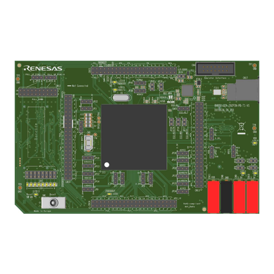
RH850/U2A 292pin 1. Overview Piggyback Board Views Following figures provide the top and bottom views of the piggyback board. Figure 1.1 Piggyback board top view Figure 1.2 Piggyback board bottom view R20UT4545ED0102 Rev.1.02 Page 8 of 58 May 27, 2021... - Page 9 RH850/U2A 292pin 1. Overview Following figures provide the drawing of top and bottom views of the piggyback board. VM O NO UT J P0_ AP4_ FLM D0 I C2- RXD2 G ND J P19 PULL_UP_PI N11- 19 PULL_UP_PI N1- 9...
-
Page 10: Mounting Of The Device
RH850/U2A 292pin 1. Overview Mounting of the Device The board is designed for use with the following devices: • R7F702300EABA (RH850/U2A16) • R7F702301EABG (RH850/U2A8) The device must be placed inside the socket IC1. To insert the device, align the device package A1 pin with the marking of the socket. -
Page 11: Jumpers, Connectors And Leds
RH850/U2A 292pin 2. Jumpers, Connectors and LEDs 2. Jumpers, Connectors and LEDs This section provides complete lists of all jumpers, connectors and LEDs. The placement of these components on the board is depicted in the figure below. Figure 2.1 Placement of jumpers, connectors and LEDs Figure 2.2 Placement of connectors on bottom side... - Page 12 Table 2.1 Jumpers overview (cont'd) Jumper Function Remark RHSIF I/F Rx/Tx signals swap refer to 6.6 Renesas High-Speed Serial I/F (RHSIF) / Multichannel Serial Peripheral • JP1[2-1]: RXDP/RXDN at pins 7 and 9 of CN5, Interface (MSPI) TXDP/TXDN at pins 1 and 3 of CN5 •...
- Page 13 RH850/U2A 292pin 2. Jumpers, Connectors and LEDs Table 2.1 Jumpers overview (cont'd) Jumper Function Remark JP13 Voltage selection for SVRAVCC refer to 3.2 Voltage Distribution • JP13[2-1]: 5.0 V • JP13[2-3]: 3.3 V JP14 Voltage selection for VDDIOF refer to 3.2 Voltage Distribution •...
- Page 14 RH850/U2A 292pin 2. Jumpers, Connectors and LEDs Table 2.1 Jumpers overview (cont'd) Jumper Function Remark JP31 Current measurement bridge of 3.3 V A/D refer to 3.4 Current Measurement Bridges Converter power supply JP32 Voltage selection for A0VCC refer to 3.2 Voltage Distribution •...
-
Page 15: Connectors Overview
Debug connector refer to 5 Debug and Flash Programming Interfaces and 7.2 Debug Connector CN4 RHSIF & MSPI connector refer to 6.6 Renesas High-Speed Serial I/F (RHSIF) / Multichannel Serial Peripheral Interface (MSPI) and 7.3 RHSIF/MSIP Connector CN5 Ethernet interface connector refer to 6.5 Automotive Ethernet Interface and... -
Page 16: Led Overview
RH850/U2A 292pin 2. Jumpers, Connectors and LEDs LED Overview The following table provides an overview of all LED. Table 2.3 LED overview Function Color Remark LED1 Device ERROROUT signal LED2 Signaling LED yellow connection via CN7, refer to 6.3 Signaling LEDs... -
Page 17: Power Supply
RH850/U2A 292pin 3. Power Supply 3. Power Supply Board Power Connection The device and the board require various power supply voltages: • 3.3 V for most of the digital circuitry on the device and on the board • 5 V in case some ports shall be operated with 5 V I/O voltage •... -
Page 18: Voltage Distribution
RH850/U2A 292pin 3. Power Supply Voltage Distribution The following table shows the required device power supply pins and their function: Table 3.1 Device power supply pins (cont'd) Device power supply pin Voltage Function E0VCC, E1VCC, E2VCC 3.3 V, 5 V... - Page 19 RH850/U2A 292pin 3. Power Supply Figure 3.1 Voltage distribution R20UT4545ED0102 Rev.1.02 Page 19 of 58 May 27, 2021...
-
Page 20: Device Core Voltage (Vdd) Selection
RH850/U2A 292pin 3. Power Supply Device Core Voltage (VDD) Selection The device core voltage VDD (typ.1.12 V) can be • supplied from external via CN11 (voltage IN_1v12) • generated from the P3V3 power rail by use of the on-board voltage regulator IC16 (voltage reg_vcc_VDD) •... -
Page 21: Power Supply Leds
RH850/U2A 292pin 3. Power Supply Power Supply LEDs The following green LEDs indicate the presence of various voltages on the piggyback board: • LED11 for 5.0 V power rail P5V0 • LED12 for 3.3 V power rail P3V3 • LED10 for 1.12 V device core voltage VDD R20UT4545ED0102 Rev.1.02... -
Page 22: Clock Supply
RH850/U2A 292pin 4. Clock Supply 4. Clock Supply The device's operation clock can be generated by • the on-chip oscillator main oscillator circuit in combination with an off-chip resonator, connected to the X1, X2 terminals • an off-chip oscillator, the clock is fed into the X1 terminal Figure 4.1 Clock supply... -
Page 23: Programmable Oscillator
RH850/U2A 292pin 4. Clock Supply Programmable Oscillator Instead of using the on-chip main oscillator a programmable crystal oscillator (OSC1) circuit can be soldered on the board. The available footprint and circuitry is designed for a SG-8002CE programmable crystal oscillator from Epson Toyocom. -
Page 24: Debug And Flash Programming Interfaces
For debugging and flash programming purposes debug and flash programming tools can be connected to the CN4 connector. Refer to 7.2 Debug Connector CN4 for details about the CN4 pin assignment. The Renesas standard emulator for RH850/U2A is the E2 emulator. This can be used as emulator for debugging or as flash programmer. R20UT4545ED0102 Rev.1.02... -
Page 25: Other Circuitry
RH850/U2A 292pin 6. Other Circuitry 6. Other Circuitry Operation Mode Selection The piggyback board gives the possibility to configure the following jumpers for selection of the device operation mode: Table 6.1 Device operation mode selection jumpers (cont'd) Jumper Function JP38 MODE0 pin level •... -
Page 26: Reset Switch
RH850/U2A 292pin 6. Other Circuitry RESET Switch The SW1 is used to issue a RESET to the device. The SW1 toggle switch allows to activate the RESET in two different ways: • SW1 in left '2-1(ON)' position: temporary reset Releasing the switch's lever returns the switch to its middle 'OFF' position and thus releases the reset. -
Page 27: Automotive Ethernet Interface
RH850/U2A 292pin 6. Other Circuitry • odd numbered pins 11, 13, 15, 17, 19 can be connected to − 5.0 V, if JP15[2-1] is set − 3.3 V, if JP15[2-3] is set Refer to 7.5 Pull-Up/Pull-Down Pin Header CN12 for CN12 details. - Page 28 RH850/U2A 292pin 6. Other Circuitry If a 2-wire connection should be used connector CN6 has to be assembled with the Würth block connector included in the delivery. In order to use CN6 it is necessary to populate the resistors R83 and R84 with 0 Ω resistors.
-
Page 29: Renesas High-Speed Serial I/F (Rhsif) / Multichannel Serial Peripheral Interface (Mspi)
RH850/U2A 292pin 6. Other Circuitry Renesas High-Speed Serial I/F (RHSIF) / Multichannel Serial Peripheral Interface (MSPI) The CN5 connector can be used to connect to the device's RHSIF and MSPI0 interface. Refer to 7.3 RHSIF/MSIP Connector CN5 for the CN5 pin assignment. -
Page 30: Connectors
RH850/U2A 292pin 7. Connectors 7. Connectors Connectors to the Main Board CN1 to CN3 Three connectors (CN1 to CN3) are available to connect the piggyback board to a Main Board. The signals of each connector are summarized in the following tables. - Page 31 RH850/U2A 292pin 7. Connectors Table 7.1 Main board connector CN1 (cont'd) Main Board function Piggyback board Main Board function Piggyback board device port device port ETH0RXD0 P10_3 ETH0TXD0 P20_9 ETH0RXD1 P10_4 ETH0TXD1 P20_10 ETH0RXD2 P10_5 ETH0TXD2 P20_12 ETH0RXD3 P10_6 ETH0TXD3...
-
Page 32: Main Board Connector Cn2
RH850/U2A 292pin 7. Connectors 7.1.2 Main Board Connector CN2 Table 7.2 Main board connector CN2 (cont'd) Function Device port Function Device port CAN2TX P3_2 CAN3TX P4_4 CAN2RX P3_3 CAN3RX P4_5 CAN4TX P4_6 CAN5TX P4_11 CAN4RX P4_7 CAN5RX P4_12 LIN2TX P2_0... -
Page 33: Main Board Connector Cn3
RH850/U2A 292pin 7. Connectors Table 7.2 Main board connector CN2 (cont'd) Function Device port Function Device port ‒ ‒ ‒ ‒ SFMA0CLK P17_5 SFMA0SSL P17_4 SFMA0IO0 P17_3 SFMA0IO1 P17_2 SFMA0IO2 P17_1 SFMA0IO3 P17_0 ‒ ‒ ‒ ‒ MMCA0CLK P24_4 MMCA0CMD... - Page 34 RH850/U2A 292pin 7. Connectors Table 7.3 Main board connector CN3 (cont'd) Function Device port Function Device port ‒ ‒ CSI1CS0 P24_7 ‒ ‒ DIGIO_24 P17_6 ‒ ‒ CSI1SO P24_6 CSI1SCLK P24_4 CSI1SI P24_5 ‒ ‒ ‒ ‒ ‒ ‒ ‒...
-
Page 35: Debug Connector Cn4
RH850/U2A 292pin 7. Connectors Table 7.3 Main board connector CN3 (cont'd) Function Device port Function Device port ‒ ‒ ‒ ‒ ‒ ‒ ‒ ‒ ‒ ‒ ‒ ‒ ‒ ‒ ‒ ‒ ‒ ‒ ‒ ‒ ‒ ‒ ‒... -
Page 36: Device Ports Connectors Cn13 To Cn16
RH850/U2A 292pin 7. Connectors Table 7.5 RHSIF/MISP connector CN5 cont'd JP1[2-1] JP1[2-3] Device port Function Device port Function P2_10 HSIF0_RXDN / MSPI0_SIN P2_12 HSIF0_TXDN / MSPI0_SON ‒ ‒ ‒ ‒ ‒ ‒ Note In order to minimize signal interference no signals from CN5 are connected to CN16. If required they can be connected via 0 Ω... -
Page 37: Device Ports Connector Cn13
RH850/U2A 292pin 7. Connectors 7.4.1 Device Ports Connector CN13 Device port Device port AP0_4 AP0_0 AP0_6 AP0_2 AP0_8 AP1_3 AP0_1 AP1_2 AP0_3 AP1_1 AP0_5 AP1_0 AP0_7 AP0_15 AP0_13 AP0_14 AP0_9 AP0_12 AP0_11 AP0_10 P3_3 P3_2 P24_5 P24_4 P24_6 P24_7 P24_8... -
Page 38: Device Ports Connector Cn14
RH850/U2A 292pin 7. Connectors 7.4.2 Device Ports Connector CN14 Table 7.6 Device ports connector CN14 Device port Device port P10_0 P10_1 P10_2 P10_3 P10_4 P10_5 P10_6 P10_7 P10_8 P10_9 P10_10 P10_11 P10_12 P10_13 P10_14 P21_6 P17_0 P21_7 P17_1 P17_2 P17_3... -
Page 39: Device Ports Connector Cn15
RH850/U2A 292pin 7. Connectors 7.4.3 Device Ports Connector CN15 Table 7.7 Device ports connector CN15 Device port Device port AP4_3 P4_15 AP4_2 P4_14 AP4_1 AP4_4 P6_11 AP4_0 P6_2 P6_4 P6_3 P6_6 P6_5 P6_8 P6_7 P6_12 P6_9 P6_10 P6_15 P6_14 P6_13... -
Page 40: Device Ports Connector Cn16
RH850/U2A 292pin 7. Connectors 7.4.4 Device Ports Connector CN16 Table 7.8 Device ports connector CN16 Device port Device port AWOVCL P2_1 P2_0 P2_3 P2_2 P2_5 P2_4 P2_7 P2_6 CN_P2_9 * P2_8 CN_P2_11 * CN_P2_10 * CN_P2_13 * CN_P2_12 * CN_P2_15 *... -
Page 41: Ethernet Connector Cn6 And Cn17
RH850/U2A 292pin 7. Connectors Ethernet Connector CN6 and CN17 Please refer to 6.5 Automotive Ethernet Interface for details on the function of these pins. Table 7.9 Ethernet connector CN6 Function MDIN_cn MDIP_cn Table 7.10 Ethernet connector CN17 Function MDIN_cn MDIP_cn GPIO/LED Connector CN20 Please refer to the data sheet of “Marvell 88Q2112 Automotive 100/1000BASE-T1 Transceiver”... -
Page 42: Jumper Configuration Examples
Due to the limited current capability of Renesas' E2 Emulator, powering the board only via this debugger is not feasible. In case of using another debug tool check its specification whether powering the piggyback board with the tool is possible. -
Page 43: Stand-Alone Operation With Single External Power Supply: Minimum Configuration
RH850/U2A 292pin 8. Jumper Configuration Examples 8.2.3 Stand-Alone Operation with Single External Power Supply: Minimum Configuration This example enables to operate the board with only the 3.3 V external power supply. Since no 5 V voltage is available, all I/O ports can only use 3.3 V. -
Page 44: Stand-Alone Operation With All External Power Supplies: Maximum Configuration
RH850/U2A 292pin 8. Jumper Configuration Examples 8.2.4 Stand-Alone Operation with All External Power Supplies: Maximum Configuration This example assumes all external power supplies are connected and used. • CN8: GND connection • CN9: 5 V − select desired 3.3 V/5.0 V via jumpers JP2, JP3, JP6 to JP14, JP22 and JP32 to JP3 Refer to 3.2Voltage Distribution for further details about VDD voltage and possible settings of jumpers JP2, JP3... -
Page 45: Operation On The Main Board: No External Supply
RH850/U2A 292pin 8. Jumper Configuration Examples 8.2.5 Operation on the Main Board: No External Supply This example assumes the piggyback board is plugged onto a Main Board, which provides 3.3 V and 5.0 V. Do not supply the 5V (CN9) and 3.3V (CN10) voltage directly to the piggyback board •... -
Page 46: Precautions
RH850/U2A 292pin 9. Precautions 9. Precautions Power-Off Sequence A dedicated sequence needs to be applied, when the power supply to the board is turned off. Please follow the below sequence: 1. At first turn the RESET switch SW1 into '2-3 ON' position, so that RESET is permanently asserted. -
Page 47: Mechanical Dimensions
RH850/U2A 292pin 10. Mechanical Dimensions 10. Mechanical Dimensions Figure 10.1 Mechanical dimensions R20UT4545ED0102 Rev.1.02 Page 47 of 58 May 27, 2021... -
Page 48: Schematics
RH850/U2A 292pin 11. Schematics 11. Schematics CAUTION The schematics shown in this document are not intended to be used as a reference for mass production. Any usage in an application design is in sole responsibility of the customer. The following components described in the schematics are not provided with the board upon delivery: •... - Page 49 RH850/U2A 292pin 11. Schematics 11.1 Page 1 R20UT4545ED0102 Rev.1.02 Page 49 of 58 May 27, 2021...
- Page 50 RH850/U2A 292pin 11. Schematics 11.2 Page 2 R20UT4545ED0102 Rev.1.02 Page 50 of 58 May 27, 2021...
- Page 51 RH850/U2A 292pin 11. Schematics 11.3 Page 3 R20UT4545ED0102 Rev.1.02 Page 51 of 58 May 27, 2021...
- Page 52 RH850/U2A 292pin 11. Schematics 11.4 Page 4 R20UT4545ED0102 Rev.1.02 Page 52 of 58 May 27, 2021...
- Page 53 RH850/U2A 292pin 11. Schematics 11.5 Page 5 R20UT4545ED0102 Rev.1.02 Page 53 of 58 May 27, 2021...
- Page 54 RH850/U2A 292pin 11. Schematics 11.6 Page 6 R20UT4545ED0102 Rev.1.02 Page 54 of 58 May 27, 2021...
- Page 55 Revision History Description Rev. Date Page Summary V1.02 2021-05-27 Added precaution for DeepSTOP mode in chapter 9.3 DeepSTOP Mode when using SVR ‒ V1.01 2019-10-29 Corrected document number in foot notes. ‒ V1.00 2019-06-14 Initial release...
- Page 56 Colophon RH850/U2A 292pin Piggyback Board V1 User's Manual: Piggyback Board Publication Date: Rev.1.02 May 27, 2021 Published by: Renesas Electronics Corporation...
- Page 57 Address List http://www.renesas.com SALES OFFICES Refer to "http://www.renesas.com/" for the latest and detailed information. Renesas Electronics America Inc. 1001 Murphy Ranch Road, Milpitas, CA 95035, U.S.A. Tel: +1-408-432-8888, Fax: +1-408-434-5351 Renesas Electronics Canada Limited 9251 Yonge Street, Suite 8309 Richmond Hill, Ontario Canada L4C 9T3...
- Page 58 Back Cover RH850/U2A 292pin R20UT4545ED0102...
Need help?
Do you have a question about the RH850/U2A 292pin and is the answer not in the manual?
Questions and answers