Renesas RH850 User Manual
Hide thumbs
Also See for RH850:
- Application note (45 pages) ,
- User manual (37 pages) ,
- User manual (17 pages)
Table of Contents
Advertisement
Cover
RH850 Evaluation Platform
RH850/U2A 292pin
32
Y-RH850-U2A-292PIN-PB-T1-V2
The newest version of this document can be obtained from the following web location:
Y-RH850-U2A-292PIN-PB-T1-V2 Documents
All information contained in these materials, including products and product specifications,
represents information on the product at the time of publication and is subject to change by
Renesas Electronics Corp. without notice. Please review the latest information published by
Renesas Electronics Corp. through various means, including the Renesas Electronics Corp.
website (https://www.renesas.com)
www.renesas.com
www.renesas.com
www.renesas.com
User's Manual: Piggyback Board
Rev.1.01 July 08, 2022
Advertisement
Table of Contents

Related Manuals for Renesas RH850


Summary of Contents for Renesas RH850
- Page 1 All information contained in these materials, including products and product specifications, represents information on the product at the time of publication and is subject to change by Renesas Electronics Corp. without notice. Please review the latest information published by Renesas Electronics Corp. through various means, including the Renesas Electronics Corp.
- Page 2 Renesas Electronics disclaims any and all liability for any damages or losses incurred by you or any third parties arising from the use of any Renesas Electronics product that is inconsistent with any Renesas Electronics data sheet, user’s manual or other Renesas Electronics document.
- Page 3 General Precautions in the Handling of Microprocessing Unit and Microcontroller Unit Products The following usage notes are applicable to all Microprocessing unit and Microcontroller unit products from Renesas. For detailed usage notes on the products covered by this document, refer to the relevant sections of the document as well as any technical updates that have been issued for the products.
-
Page 4: Table Of Contents
Signaling LEDs ............................ 30 Pull-Up/Pull-Down Pin Header ......................30 Automotive Ethernet Interface ......................31 Renesas High-Speed Serial I/F (RHSIF) / Multichannel Serial Peripheral Interface (MSPI) ....33 Connectors ........................ 34 Connectors to the Main Board CN1 to CN3 ..................34 7.1.1... - Page 5 RHSIF/MSIP Connector CN5 ......................42 Device Ports Connectors CN13 to CN16 .................... 43 7.4.1 Device Ports Connector CN13 ..................... 44 7.4.2 Device Ports Connector CN14 ..................... 45 7.4.3 Device Ports Connector CN15 ..................... 46 7.4.4 Device Ports Connector CN16 ..................... 47 Pull-Up/Pull-Down Pin Header CN12 ....................
-
Page 6: Overview
RENESAS MCU 1. Overview The RH850/U2A 292pin piggyback board is part of the RH850 Evaluation Platform and serves as a simple and easy to use platform for evaluating the features and performance of Renesas Electronics' 32-bit RH850/U2A 292pin microcontrollers. Notes 1. -
Page 7: Supported Main Boards
In the bag Note Please keep the Y-RH850-U2A-292PIN-PB-T1-V2 packing box at hand for later reuse in sending the product for repairs or for other purposes. Always use the original packing box when transporting the Y- RH850-U2A-292PIN-PB-T1-V2. If packing of your product is not complete, it may be damaged during transportation. -
Page 8: Piggyback Board Views
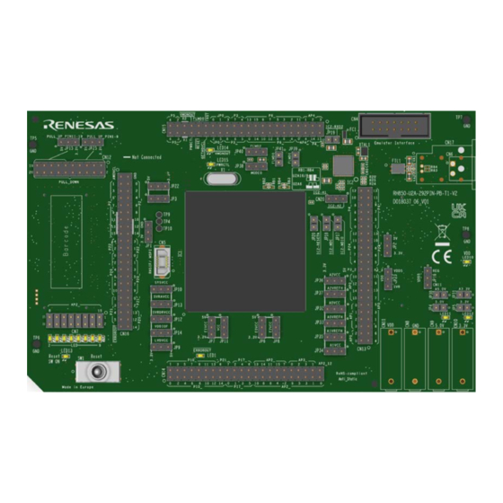
RH850/U2A 292pin 1. Overview Piggyback Board Views Following figures provide the top and bottom views of the piggyback board. Figure 1.1 Piggyback board top view Figure 1.2 Piggyback board bottom view R20UT4970ED0101 Rev.1.01 Page 8 of 67 July 08, 2022... - Page 9 RH850/U2A 292pin 1. Overview Following figures provide the drawing of top and bottom views of the piggyback board. Figure 1.3 PiggyBack Board top view Figure 1.4 PiggyBack Board bottom view R20UT4970ED0101 Rev.1.01 Page 9 of 67 July 08, 2022...
-
Page 10: Mounting Of The Device
R7F702301EABG-C (RH850/U2A8) • R7F702301AFABG-C (RH850/U2A8) • R7F702302FABB-C (RH850/U2A6) (NOTE: The board has to be modified in order to use • 1.6 Modifications for U2A6 device U2A6 device. Please see chapter The device must be placed inside the socket IC1. To insert the device, align the device package A1 pin with the marking of the socket. -
Page 11: Modifications For U2A6 Device
RH850/U2A 292pin 1. Overview Modifications for U2A6 device In order to use a U2A6 device with this piggyback board it is necessary to modify the board. Following connections must be changed: Device U2A16/8 U2A/6 Item to be modified Ball RX_DATA_P... -
Page 12: Difference From Y-Rh850-U2A-292Pin-Pb-T1-V1 To Y-Rh850-U2A-292Pin-Pb-T1-V2
1. Overview Difference from Y-RH850-U2A-292PIN-PB-T1-V1 to Y-RH850-U2A-292PIN-PB- T1-V2 Several changes have been applied to the new version of the 292pin RH850/U2A piggyback board compared to the first version. The table below summarizes all modifications. Table 1.2 Difference between Y-RH850-U2A-292PIN-PB-T1-V1 and Y-RH850-U2A-292PIN-PB-T1-V2... -
Page 13: Jumpers, Connectors And Leds
RH850/U2A 292pin 2. Jumpers, Connectors and LEDs 2. Jumpers, Connectors and LEDs This section provides complete lists of all jumpers, connectors and LEDs. The placement of these components on the board is depicted in the figure below. Figure 2.1 Placement of jumpers, connectors and LEDs Figure 2.2 Placement of connectors on bottom side... - Page 14 Table 2.1 Jumpers overview (cont'd) Jumper Function Remark RHSIF I/F Rx/Tx signals swap refer to 6.6 Renesas High-Speed Serial I/F (RHSIF) / Multichannel Serial Peripheral • JP1[2-1]: RXDP/RXDN at pins 7 and 9 of CN5, Interface (MSPI) TXDP/TXDN at pins 1 and 3 of CN5 •...
- Page 15 RH850/U2A 292pin 2. Jumpers, Connectors and LEDs Table 2.1 Jumpers overview (cont'd) Jumper Function Remark Voltage selection for LVDVCC refer to 3.2 Voltage Distribution • JP9[2-1]: 5.0 V • JP9[2-3]: 3.3 V JP10 Voltage selection for SYSVCC refer to 3.2 Voltage Distribution •...
- Page 16 RH850/U2A 292pin 2. Jumpers, Connectors and LEDs Table 2.1 Jumpers overview (cont'd) Jumper Function Remark JP18 Marvell MDC – U2A P3_6 • JP18[2-1]: Connected • JP18[OPEN]: Open JP19 Marvel RxD2 Pull down refer to 3.2 Voltage Distribution • JP19[2-1]: Connected •...
- Page 17 RH850/U2A 292pin 2. Jumpers, Connectors and LEDs Table 2.1 Jumpers overview (cont'd) Jumper Function Remark JP32 Voltage selection for A0VCC refer to 3.2 Voltage Distribution • JP32[2-1]: 5.0 V • JP32[2-3]: 3.3 V JP33 Voltage selection for A0VREFH refer to 3.2 Voltage Distribution •...
- Page 18 RH850/U2A 292pin 2. Jumpers, Connectors and LEDs Table 2.1 Jumpers overview (cont'd) Jumper Function Remark JP41 FLMD0 level selection refer to 6.1 Operation Mode Selection • JP41[2-1]: H level • JP41[OPEN]: − if no debug/programming tool connected: L level −...
-
Page 19: Connectors Overview
Debug connector refer to 5 Debug and Flash Programming Interfaces and 7.2 Debug Connector CN4 RHSIF & MSPI connector refer to 6.6 Renesas High-Speed Serial I/F (RHSIF) / Multichannel Serial Peripheral Interface (MSPI) and 7.3 RHSIF/MSIP Connector CN5 Ethernet interface connector refer to 6.5 Automotive Ethernet Interface and... -
Page 20: Led Overview
RH850/U2A 292pin 2. Jumpers, Connectors and LEDs LED Overview The following table provides an overview of all LED. Table 2.3 LED overview Function Color Remark LED1 Device ERROROUT signal LED2 Signaling LED yellow connection via CN7, refer to 6.3 Signaling LEDs... -
Page 21: Power Supply
RH850/U2A 292pin 3. Power Supply 3. Power Supply Board Power Connection The device and the board require various power supply voltages: • 3.3 V for most of the digital circuitry on the device and on the board • 5 V in case some ports shall be operated with 5 V I/O voltage •... -
Page 22: Voltage Distribution
RH850/U2A 292pin 3. Power Supply Voltage Distribution The following table shows the required device power supply pins and their function: Table 3.1 Device power supply pins (cont'd) Device power supply pin Voltage Function E0VCC, E1VCC, E2VCC 3.3 V, 5 V... - Page 23 RH850/U2A 292pin 3. Power Supply VOLTAGE DISTRIBUTION P3V3 P5V0 P3V3 P5V0 A5V0 A3V3 3.3V 5.0V 5.0V 3.3V 3.3V 5.0V 5.0V 3.3V JP30 JP31 E0VCC 3.3V or 5V A0VCC JP32 3.3V or 5V C104 E1VCC GETH0BVCC 3.3V or 5V A0VREFH 3.3V or 5V JP33 3.3V or 5V...
-
Page 24: Device Core Voltage (Vdd) Selection
RH850/U2A 292pin 3. Power Supply Device Core Voltage (VDD) Selection The device core voltage VDD (typ.1.12 V) can be • supplied from external via CN11 (voltage IN_1v12) • generated from the P3V3 power rail by use of the on-board voltage regulator IC16 (voltage reg_vcc_VDD) •... -
Page 25: Power Supply Leds
RH850/U2A 292pin 3. Power Supply Power Supply LEDs The following green LEDs indicate the presence of various voltages on the piggyback board: • LED11 for 5.0 V power rail P5V0 • LED12 for 3.3 V power rail P3V3 • LED10 for 1.12 V device core voltage VDD R20UT4970ED0101 Rev.1.01... -
Page 26: Clock Supply
RH850/U2A 292pin 4. Clock Supply 4. Clock Supply The device's operation clock can be generated by • the on-chip oscillator main oscillator circuit in combination with an off-chip resonator, connected to the X1, X2 terminals • an off-chip oscillator, the clock is fed into the X1 terminal P3V3 3.3V... -
Page 27: Programmable Oscillator
RH850/U2A 292pin 4. Clock Supply Programmable Oscillator Instead of using the on-chip main oscillator a programmable crystal oscillator (OSC1) circuit can be soldered on the board. The available footprint and circuitry is designed for a SG-8002CE programmable crystal oscillator from Epson Toyocom. The output of this oscillator can be connected to X1 terminal via resistor R2. -
Page 28: Debug And Flash Programming Interfaces
7.2 Debug Connector CN4 Refer to for details about the CN4 pin assignment. The Renesas standard emulator for RH850/U2A is the E2 emulator. This can be used as emulator for debugging or as flash programmer. R20UT4970ED0101 Rev.1.01 Page 28 of 67... -
Page 29: Other Circuitry
RH850/U2A 292pin 6. Other Circuitry 6. Other Circuitry Operation Mode Selection The piggyback board gives the possibility to configure the following jumpers for selection of the device operation mode: Table 6.1 Device operation mode selection jumpers (cont'd) Jumper Function JP38 MODE0 pin level •... -
Page 30: Reset Switch
RH850/U2A 292pin 6. Other Circuitry RESET Switch The SW1 is used to issue a RESET to the device. The SW1 toggle switch allows to activate the RESET in two different ways: • SW1 in left '2-1(ON)' position: temporary reset Releasing the switch's lever returns the switch to its middle 'OFF' position and thus releases the reset. -
Page 31: Automotive Ethernet Interface
RH850/U2A 292pin 6. Other Circuitry • odd numbered pins 1, 3, 5, 7, 9 can be connected to − 5.0 V, if JP25[2-1] is set − 3.3 V, if JP25[2-3] is set • odd numbered pins 11, 13, 15, 17, 19 can be connected to −... - Page 32 For an internal MOSC clock of 20MHz the crystal X1 has to be replaced by the 20MHz crystal included in the package. For package content please refer to Table 1.1 Package Components for the Y-RH850-U2A-292PIN- PB-T1-V2 2. The signals of the device's Fast Ethernet (R)MII interface (ETNB0) are available on the Main Board connectors.
-
Page 33: Renesas High-Speed Serial I/F (Rhsif) / Multichannel Serial Peripheral Interface (Mspi)
RH850/U2A 292pin 6. Other Circuitry Renesas High-Speed Serial I/F (RHSIF) / Multichannel Serial Peripheral Interface (MSPI) The CN5 connector can be used to connect to the device's RHSIF and MSPI0 interface. 7.3 RHSIF/MSIP Connector CN5 Refer to for the CN5 pin assignment. -
Page 34: Connectors
RH850/U2A 292pin 7. Connectors 7. Connectors Connectors to the Main Board CN1 to CN3 Three connectors (CN1 to CN3) are available to connect the piggyback board to a Main Board. The signals of each connector are summarized in the following tables. - Page 35 RH850/U2A 292pin 7. Connectors Table 7.1 Main board connector CN1 (cont'd) Main Board function Piggyback board Main Board function Piggyback board device port device port SENT0SPCO P24_6 SENT1SPCO P24_7 PSI5SRX0 P3_6 PSI5RX0 P5_4 PSI5STX0 P3_7 PSI5TX0 P5_6 ‒ ‒ PSI5SCLK0...
- Page 36 RH850/U2A 292pin 7. Connectors Table 7.1 Main board connector CN1 (cont'd) Main Board function Piggyback board Main Board function Piggyback board device port device port ‒ ‒ ‒ ‒ DIGIO_0 P21_2 DIGIO_1 P21_3 DIGIO_2 P21_4 DIGIO_3 P21_5 DIGIO_4 P21_6 DIGIO_5...
-
Page 37: Main Board Connector Cn2
RH850/U2A 292pin 7. Connectors 7.1.2 Main Board Connector CN2 Table 7.2 Main board connector CN2 (cont'd) Function Device port Function Device port CAN2TX P3_2 CAN3TX P4_4 CAN2RX P3_3 CAN3RX P4_5 CAN4TX P4_6 CAN5TX P4_11 CAN4RX P4_7 CAN5RX P4_12 LIN2TX P2_0... - Page 38 RH850/U2A 292pin 7. Connectors Table 7.2 Main board connector CN2 (cont'd) Function Device port Function Device port CAN6RX P4_15 CAN7RX P3_5 CAN8TX P10_6 CAN9TX P24_4 CAN8RX P10_5 CAN9RX P24_5 CAN10TX P24_6 CAN11TX P24_8 CAN10RX P24_7 CAN11RX P24_9 ‒ ‒ ‒...
-
Page 39: Main Board Connector Cn3
RH850/U2A 292pin 7. Connectors Table 7.2 Main board connector CN2 (cont'd) Function Device port Function Device port ‒ ‒ ETH1MDIO ETH1MDC ‒ ‒ ETH1RXD0 ETH1TXD0 ‒ ‒ ETH1RXD1 ETH1TXD1 ‒ ‒ ETH1RXD2 ETH1TXD2 ‒ ‒ ETH1RXD3 ETH1TXD3 ‒ ‒ ETH1RXCLK ETH1TXCLK ‒... - Page 40 RH850/U2A 292pin 7. Connectors Table 7.3 Main board connector CN3 (cont'd) Function Device port Function Device port CSI1CS2 P24_9 CSI1CS3 P4_8 ‒ ‒ CSI1CS0 P24_7 ‒ ‒ DIGIO_24 P17_6 ‒ ‒ CSI1SO P24_6 CSI1SCLK P24_4 CSI1SI P24_5 ‒ ‒ ‒...
- Page 41 RH850/U2A 292pin 7. Connectors Table 7.3 Main board connector CN3 (cont'd) Function Device port Function Device port DIGIO16 AP0_0 DIGIO17 AP0_1 DIGIO18 AP0_2 DIGIO19 AP0_3 DIGIO20 AP0_4 DIGIO21 AP0_5 DIGIO22 AP0_6 DIGIO23 AP0_7 ENC0 P10_8 ENC1 P10_9 ‒ ‒ ‒...
-
Page 42: Debug Connector Cn4
RH850/U2A 292pin 7. Connectors Debug Connector CN4 Table 7.4 On-chip debug connector CN4 Function Device port Function Device port TDCK / LPDCLK / JP0_2 FPCK TRSTZ FLMD0 ‒ TDO / LPDO / FPDT JP0_1 TDI / LPDIO / FPDR JP0_0 E0VCC ‒... -
Page 43: Device Ports Connectors Cn13 To Cn16
RH850/U2A 292pin 7. Connectors Note In order to minimize signal interference no signals from CN5 are connected to CN16. If required they can be connected via 0 Ω resistors R15 to R18 and R21 to R23. Device Ports Connectors CN13 to CN16 The device port connectors enable easy connection to almost all ports of the device. -
Page 44: Device Ports Connector Cn13
RH850/U2A 292pin 7. Connectors 7.4.1 Device Ports Connector CN13 Device port Device port AP0_4 AP0_0 AP0_6 AP0_2 AP0_8 AP1_3 AP0_1 AP1_2 AP0_3 AP1_1 AP0_5 AP1_0 AP0_7 AP0_15 AP0_13 AP0_14 AP0_9 AP0_12 AP0_11 AP0_10 P3_3 P3_2 P24_5 P24_4 P24_6 P24_7 P24_8... -
Page 45: Device Ports Connector Cn14
RH850/U2A 292pin 7. Connectors 7.4.2 Device Ports Connector CN14 Table 7.6 Device ports connector CN14 Device port Device port P10_0 P10_1 P10_2 P10_3 P10_4 P10_5 P10_6 P10_7 P10_8 P10_9 P10_10 P10_11 P10_12 P10_13 P10_14 P21_6 P17_0 P21_7 P17_1 P17_2 P17_3... -
Page 46: Device Ports Connector Cn15
RH850/U2A 292pin 7. Connectors 7.4.3 Device Ports Connector CN15 Table 7.7 Device ports connector CN15 Device port Device port AP4_3 P4_15 AP4_2 P4_14 AP4_1 AP4_4 P6_11 AP4_0 P6_2 P6_4 P6_3 P6_6 P6_5 P6_8 P6_7 P6_12 P6_9 P6_10 P6_15 P6_14 P6_13... -
Page 47: Device Ports Connector Cn16
RH850/U2A 292pin 7. Connectors 7.4.4 Device Ports Connector CN16 Table 7.8 Device ports connector CN16 Device port Device port AWOVCL P2_1 P2_0 P2_3 P2_2 P2_5 P2_4 P2_7 P2_6 CN_P2_9 * P2_8 CN_P2_11 * CN_P2_10 * CN_P2_13 * CN_P2_12 * CN_P2_15 *... -
Page 48: Pull-Up/Pull-Down Pin Header Cn12
RH850/U2A 292pin 7. Connectors Pull-Up/Pull-Down Pin Header CN12 Function Function fixed H level, depends on JP25: fixed L level • JP25[2-1]: 5.0 V • JP25[2-3]: 3.3 V fixed H level, depends on JP15: • JP15[2-1]: 5.0 V • JP15[2-3]: 3.3 V Ethernet Connector CN6 and CN17 6.5 Automotive Ethernet Interface... -
Page 49: Gpio/Led Connector Cn20
RH850/U2A 292pin 7. Connectors GPIO/LED Connector CN20 Please refer to the data sheet of “Marvell 88Q2112 Automotive 100/1000BASE-T1 Transceiver” for details on the function of these pins. Table 7.11 GPIO/LED connector CN20 JP1[2-1] Device port Function GPIO, pin 42 GPIO output of Marvell PHY... -
Page 50: Jumper Configuration Examples
Due to the limited current capability of Renesas' E2 Emulator, powering the board only via this debugger is not feasible. -
Page 51: Configuration Examples
RH850/U2A 292pin 8. Jumper Configuration Examples Configuration Examples 8.2.1 General Settings All of the following board configurations are based on these conditions: • Normal device operation mode (JP41[OPEN]: FLMD0 = L). • All voltages for all functions are activated. •... -
Page 52: Stand-Alone Operation With Single External Power Supply: Minimum Configuration
RH850/U2A 292pin 8. Jumper Configuration Examples 8.2.3 Stand-Alone Operation with Single External Power Supply: Minimum Configuration This example enables to operate the board with only the 3.3 V external power supply. Since no 5 V voltage is available, all I/O ports can only use 3.3 V. -
Page 53: Stand-Alone Operation With All External Power Supplies: Maximum Configuration
RH850/U2A 292pin 8. Jumper Configuration Examples 8.2.4 Stand-Alone Operation with All External Power Supplies: Maximum Configuration This example assumes all external power supplies are connected and used. • CN8: GND connection • CN9: 5 V − select desired 3.3 V/5.0 V via jumpers JP2, JP3, JP6 to JP14, JP22 and JP32 to JP3 Refer to 3.2Voltage Distribution for further details about VDD voltage and possible settings of jumpers JP2, JP3... -
Page 54: Operation On The Main Board: No External Supply
RH850/U2A 292pin 8. Jumper Configuration Examples 8.2.5 Operation on the Main Board: No External Supply This example assumes the piggyback board is plugged onto a Main Board, which provides 3.3 V and 5.0 V. Do not supply the 5V (CN9) and 3.3V (CN10) voltage directly to the piggyback board •... -
Page 55: Precautions
RH850/U2A 292pin 9. Precautions 9. Precautions Power-Off Sequence A dedicated sequence needs to be applied, when the power supply to the board is turned off. Please follow the below sequence: 1. At first turn the RESET switch SW1 into '2-3 ON' position, so that RESET is permanently asserted. -
Page 56: Mechanical Dimensions
RH850/U2A 292pin 10. Mechanical Dimensions 10. Mechanical Dimensions Figure 9.1 Mechanical dimensions R20UT4970ED0101 Rev.1.01 Page 56 of 67 July 08, 2022... -
Page 57: Schematics
RH850/U2A 292pin 11. Schematics 11. Schematics CAUTION The schematics shown in this document are not intended to be used as a reference for mass production. Any usage in an application design is in sole responsibility of the customer. The following components described in the schematics are not provided with the board upon delivery: •... - Page 58 RH850/U2A 292pin 11. Schematics 11.1 Page 1 R20UT4970ED0101 Rev.1.01 Page 58 of 67 July 08, 2022...
- Page 59 RH850/U2A 292pin 11. Schematics 11.2 Page 2 R20UT4970ED0101 Rev.1.01 Page 59 of 67 July 08, 2022...
- Page 60 RH850/U2A 292pin 11. Schematics 11.3 Page 3 R20UT4970ED0101 Rev.1.01 Page 60 of 67 July 08, 2022...
- Page 61 RH850/U2A 292pin 11. Schematics 11.4 Page 4 R20UT4970ED0101 Rev.1.01 Page 61 of 67 July 08, 2022...
- Page 62 RH850/U2A 292pin 11. Schematics 11.5 Page 5 R20UT4970ED0101 Rev.1.01 Page 62 of 67 July 08, 2022...
- Page 63 RH850/U2A 292pin 11. Schematics 11.6 Page 6 R20UT4970ED0101 Rev.1.01 Page 63 of 67 July 08, 2022...
- Page 64 Revision History Description Rev. Date Page Summary V1.01 2022-07-08 52 - 54 Corrected jumper JP41 setting in Figure 8.1 Stand-alone operation with minimum external power supply, Figure 8.2 Stand-alone operation with maximum external power supply and Figure 8.3 Main board operation without external power supply. ‒...
- Page 65 Colophon RH850/U2A 292pin Piggyback Board V2 User's Manual: Piggyback Board Publication Date: Rev.1.01 July 08, 2022 Published by: Renesas Electronics Corporation...
- Page 66 Address List http://www.renesas.com SALES OFFICES Refer to "http://www.renesas.com/" for the latest and detailed information. Renesas Electronics America Inc. 1001 Murphy Ranch Road, Milpitas, CA 95035, U.S.A. Tel: +1-408-432-8888, Fax: +1-408-434-5351 Renesas Electronics Canada Limited 9251 Yonge Street, Suite 8309 Richmond Hill, Ontario Canada L4C 9T3...
- Page 67 Back Cover RH850/U2A 292pin R20UT4970ED0101...
Need help?
Do you have a question about the RH850 and is the answer not in the manual?
Questions and answers