Table of Contents
Advertisement
Quick Links
All manuals and user guides at all-guides.com
UM2174
User manual
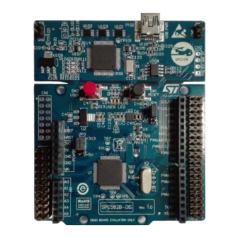
SPC582B-DIS Discovery Board
Introduction
The SPC582B-DIS is a low-cost development board to evaluate and develop applications
with the microcontroller SPC582B60E1 in eTQFP 64-pin package.
This document describes the hardware architecture of the SPC582B-DIS Discovery board
and in which way the jumpers can be set to enable specific functions.
June 2020
UM2174 Rev 3
1/23
1
www.st.com
Advertisement
Table of Contents

Related Manuals for ST SPC582B-DIS


Summary of Contents for ST SPC582B-DIS
- Page 1 User manual SPC582B-DIS Discovery Board Introduction The SPC582B-DIS is a low-cost development board to evaluate and develop applications with the microcontroller SPC582B60E1 in eTQFP 64-pin package. This document describes the hardware architecture of the SPC582B-DIS Discovery board and in which way the jumpers can be set to enable specific functions.
-
Page 2: Table Of Contents
SPC582B-DIS Discovery board with SPC582B60E1 ....5 SPC582B-DIS Discovery board ....... . . 5 Hardware overview . - Page 3 All manuals and user guides at all-guides.com UM2174 List of tables List of tables Table 1. Power source and jumpers configuration ........7 Table 2.
- Page 4 SPC582B-DIS ........
-
Page 5: Spc582B-Dis Discovery Board With Spc582B60E1
CPU 80MHz, 1088 KB (1024 KB code flash + 64 KB data flash) 96 KB SRAM in an eTQFP64 package. The SPC582B-DIS allows full access to peripherals such as DSPI, LINFlexD, ISO CAN-FD. The new features satisfy the ASIL-B requirements. - Page 6 UM2174 All CPUs pins are connected to two-pin arrays; this solution simplifies the debug activity as well as it reduces the effort to connect the SPC582B-DIS to the final user application board. A standard 2x7pin JTAG port is available to program and debug the microcontroller by using third part tools.
-
Page 7: Hardware Overview
UM2174 Hardware overview Hardware overview Power supply section SPC582B-DIS can be supplied by using some DC sources, setting some jumpers properly: by the host PC through the USB cable (+5 V; this is the default configuration); by an external source connected to VIN pin (CN6 pin 8, CN7 pin 8) (7÷12V ... -
Page 8: Figure 2. Usb Port - 5 V Input
All manuals and user guides at all-guides.com Hardware overview UM2174 Figure 2. USB Port - 5 V input Figure 3. +5 V regulator (external PSU) and 5 V selector (SB17-SB27) Figure 4. +3.3 V voltage regulator and +3.3 V selector (SB26) 8/23 UM2174 Rev 3... -
Page 9: Microcontroller Power Management
UDE PLS software. The debugger serial number is reported on the label applied on the board (bottom side). The integrated debugger SW is accessible via ST's free integrated development environment, SPC5Studio (www.st.com/spc5studio). To download the debugger software and to activate license refer to the PLS website. -
Page 10: Table 2. Programmer/Debugger - Jumpers Setting
All manuals and user guides at all-guides.com Hardware overview UM2174 (Tx), pin 39 (Rx) and two level shifters implement this feature.Table 2 shows how to set the jumpers. Note: The board comes with the integrated programmer enabled. Table 2. Programmer/Debugger - Jumpers setting SB23 SB10 SB11... -
Page 11: Crystal Oscillator
All manuals and user guides at all-guides.com UM2174 Hardware overview Figure 8. PLS Integrated Programmer/Debugger (part II - Level shifters and EEPROM) Figure 9. PLS Integrated Programmer/Debugger (part III - Jumper configuration) Crystal oscillator The board accepts different clock sources. In the default HW configuration a 40MHz crystal (X2) is connected to the microcontroller oscillator pins. -
Page 12: Reset Circuit
External reset circuit Open Close User LEDs, User Button In the SPC582B-DIS board three LEDs are available for user purposes; see 12. The Figure jumpers SB18, SB19 and SB20 allow disconnecting the anode of each LED and then let the user to reserve these pins for a different purpose. -
Page 13: Connectors
All manuals and user guides at all-guides.com UM2174 Hardware overview Figure 12. User LEDs The pushbutton SW2 is reserved for user purpose (see 13). If the jumper SB21 is left Figure open, PF2 port is available for a different purpose. Figure 13. -
Page 14: Table 6. Cn8 - Arduino Uno-R3 Analog Input
All manuals and user guides at all-guides.com Hardware overview UM2174 Table 5. CN6 - Arduino UNO-R3 Power (continued) Connector CN6 Arduino UnoR3 Power CN6 Pin Function / Signal Table 6. CN8 - Arduino UNO-R3 Analog Input Connector CN8 Arduino UnoR3 Alternate Alternate Analog In... -
Page 15: Extended Connectors (I/O Headers)
All manuals and user guides at all-guides.com UM2174 Hardware overview Table 8. CN9 - Arduino UNO-R3 Digital PWM (D7÷D0) Arduino UnoR3 uC uC Alternate Alternate Alternate Digital PWM CN9 Pin Function Function Function Function (part2) Port LINFlex1 LINFlex1 LINFlex2 UC11 INT19 LINFlex2 UC10... -
Page 16: Table 10. Cn10 - Extended Connectors (I/O Headers)
All manuals and user guides at all-guides.com Hardware overview UM2174 Table 9. CN7 - Extended Connectors (I/O Headers) (continued) Connector CN7 Alternate Alternate Signal Function Function Function Port VDD_HV_IO AVDD A0 (CN8) Ext Clock SIN - A1 (CN8) PD12 AN[15] UC14 DSPI_3 E3V3... - Page 17 All manuals and user guides at all-guides.com UM2174 Hardware overview Table 10. CN10 - Extended Connectors (I/O Headers) (continued) Connector CN10 Alternate Alternate Alternate Signal CN10 Function Function Function Function Port AVDD (CN5) SCK - D13 (CN5) PG11 UC19 AN[57] DSPI_0 LINFlexD1 5 RXD...
- Page 18 All manuals and user guides at all-guides.com Hardware overview UM2174 Table 10. CN10 - Extended Connectors (I/O Headers) (continued) Connector CN10 Alternate Alternate Alternate Signal CN10 Function Function Function Function Port SIN - M_CAN_1 D4 (CN9) PC13 UC28 DSPI_1 SCK - UC22 REQ4 DSPI_2...
-
Page 19: Bt Module Connector
All manuals and user guides at all-guides.com UM2174 Hardware overview 2.7.3 BT Module Connector Table 11. CN2 - BT Module Connector CN2 Connector Signal Alternate Function Port Function (1) LINFlexD15 TXD LINFlexD15 RXD 2.7.4 JTAG Connector Table 12. CN1 - JTAG Connector CN1 Connector CN1 Pin Function... -
Page 20: Appendix A Board Layout
All manuals and user guides at all-guides.com Board layout UM2174 Appendix A Board layout PCB layout Figure 14. PCB Layout - Top Side 20/23 UM2174 Rev 3... -
Page 21: Figure 15. Pcb Layout - Bottom Side
All manuals and user guides at all-guides.com UM2174 Board layout Figure 15. PCB Layout - Bottom Side UM2174 Rev 3 21/23... -
Page 22: Revision History
All manuals and user guides at all-guides.com Revision history UM2174 Revision history Table 13. Document revision history Date Revision Changes 15-Mar-2017 Initial release. 20-Jun-2017 Updated Section : Introduction. 04-Jun-2020 UpdatedTable 7 22/23 UM2174 Rev 3... - Page 23 ST products and/or to this document at any time without notice. Purchasers should obtain the latest relevant information on ST products before placing orders. ST products are sold pursuant to ST’s terms and conditions of sale in place at the time of order acknowledgement.
Need help?
Do you have a question about the SPC582B-DIS and is the answer not in the manual?
Questions and answers