Fuji Electric P642 Series Applications Manual
Small ipm intelligent power module
Hide thumbs
Also See for P642 Series:
- Mounting instruction (14 pages) ,
- Applications manual (13 pages)

Related Manuals for Fuji Electric P642 Series


Summary of Contents for Fuji Electric P642 Series
- Page 1 Small IPM (Intelligent Power Module) P642 Series 6MBP**XT*065-50 Application Manual April 2024 MT6M15234 c © Fuji Electric Co., Ltd. All rights reserved.
- Page 2 Fuji Electric Co., Ltd. If you have any question about any portion of this application note, ask Fuji Electric Co., Ltd. or its sales agencies. Neither Fuji Electric Co., Ltd. nor its agencies shall be liable for any injury or damage caused by any use of the products not in accordance with instructions set forth herein.
-
Page 3: Table Of Contents
2. Short Circuit Protection 3. Setting of External Shunt Resistor for Overcurrent Protection Chapter 5 Recommended Wiring and Layout 1. Examples of Application Circuit 2. Recommendations and Precautions in PCB Design MT6M15234 c © Fuji Electric Co., Ltd. All rights reserved. - Page 4 Mounting Guidelines and Thermal Design 1. Soldering to PCB 2. Mounting to Heat Sink 3. Heat Sink Selection Chapter 7 Notes 1. Precautions for Use 2. Precautions for Handling and Storage MT6M15234 c © Fuji Electric Co., Ltd. All rights reserved.
-
Page 5: Product Outline
Chapter 1 Product Outline 1. Introduction 2. Product Lineup and Target Application 3. Definition of Type Name 4. Marking Specification 5. Package Outline Dimensions 6. Absolute Maximum Ratings MT6M15234 c © Fuji Electric Co., Ltd. All rights reserved. -
Page 6: Introduction
IGBT is short and the impedance of the drive circuit is low. • IPM has built-in bootstrap diodes (BSD) and can be driven by a single power supply. No insulated power supplies for the high-side drive are needed. MT6M15234 c © Fuji Electric Co., Ltd. All rights reserved. - Page 7 Fig.1-1 Internal circuit diagram MT6M15234 c © Fuji Electric Co., Ltd. All rights reserved.
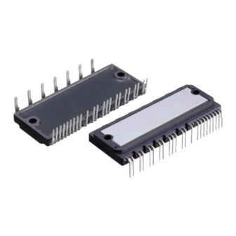
- Page 8 • This product uses aluminum insulated metal substrate (IMS) and has excellent heat dissipation. • The pitch between control terminals is 2.54mm. • The pitch between power terminals is 10mm. Fig.1-2 Package external view MT6M15234 c © Fuji Electric Co., Ltd. All rights reserved.
-
Page 9: Product Lineup And Target Application
Type Name Isolation Voltage [Vrms] Variation Voltage Current 6MBP50XTA065-50 6MBP50XTC065-50 2500Vrms Sinusoidal 60Hz, 1min. (Between all shorted terminals and IMS) 6MBP75XTA065-50 6MBP75XTC065-50 (LT): Temperature sensor output function (OH): Overheating protection function MT6M15234 c © Fuji Electric Co., Ltd. All rights reserved. -
Page 10: Definition Of Type Name
Series name T: Package type Series name X: Chip generation IGBT current rating 50:50A, 75:75A Indicates IGBT-IPM Number of switching elements 6 : 6 switching elements Fig. 1-3 Definition of Type MT6M15234 c © Fuji Electric Co., Ltd. All rights reserved. -
Page 11: Marking Specification
4. Marking Specification Fig. 1-4 Marking specification Table 1-2 Products code PRODUCT CODE TYPE NAME 6MBP50XTA065-50 6MBP50XTC065-50 6MBP75XTA065-50 6MBP75XTC065-50 MT6M15234 c © Fuji Electric Co., Ltd. All rights reserved. - Page 12 The IMS (Insulated Metal Substrate) is deliberately protruded to improve the thermal conductivity between IMS and heat-sink. Note.2 Thickness from the package surface to the back side including the IMS. Fig. 1-5 Case outline drawing MT6M15234 c © Fuji Electric Co., Ltd. All rights reserved.
-
Page 13: Absolute Maximum Ratings
The maximum virtual junction temperature during continuous operation is T =150 Continuous operation at over T =150 C may result in degradation of product lifetime such as power cycling capability with respect to the designed lifetime. MT6M15234 c © Fuji Electric Co., Ltd. All rights reserved. - Page 14 Fault Signal Current terminals. (Continued on next page.) Apply 13.0V or more between VB(U)-U, VB(V)-V, VB(W)-W terminals. The product might malfunction if the high-side bias offset voltage is less than -5V. 1-10 MT6M15234 c © Fuji Electric Co., Ltd. All rights reserved.
- Page 15 CFO is output terminal. Do not apply voltage or current. Connect only the specified capacitor between CFO-COM terminals. VSC is output terminal. Do not apply voltage or current. Connect only the specified resistor between VSC-COM terminals. 1-11 MT6M15234 c © Fuji Electric Co., Ltd. All rights reserved.
- Page 16 DC(Surge,terminal) P-N(U, V, W) DC(Surge,terminal) DC(sc) CE(chip) 短絡電流 (b) During FWD reverse recovery (c) During short-circuit Fig.1-6 Waveforms and Collector-Emitter voltage during IGBT turn-off, FWD reverse recovery, and short-circuit 1-12 MT6M15234 c © Fuji Electric Co., Ltd. All rights reserved.
-
Page 17: Chapter 2 Description Of Terminal Symbols And Terminology
Chapter 2 Description of Terminal Symbols and Terminology 1. Description of Terminal Symbols 2. Description of Terminology MT6M15234 c © Fuji Electric Co., Ltd. All rights reserved. -
Page 18: Description Of Terminal Symbols
High-side Bias Voltage for VB(W) W-phase Output W-phase High-side Bias Voltage for VS(W) V-phase Output W-phase GND Low-side Sense Current U-phase Output Detection Low-side Control Power VCCL Positive Bus Voltage Input Supply MT6M15234 c © Fuji Electric Co., Ltd. All rights reserved. -
Page 19: Description Of Terminology
Bootstrap circuit VB(W)-VS(W) (for each phase). Input signal threshold voltage that turns on the IGBT. Input Signal Threshold th(on) Voltage Input signal threshold voltage that turns off the IGBT. th(off) MT6M15234 c © Fuji Electric Co., Ltd. All rights reserved. - Page 20 V CCL(hys) CCL(OFF) CCL(ON) Hysteresis of Low-side If the pulse width of the input signal is less than t or t , the product might make incorrect IN(on) IN(off) response. MT6M15234 c © Fuji Electric Co., Ltd. All rights reserved.
- Page 21 Flatness of the IMS’s aluminum surface. Refer to Fig. 2-4. Flatness Weight Weight of a single IPM. Resistance to Soldering Number of times of solder heat resistance under specified Heat conditions. MT6M15234 c © Fuji Electric Co., Ltd. All rights reserved.
- Page 22 Fig. 2-2 Definition of switching time Temperature sensor position Approx. 21.6 Approx. 8.3 Heat sink side measurement position Unit:mm SIDE VIEW TOP VIEW Fig. 2-3 Temperature sensor position and T measurement position MT6M15234 c © Fuji Electric Co., Ltd. All rights reserved.
- Page 23 (A2) (A1) Fig. 2-4 Measurement point of heat sink surface flatness MT6M15234 c © Fuji Electric Co., Ltd. All rights reserved.
-
Page 24: Details Of Control & Protection Functions
4. Signal Input, IN(HU,HV,HW), IN(LU,LV,LW) 3-14 5. Overcurrent Protection Function, IS 3-17 6. Fault Status Output Function, VFO, CFO 3-19 7. Temperature Output Function, TEMP 3-21 8. Overheating Protection Function 3-23 MT6M15234 c © Fuji Electric Co., Ltd. All rights reserved. -
Page 25: Control Power Supply, Vcch(U,V,W), Vccl, Com
Control circuit in the product might be damaged. It is recommended to Over 20 insert a Zener diode between each pair of control supply terminals if necessary. *1:V is applied between VB(U)-U, VB(V)-V, VB(W)-W. B(*) MT6M15234 c © Fuji Electric Co., Ltd. All rights reserved. - Page 26 The diode is connected to protect the product from the input surge voltage. Do not use the diode for voltage clamp purpose otherwise the product might be damaged. Fig. 3-1 UV protection circuit of high-side and low-side control power supply MT6M15234 c © Fuji Electric Co., Ltd. All rights reserved.
- Page 27 <4> When the voltage drop time is more than t , the fault output pulse width is generated and all lower side IGBTs are OFF state regardless of the input signal condition during the same time. MT6M15234 c © Fuji Electric Co., Ltd. All rights reserved.
- Page 28 VFO keeps high level. <3> The HVIC starts to operate from the next input signal after UV is reset. : The fault output does not depend on the bias condition of the HVIC. MT6M15234 c © Fuji Electric Co., Ltd. All rights reserved.
- Page 29 Control circuit in the product might be damaged. It is recommended Over 20 to insert a Zener diode between each pair of high-side power supply terminals. MT6M15234 c © Fuji Electric Co., Ltd. All rights reserved.
- Page 30 These diodes protect the product from input surge voltage. Do not use these diodes for voltage clamp purpose otherwise the product might be damaged. Fig. 3-4 UV protection circuit of high-side bias voltage MT6M15234 c © Fuji Electric Co., Ltd. All rights reserved.
- Page 31 <3> After UV protection is reset, HVIC restarts switching operation from the next input signal. *1 : The fault output does not depend on the bias condition of the HVIC. MT6M15234 c © Fuji Electric Co., Ltd. All rights reserved.
-
Page 32: Function Of Built-In Bsds (Bootstrap Diodes)
(t1) by high-side control power supply. High-side bias voltage V B(*) C natural discharge Fig. 3-7 Timing chart of charging operation when low-side IGBT is ON MT6M15234 c © Fuji Electric Co., Ltd. All rights reserved. - Page 33 (FWD:ON) (t2) High-side bias voltage V B(*) decreases due to current consumption by high-side control power supply. Fig. 3-9 Timing chart of charging operation when low-side FWD is ON 3-10 MT6M15234 c © Fuji Electric Co., Ltd. All rights reserved.
- Page 34 Gate signal of low-side IGBT High-side bias voltage V B(*) decreases due to current consumption by high-side control power supply. Fig. 3-10 Timing chart of charging and discharging operation 3-11 MT6M15234 c © Fuji Electric Co., Ltd. All rights reserved.
- Page 35 Low-side, high-side control power supply voltage V start High-side bias voltage V B(*) Gate signal of low-side IGBT Initial charging period Fig. 3-12 Timing chart of initial charging operation 3-12 MT6M15234 c © Fuji Electric Co., Ltd. All rights reserved.
- Page 36 The bootstrap diode has built-in current limiting resistor of 20Ω (typ.). Fig. 3-13 and Fig. 3-14 show the characteristics of the bootstrap diode. Fig. 3-13 V characteristic of BSD Fig. 3-14 V characteristic of BSD (zoom at low current range) 3-13 MT6M15234 c © Fuji Electric Co., Ltd. All rights reserved.
-
Page 37: Signal Input, In(Hu,Hv,Hw), In(Lu,Lv,Lw)
Adjust the RC constant according to the PWM control method and the wiring pattern of the printed circuit board. IN(HU), IN(HV), IN(HW) IN(LU), IN(LV), IN(LW) Fig. 3-15 Recommended MPU I/O interface circuit of IN(HU,HV,HW), IN(LU,LV,LW) terminals 3-14 MT6M15234 c © Fuji Electric Co., Ltd. All rights reserved. - Page 38 IN(HU,HV,HW,LU,LV,LW)-COM terminals. These diodes are built-in to protect the product from input surge voltage. Do not use these diodes for voltage clamp purpose as it might damage the product. Fig.3-16 Circuit of IN(HU,HV,HW), IN(LU,LV,LW) terminals 3-15 MT6M15234 c © Fuji Electric Co., Ltd. All rights reserved.
- Page 39 Fig. 3-17 IGBT drive state versus input signal ON pulse width Outside recommended Recommended range range IN(off) minimum Fig. 3-18 IGBT drive state versus input signal OFF pulse width 3-16 MT6M15234 c © Fuji Electric Co., Ltd. All rights reserved.
-
Page 40: Overcurrent Protection Function, Is
Do not use these diodes for voltage clamp purpose as it might damage the product. Fig. 3-19 OC protection detection circuit of IS terminal 3-17 MT6M15234 c © Fuji Electric Co., Ltd. All rights reserved. - Page 41 . Propagation delay of LVIC is included in t d(IS) d(IS) t4: OC protection is reset after t . LVIC restarts switching operation from the next input signal. 3-18 MT6M15234 c © Fuji Electric Co., Ltd. All rights reserved.
-
Page 42: Fault Status Output Function, Vfo, Cfo
• Fig. 3-22 shows the voltage-current characteristics of VFO terminal during fault status output. I the sink current of VFO terminal. Fig. 3-21 Recommended MPU I/O interface circuit of VFO terminal 3-19 MT6M15234 c © Fuji Electric Co., Ltd. All rights reserved. - Page 43 0.16 0.14 0.12 0.10 0.08 0.06 0.04 10kΩ resistance to 5V pull-up 0.02 0.00 [mA] Fig. 3-22 Voltage-current characteristics of VFO terminal during fault status output 3-20 MT6M15234 c © Fuji Electric Co., Ltd. All rights reserved.
-
Page 44: Temperature Output Function, Temp
5kΩ pull-down resistor. • Fig. 3-26 shows the operation sequence of the TEMP terminal during startup and shutdown of product. Fig. 3-23 Recommended MPU I/O interface circuit of TEMP terminal 3-21 MT6M15234 c © Fuji Electric Co., Ltd. All rights reserved. - Page 45 V exceeds V CCL (ON) t3-t4 : TEMP output function is reset when V falls below V . TEMP output voltage is the same CCL(OFF) as clamp voltage. 3-22 MT6M15234 c © Fuji Electric Co., Ltd. All rights reserved.
-
Page 46: Overheating Protection Function
<4> : Fault status and OH protection status are reset after LVIC virtual junction temperature falls below T and t has elapsed. The low-side IGBTs restart operation from the next OH(hys) input signal. T is the hysteresis temperature of overheating protection. OH(hys) 3-23 MT6M15234 c © Fuji Electric Co., Ltd. All rights reserved. -
Page 47: Details Of Inverter Block
Chapter 4 Details of Inverter Block 1. Connection of Bus Voltage Input Terminal and Low-side IGBTs Emitter 2. Short Circuit Protection 3. Setting of External Shunt Resistor for Overcurrent Protection MT6M15234 c © Fuji Electric Co., Ltd. All rights reserved. -
Page 48: Connection Of Bus Voltage Input Terminal And Low-Side Igbts Emitter
"B" is greater than that at location "A" or "C", location "C" is recommended considering the impact to the current detection accuracy. • Snubber capacity of 0.1 ~ 0.22 μF is recommended. MT6M15234 c © Fuji Electric Co., Ltd. All rights reserved. -
Page 49: Short Circuit Protection
* When using the external shunt resistor method, connect the VSC terminal to the control GND with the specified sense resistor instead of leaving it open. Sense current method External shunt resistor method Fig. 4-2 SC detection circuits MT6M15234 c © Fuji Electric Co., Ltd. All rights reserved. - Page 50 =40.2Ω) Table 4-3 SC protection current value with shunt resistors (6MBP50XTA065-50, R External shunt resistance OC protection current (Min.) None 85 A 3 mΩ 57 A 5 mΩ 48 A MT6M15234 c © Fuji Electric Co., Ltd. All rights reserved.
-
Page 51: Setting Of External Shunt Resistor For Overcurrent Protection
(4.4) total delay • The short circuit capability of the IGBT must be considered for the total delay time. Please confirm the appropriate delay time in actual equipment. MT6M15234 c © Fuji Electric Co., Ltd. All rights reserved. -
Page 52: Chapter 5 Recommended Wiring And Layout
Chapter 5 Recommended Wiring and Layout 1. Examples of Application Circuit 2. Recommendations and Precautions in PCB Design MT6M15234 c © Fuji Electric Co., Ltd. All rights reserved. -
Page 53: Examples Of Application Circuit
Components with the same number use the same component. Fig. 5-1 Example of application circuit 1 (In the case of detecting all 3 phase current at once with a single shunt resistor) MT6M15234 c © Fuji Electric Co., Ltd. All rights reserved. - Page 54 Components with the same number use the same component. Fig. 5-2 Example of application circuit 2 (In the case of detecting each phase current with individual shunt resistor ) MT6M15234 c © Fuji Electric Co., Ltd. All rights reserved.
- Page 55 IGBT malfunction. Components with the same number use the same component. Fig. 5-3 Example of application circuit 3 (In the case of detecting sense current with sense resistor ) MT6M15234 c © Fuji Electric Co., Ltd. All rights reserved.
- Page 56 Please evaluate it sufficiently in actual system. When using external shunt resistors, it is recommended to use low inductance chip resistors. Do not use shunt resistors with large inductance, such as cement resistors. MT6M15234 c © Fuji Electric Co., Ltd. All rights reserved.
-
Page 57: Recommendations And Precautions In Pcb Design
Details of each part are described in next page. Note) The input signal is represented with “IN(HU)”. Fig. 5-4 Image of recommended PCB layout (Overall design around the Small IPM) MT6M15234 c © Fuji Electric Co., Ltd. All rights reserved. - Page 58 The pattern between the N(U), N(V), N(W) terminals and the shunt resistor should be as short as possible. Note) The input signal is represented with “IN(HU)”. bulk capacitor Fig. 5-5 Image of recommended PCB layout (Power input part) MT6M15234 c © Fuji Electric Co., Ltd. All rights reserved.
- Page 59 Zener diode between VB(U) and VS(U) terminals. It should be connected as close as possible to VB (U) terminal. (The same applies to VB(V) and VB(W).) Fig. 5-6 Image of recommended PCB layout (High-side bias voltage part) MT6M15234 c © Fuji Electric Co., Ltd. All rights reserved.
- Page 60 The single point ground should be as close as possible to the COM terminal. Note) The input signal is represented with “IN(HU)”. Signal (SGND) Fig. 5-7 Image of recommended PCB layout (Interface part) MT6M15234 c © Fuji Electric Co., Ltd. All rights reserved.
- Page 61 The single point ground should be as close as possible to the shunt resistor. Other precautions and recommended patterns are same as Fig. 5-7(a). Refer to Chapter 4, Section 2 for details on circuit constant determination. 5-10 MT6M15234 c © Fuji Electric Co., Ltd. All rights reserved.
- Page 62 The negative pole of the RC filter capacitor should be connected to the signal GND near the COM terminal. Fig. 5-10 Detecting sense current with sense resistor method 5-11 MT6M15234 c © Fuji Electric Co., Ltd. All rights reserved.
-
Page 63: Mounting Guidelines And Thermal Design
Chapter 6 Mounting Guidelines and Thermal Design 1. Soldering to PCB 2. Mounting to Heat Sink 4. Heat Sink Selection MT6M15234 c © Fuji Electric Co., Ltd. All rights reserved. -
Page 64: Soldering To Pcb
• If the flatness is +100μm or more, the aluminum base of the product may be deformed and cracks could occur in the internal insulating substrate. MT6M15234 c © Fuji Electric Co., Ltd. All rights reserved. -
Page 65: Heat Sink Selection
Please refer to Chapter 6, Section 2 and the following document for more details about thermal design: “FUJI IGBT MODULES APPLICATION MANUAL (REH984)” • Power dissipation loss calculation • Selecting heat sinks • Heat sink mounting precautions • Troubleshooting MT6M15234 c © Fuji Electric Co., Ltd. All rights reserved. -
Page 66: Chapter 7 Notes
Chapter 7 Notes 1. Precautions for Use 2. Precautions for Handling and Storage MT6M15234 c © Fuji Electric Co., Ltd. All rights reserved. -
Page 67: Precautions For Use
If this product is used under conditions containing these corrosive substances, Fuji Electric Co., Ltd. is not responsible regardless of the conditions (temperature, humidity, concentration, etc.). - Page 68 • Clearance distance and creepage distance of this product are designed for adapting use environment in 2000 m sea level or below, Fuji Electric Co., Ltd. is not responsible for the use in an environment where the altitude exceeds 2000 m above sea level or in an environment where the atmospheric pressure is similarly low.
- Page 69 In this case, Fuji Electric Co., Ltd. is not responsible for this product performance and appearance. • Use the tightening torque of the screws that mounting the product within the specified values. If the...
-
Page 70: Precautions For Handling And Storage
• This product should be stored in antistatic containers or antistatic shipping bags. • Under the above storage condition, use this product within one year. MT6M15234 c © Fuji Electric Co., Ltd. All rights reserved.
Need help?
Do you have a question about the P642 Series and is the answer not in the manual?
Questions and answers