
Related Manuals for Fuji Electric Small-IPM Series


Summary of Contents for Fuji Electric Small-IPM Series
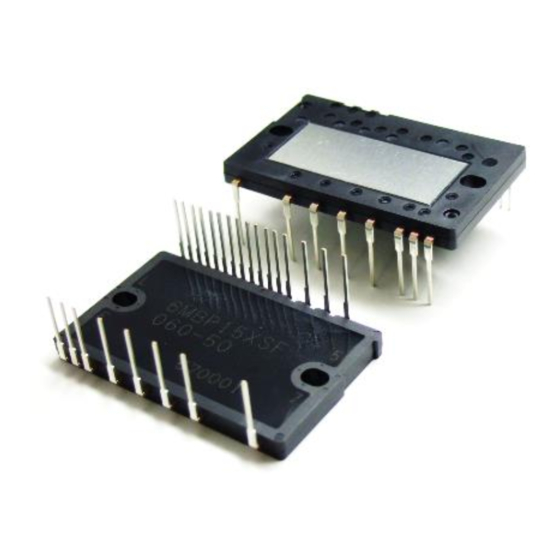
- Page 1 Fuji IGBT Intelligent-Power-Module “Small-IPM" Application Manual 6MBP15XS*060-50 6MBP20XS*060-50 6MBP30XS*060-50 6MBP35XS*060-50 Fuji Electric Co., Ltd. Dec. 2016 Fuji Electric Co., Ltd. MT6M12343 Rev.1.0 Dec.-2016...
-
Page 2: Table Of Contents
1. Soldering to PCB ................. 2. Mounting to Heat sink ................3. Cooler (Heat Sink) Selection..............Chapter 7 Cautions 1. Other warnings and precautions ............2. Handling and storage precautions ............3. Notice ....................Fuji Electric Co., Ltd. MT6M12343 Rev.1.0 Dec.-2016... - Page 3 Chapter 1 Product Outline Contents Page 1. Introduction ....................2. Product line-up ..................3. Definition of type name and marking spec ..........4. Package outline dimensions ..............5. Absolute maximum ratings ..............Fuji Electric Co., Ltd. MT6M12343 Rev.1.0 Dec.-2016...
-
Page 4: Introduction
The IPM doesn’t need insulated power supplies for the upper side drive because the IPM has built-in bootstrap diodes (BSD). VB(U) VB(V) VB(W) 3×HVIC IN(HU) 3×BSD IN(HV) 6×IGBT 6×FWD IN(HW) LVIC IN(LU) IN(LV) N(U) IN(LW) N(V) N(W) TEMP TEMP Fig. 1-1 Block Diagram of Internal Circuit Fuji Electric Co., Ltd. MT6M12343 Rev.1.0 Dec.-2016... - Page 5 Lead frame Mold resin Mold resin IGBT IGBT WIRE WIRE Mold resin Mold resin Aluminum base PCB with isolation layer Aluminum base PCB with isolation layer Fig.1-2 Package overview Fig.1-3 Package cross section diagram Fuji Electric Co., Ltd. MT6M12343 Rev.1.0 Dec.-2016...
-
Page 6: Product Line-Up
(Between shorted all terminals and case) ・Heat pump 6MBP15XSF060-50 applications ・Fan motor drive ・General motor drive 6MBP20XSD060-50 ・Servo drive 6MBP20XSF060-50 6MBP30XSD060-50 6MBP30XSF060-50 6MBP35XSD060-50 6MBP35XSF060-50 (LT): Temperature sensor output function (LT) (OH): Overheating protection function (OH) Fuji Electric Co., Ltd. MT6M12343 Rev.1.0 Dec.-2016... -
Page 7: Definition Of Type Name And Marking Spec
“” (Bank) : Japan M : Month (1 to 9 and O, N, D) P : Philippine NNNN : Serial number PRODUCT CODE TYPE NAME 6MBP15XSD060-50 6MBP15XSF060-50 6MBP20XSD060-50 6MBP20XSF060-50 6MBP30XSD060-50 6MBP30XSF060-50 6MBP35XSD060-50 6MBP35XSF060-50 Fig.1-4 Marking Specification Fuji Electric Co., Ltd. MT6M12343 Rev.1.0 Dec.-2016... -
Page 8: Package Outline Dimensions
It is improved of thermal conductivity between IMS and heat-sink. Pin No. Pin Name Pin No. Pin Name VB(U) N(W) VB(V) N(V) VB(W) N(U) IN(HU) IN(HV) IN(HW) IN(LU) IN(LV) IN(LW) Temp Fig.1-5. Case outline drawings Fuji Electric Co., Ltd. MT6M12343 Rev.1.0 Dec.-2016... -
Page 9: Absolute Maximum Ratings
C +150 j(max) of Inverter Block chips and the FWD chips Operating Junction Temperature Junction temperature of the IGBT and FWD C -40 ~ +150 of Inverter Block chips during continuous operation Fuji Electric Co., Ltd. MT6M12343 Rev.1.0 Dec.-2016... - Page 10 Maximum effective value of the sine-wave voltage between the terminals and the heat Isolation Voltage AC 1500 Vrms sink, when all terminals are shorted simultaneously. (Sine wave = 60Hz / 1min) Fuji Electric Co., Ltd. MT6M12343 Rev.1.0 Dec.-2016...
- Page 11 IPM. Furthermore, V is specified considering the margin of the surge voltage which is generated by the wiring (or pattern) stray inductance between the P-N(*) terminal and the capacitor. Fuji Electric Co., Ltd. MT6M12343 Rev.1.0 Dec.-2016...
-
Page 12: Description Of Terminal Symbols
Chapter 2 Description of Terminal Symbols and Terminology Contents Page 1. Description of Terminal Symbols ............2. Description of Terminology ..............Fuji Electric Co., Ltd. MT6M12343 Rev.1.0 Dec.-2016... - Page 13 Negative bus voltage input for W-phase N(V) Negative bus voltage input for V-phase N(U) Negative bus voltage input for U-phase Motor W-phase output Motor V-phase output Motor U-phase output Positive bus voltage input No Connection Fuji Electric Co., Ltd. MT6M12343 Rev.1.0 Dec.-2016...
-
Page 14: Description Of Terminology
Control signal pulse width necessary to change IGBT from OFF to ON. IN(on) width Refer Chapter 3 section 4. Operational input pulse Control signal pulse width necessary to change IGBT from ON to OFF. IN(off) width Refer Chapter 3 section 4. Fuji Electric Co., Ltd. MT6M12343 Rev.1.0 Dec.-2016... - Page 15 Resetting voltage at which the IGBT performs shut down when the upper side arm VB Under voltage reset level B(ON) IGBT bias voltage VB(*) drops. Refer chapter 3 section 2. VB Under voltage hysteresis Hysteresis voltage between V and V B(hys) B(OFF) B(ON) Fuji Electric Co., Ltd. MT6M12343 Rev.1.0 Dec.-2016...
- Page 16 Screwing torque when mounting the IPM to a heat sink with a specified screw. Heat-sink side flatness Flatness of a heat sink side. See Fig.2-3. 2.1V 0.8V d(off) d(on) c(off) c(on) Fig.2-1 Switching waveforms Fuji Electric Co., Ltd. MT6M12343 Rev.1.0 Dec.-2016...
- Page 17 Approx. 6.3 Heat sink side Tc measurement position SIDE VIEW TOP VIEW Fig.2-2 The measurement position of temperature sensor and T Measurement position Measurement position Fig.2-3 The measurement point of heat-sink side flatness. Fuji Electric Co., Ltd. MT6M12343 Rev.1.0 Dec.-2016...
- Page 18 4. Input Terminals IN(HU,HV,HW), IN(LU,LV,LW) ........3-13 5. Over Current Protection Input Terminal IS ..........3-16 6. Fault Status Output Terminal VFO ............3-17 7. Temperature Sensor Output Terminal TEMP ........... 3-18 8. Over Heating Protection ................3-20 Fuji Electric Co., Ltd. MT6M12343 Rev.1.0 Dec.-2016...
-
Page 19: Control Power Supply Terminals
Control circuit in this IPM might be damaged. If necessary, it is recommended to insert a Zener diode between each pair of control supply terminals. *1 N(*) : N(U), N(V), N(W) *2 VB(*) : VB(U)-U, VB(V)-V,VB(W)-W Fuji Electric Co., Ltd. MT6M12343 Rev.1.0 Dec.-2016... - Page 20 U , V , W (OH) Driver IGBT ( L ) Alarm timer N ( U , V , W ) Fig.3-1 Control supply of high and low side V UV Circuit Fuji Electric Co., Ltd. MT6M12343 Rev.1.0 Dec.-2016...
- Page 21 <4> When the voltage drop time is more than t , the fault output pulse width is generated and all lower side IGBTs are OFF state regardless of the input signal condition during the same time. Fuji Electric Co., Ltd. MT6M12343 Rev.1.0 Dec.-2016...
- Page 22 V , the upper side IGBT remains OFF state. CCH(OFF) But the fault output VFO keeps high level. <3> The HVIC starts to operate from the next input signal after UV is reset. Fuji Electric Co., Ltd. MT6M12343 Rev.1.0 Dec.-2016...
-
Page 23: Power Supply Terminals Of High Side Vb(U,V,W)
Over 20 Control circuit in the IPM might be damaged. It is recommended to insert a Zener diode between each pair of high side power supply terminals. Fuji Electric Co., Ltd. MT6M12343 Rev.1.0 Dec.-2016... - Page 24 U , V , W < LVIC > U , V , W Alarm timer IGBT ( L ) N ( U , V , W ) Fig.3-4 Control supply of high side VB(*) UV protection circuit Fuji Electric Co., Ltd. MT6M12343 Rev.1.0 Dec.-2016...
- Page 25 , the upper side IGBT remains OFF state. B(OFF) But the fault output VFO keeps high level. <3> The HVIC starts to operate from the next input signal after UV is reset. *1 VB(*) : VB(U)-U,VB(V)-V,VB(W)-W Fuji Electric Co., Ltd. MT6M12343 Rev.1.0 Dec.-2016...
-
Page 26: Function Of Internal Bsds (Bootstrap Diodes)
Gate signal of Lower side IGBT Declining due to current consumed by drive circuit of the upper side IGBT b(t1) Voltage level of bootstrap capacitor Spontaneous discharge of C Fig.3-7 Timing chart of Charging operation Fuji Electric Co., Ltd. MT6M12343 Rev.1.0 Dec.-2016... - Page 27 Voltage level of bootstrap capacitor (Vb) Declining due to current consumed by drive circuit of upper side IGBT Fig.3-9 Timing chart of Charging operation under the lower side arm FWD is ON Fuji Electric Co., Ltd. MT6M12343 Rev.1.0 3-10 Dec.-2016...
- Page 28 Gate signal of Lower side IGBT Voltage level of bootstrap capacitor (Vb) Declining due to current consumed by drive circuit of upper side IGBT Fig.3-10 Timing chart of Charging and Discharging operation Fuji Electric Co., Ltd. MT6M12343 Rev.1.0 3-11 Dec.-2016...
- Page 29 Main Bus voltage (P-N) HVICs and LVIC supply voltage Start Upper side IGBT supply voltage Vb(*) Gate signal of Lower side IGBT Initial charging time Fig.3-12 Timing chart of initial charging operation Fuji Electric Co., Ltd. MT6M12343 Rev.1.0 3-12 Dec.-2016...
- Page 30 Fig.3-13 VF-IF curve of boot strap diode Typical BSD Built-in limiting resistance Characteristics IF=f(VF):80 s pulse test 1000 -40°c 25°c 125°c Forward Voltage: VF [V] Fig.3-14 Equivalent series resistance of boot strap diode Fuji Electric Co., Ltd. MT6M12343 Rev.1.0 3-13 Dec.-2016...
-
Page 31: Input Terminals In(Hu,Hv,Hw), In(Lu,Lv,Lw)
IN ( HU ) , IN ( HV ) , IN ( HW ) IN ( LU ) , IN ( LV ) , IN ( LW ) Fig.3-15 Recommended MPU I/O Interface Circuit of IN(HU,HV,HW), IN(LU,LV,LW) terminals Fuji Electric Co., Ltd. MT6M12343 Rev.1.0 3-14... - Page 32 U , V , W Input IN ( LV ) Noise Delay Driver IN ( LW ) Filter IGBT ( L ) N ( U , V , W ) Fig.3-16 Input terminals IN(HU,HV,HW), IN(LU,LV,LW) Circuit Fuji Electric Co., Ltd. MT6M12343 Rev.1.0 3-15 Dec.-2016...
- Page 33 Minimum IN(ON) Fig.3-17 IGBT drive state versus ON pulse width of Control signal Out recommended Recommended range range Minimum IN(OFF) Fig.3-18 IGBT drive state versus OFF pulse width of Control signal Fuji Electric Co., Ltd. MT6M12343 Rev.1.0 3-16 Dec.-2016...
-
Page 34: Over Current Protection Input Terminal Is
. Inherently there is dead time of LVIC in t d(IS) d(IS) t4 : After the fault output pulse width t , the OC is reset. Then next input signal is activated. Fuji Electric Co., Ltd. MT6M12343 Rev.1.0 3-17 Dec.-2016... -
Page 35: Fault Status Output Terminal Vfo
Fig.3-21 Recommended MPU I/O Interface Circuit of VFO terminal 0.16 0.14 0.12 0.10 0.08 0.06 0.04 10kΩ resistance to 5V pull-up 0.02 0.00 IFO[mA] Fig.3-22 Voltage-current Characteristics of VFO terminal at the fault state condition Fuji Electric Co., Ltd. MT6M12343 Rev.1.0 3-18 Dec.-2016... -
Page 36: Temperature Sensor Output Terminal Temp
V(temp)=f(Tj);V (*)=15V -40 -25 Junction Temperature of LVIC:Tj(LVIC) [°c] Fig.3-24 LVIC temperature vs. TEMP output Fig.3-24 LVIC temperature vs. TEMP output voltage characteristics with 22kΩ pull-down resistor voltage characteristics without pull-down resistor Fuji Electric Co., Ltd. MT6M12343 Rev.1.0 3-19 Dec.-2016... - Page 37 TEMP terminal voltage is the clamp voltage even though is above V CCL(ON) : TEMP function is reset when V falls below V . TEMP terminal voltage is the same as CCL(OFF) the clamp voltage. Fuji Electric Co., Ltd. MT6M12343 Rev.1.0 3-20 Dec.-2016...
-
Page 38: Over Heating Protection
: The fault status, which outputs over t , is reset and next input signal is activated, when LVIC – T temperature falls below T which is the case overheating protection hysteresis. OH(hys) Fuji Electric Co., Ltd. MT6M12343 Rev.1.0 3-21 Dec.-2016... -
Page 39: Connection Of Bus Input Terminal And Low Side Emitters
Chapter 4 Power Terminals Contents Page 1. Connection of Bus Input terminal and Low Side Emitters...... 2. Setting of Shunt Resistor of Over Current Protection ......Fuji Electric Co., Ltd. MT6M12343 Rev.1.0 Dec.-2016... - Page 40 "A" or "C", location "C" is a reasonable position considering the impact to the current N(U) sensing accuracy. Therefore, location "C" is DC Bus N(V) recommended. Negative N(W) Shunt resistor Fig.4-1 Recommended wiring of shunt resistor and snubber capacitor Fuji Electric Co., Ltd. MT6M12343 Rev.1.0 Dec.-2016...
-
Page 41: Setting Of Shunt Resistor Of Over Current Protection
(4.4) total delay d(IS) The short circuit withstands capability of IGBT must be considered for the total delay time t total Please confirm the proper delay time in actual equipment. Fuji Electric Co., Ltd. MT6M12343 Rev.1.0 Dec.-2016... -
Page 42: Examples Of Application Circuits
Chapter 5 Recommended wiring and layout Contents Page 1. Examples of Application Circuits............2. Recommendation and Precautions in PCB design......Fuji Electric Co., Ltd. MT6M12343 Rev.1.0 Dec.-2016... - Page 43 IGBT malfunction. Long wiring here might cause OC level fluctuation and malfunction. Fig. 5-1 Example of application circuit 1 (In case of sensing all 3 phase currents at once with a single shunt resistor) Fuji Electric Co., Ltd. MT6M12343 Rev.1.0 Dec.-2016...
- Page 44 10nH. input and cause Vref=V IS(ref) IGBT malfunction. Long wiring here might cause OC level fluctuation and malfunction. Fig. 5-2 Example of application circuit 2 (In case of sensing each phase current individually) Fuji Electric Co., Ltd. MT6M12343 Rev.1.0 Dec.-2016...
- Page 45 If signal GND is connected to power GND by board pattern, there is possibilty of malfunction due to fluctuations at the power GND. It is recommended to connect signal GND and power GND at a single point. Fuji Electric Co., Ltd. MT6M12343 Rev.1.0 Dec.-2016...
-
Page 46: Recommendation And Precautions In Pcb Design
SGND IN(LV) IN(LW) VCCL N(U) Over current protection SGND N(V) N(W) TEMP Power input note) The input signals are represented with "IN(HU)". Fig.5-3 Image of recommended PCB layout (Overall design around the IPM) Fuji Electric Co., Ltd. MT6M12343 Rev.1.0 Dec.-2016... - Page 47 Zener diode between VB(U) and U are Fig.5-5 Image of recommended PCB layout recommended. It should be connected (Power supply for high side drive part) close to VB(U) terminal. (The same applies to VB(V) and VB(W).) Fuji Electric Co., Ltd. MT6M12343 Rev.1.0 Dec.-2016...
- Page 48 (E) The pattern of Signal GND from system control and the pattern from COM terminal should be connected at single point ground. The single point ground should be as close to the COM terminal as possible. Fuji Electric Co., Ltd. MT6M12343 Rev.1.0 Dec.-2016...
- Page 49 The single point ground should be as close to the shunt resistors as possible. The other precautions and recommendations are same as Fig.5-7 (a). Please refer to Chapter 4, Section 2 for more information on the circuit constant determination. Fuji Electric Co., Ltd. MT6M12343 Rev.1.0 Dec.-2016...
- Page 50 Chapter 6 Mounting Guideline and Thermal Design Contents Page 1. Soldering to PCB ................2. Mounting to Heat sink ................. 3. Cooler (Heat Sink) Selection............... Fuji Electric Co., Ltd. MT6M12343 Rev.1.0 Dec.-2016...
-
Page 51: Soldering To Pcb
It is not recommended to reuse the device after it is removed from the circuit board. There is a possibility that the removed device was subjected to thermal or mechanical damage during the removal process. Fuji Electric Co., Ltd. MT6M12343 Rev.1.0 Dec.-2016... -
Page 52: Mounting To Heat Sink
Application position : 7.5mm apart from the eadge of aluminum base ±0.5 Application quantity : 0.03g DETAIL A DETAIL B Center line of Thermal compound Aluminum base 7.5mm 7.5mm Fig.6-3 Recommended an application position and application quantity. Fuji Electric Co., Ltd. MT6M12343 Rev.1.0 Dec.-2016... -
Page 53: Cooler (Heat Sink) Selection
For more detail about thermal design, please refer Chapter 6 Section 2 of this note and “IGBT MODULE APPLICATION MANUAL (REH984c)” Contents: • Power dissipation loss calculation • Selecting heat sinks • Heat sink mounting precautions • Troubleshooting Fuji Electric Co., Ltd. MT6M12343 Rev.1.0 Dec.-2016... -
Page 54: Notice
Chapter 7 Cautions Contents Page 1. Precautions for use ................2. Precautions on storage ..............3. Notice ....................Fuji Electric Co., Ltd. MT6M12343 Rev.1.0 Dec.-2016... - Page 55 Make sure in your design that during open short test, high voltage will not be applied to the low terminals. To avoid accidents and explosion damage if high voltage is applied, use fuses in your design. Fuji Electric Co., Ltd. MT6M12343 Rev.1.0 Dec.-2016...
- Page 56 The IPM should be stored with the lead terminals remaining unprocessed. Rust may cause presoldered connections to fail during later processing. • The IPM should be stored in antistatic containers or shipping bags. • Under the above storage condition, the shelf life is one year. Fuji Electric Co., Ltd. MT6M12343 Rev.1.0 Dec.-2016...
- Page 57 If you have any question about any portion of this application note, ask Fuji Electric Co., Ltd. or its sales agencies. Neither Fuji Electric Co., Ltd. nor its agencies shall be liable for any injury or damage caused by any use of the products not in accordance with instructions set forth herein.
Need help?
Do you have a question about the Small-IPM Series and is the answer not in the manual?
Questions and answers