Table of Contents
Advertisement
Quick Links
www.ti.com
User's Guide
DAC12DL3200 Evaluation Module
The DAC12DL3200 evaluation module (EVM) is used to evaluate the DAC12DL3200 digital-to-analog converter
(DAC) from Texas Instruments. Throughout this document, the terms evaluation board, evaluation module, and
EVM are synonymous with the DAC12DL3200EVM.
1
Introduction.............................................................................................................................................................................2
1.1 Low Latency Evaluation of Receive and Transmit.............................................................................................................
Documentation......................................................................................................................................................4
2 Equipment...............................................................................................................................................................................
2.2 Required Equipment..........................................................................................................................................................
3 Setup Procedure.....................................................................................................................................................................
3.1 Install the High Speed Data Converter (HSDC) Pro Software...........................................................................................
3.3 Connect the DAC12DL3200EVM and TSW14DL3200EVM..............................................................................................
3.4 Connect the Power Supplies to the Boards (Power Off)....................................................................................................
3.5 Connect the Signal Generators to the EVM (*RF Outputs Disabled Until Directed)..........................................................
3.7 Turn On the DAC12DL3200EVM 5-V Power Supply and Connect to the PC....................................................................
3.10 Open the HSDC Software and Load the FPGA Image to the TSW14DL3200EVM.......................................................
Adjustment...........................................................................................................................................14
Operation....................................................................................................................................................17
4.1 Single-Channel RF Mode 2 (2nd Nyquist Zone)..............................................................................................................
4.2 Dual-Channel Output Mode 0..........................................................................................................................................
4.3 Dual Channel Mode1 Setup.............................................................................................................................................
4.5 Direct Digital Synthesis Mode..........................................................................................................................................
File...................................................................................................................................................................21
Configuration............................................................................................................................................................22
6.1 Tab Organization..............................................................................................................................................................
6.2 Low-Level Control............................................................................................................................................................
A Troubleshooting the DAC12DL3200EVM...........................................................................................................................
B DAC12DL3200EVM Onboard Clocking Configuration......................................................................................................
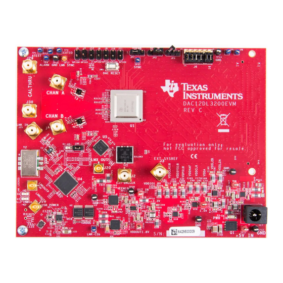
Figure 1-1. DAC12DL3200EVM..................................................................................................................................................
Figure 1-2. Low Latency LVDS-Based ADC Receiver and DAC Transmitter..............................................................................
Figure 1-3. Low Latency ADC EVM, Capture Card and Pattern Generator, and DAC EVM.......................................................
Figure 2-1. DAC12DL3200EVM Features...................................................................................................................................
Setup.........................................................................................................................................................6
Figure 3-2. Configuration GUI: LMK04828 Tab...........................................................................................................................
Figure 3-4. Selecting Configuration File....................................................................................................................................
Figure 3-5. No Firmware Loaded...............................................................................................................................................
Figure 3-6. Selecting DAC Mode 2............................................................................................................................................
Figure 3-8. IO Delay..................................................................................................................................................................
SBAU374 - MAY 2021
Submit Document Feedback
Table of Contents
Summary.............................................................................................................4
Software...............................................................................................................................7
Outputs.........................................................................................................................8
Setup..........................................................................................................................18
List of Figures
Tab.................................................................................................................................................10
Setup..............................................................................................................................................13
Copyright © 2021 Texas Instruments Incorporated
ABSTRACT
PC..............................................................................8
Table of Contents
DAC12DL3200 Evaluation Module
3
4
5
6
7
7
7
8
8
9
11
17
17
18
18
22
22
24
25
2
3
3
4
9
10
11
12
14
1
Advertisement
Table of Contents

Related Manuals for Texas Instruments DAC12DL3200


Summary of Contents for Texas Instruments DAC12DL3200
-
Page 1: Table Of Contents
User’s Guide DAC12DL3200 Evaluation Module ABSTRACT The DAC12DL3200 evaluation module (EVM) is used to evaluate the DAC12DL3200 digital-to-analog converter (DAC) from Texas Instruments. Throughout this document, the terms evaluation board, evaluation module, and EVM are synonymous with the DAC12DL3200EVM. Table of Contents Introduction.....................................2... -
Page 2: Introduction
Software GUI, is used to send LVDS data test patterns to the DAC12DL3200EVM. With proper hardware selection in the HSDC Pro software, the TSW14DL3200EVM is automatically configured to support the different modes of operation of the DAC12DL3200. The interface provides LVDS output data up to 1600 MSPS. -
Page 3: Low Latency Evaluation Of Receive And Transmit
ADC12DL3200 device and the samples are extracted and collected by the FPGA. These samples are then forwarded to the DAC12DL3200 which generates the resultant output signal (delayed version of the input test signal). The IO architecture of the Xilinx UltraScale enables extremely high-speed data rates by trading off latency for throughput. -
Page 4: Related Documentation
TSW14DL3200EVM User's Guide ADC12DL3200EVM User's Guide for configuration and status information. 2 Equipment This section describes the equipment needed to evaluate the full performance of the DAC12DL3200 device. 2.1 Evaluation Board Feature Identification Summary Figure 2-1 shows the EVM features. Note The EVM does not have any power sequencing as the EVM was designed before this requirement was added to the data sheet. -
Page 5: Required Equipment
By default, the DAC12DL3200EVM uses an external clocking solution. A few small board modifications enable the onboard clocking solution. If onboard clocking is used, no signal generators are required. SBAU374 – MAY 2021 DAC12DL3200 Evaluation Module Submit Document Feedback Copyright © 2021 Texas Instruments Incorporated... -
Page 6: Setup Procedure
Figure 3-1. EVM Test Setup Note The HSDC Pro software must be installed before connecting the TSW14DL3200EVM to the PC for the first time. DAC12DL3200 Evaluation Module SBAU374 – MAY 2021 Submit Document Feedback Copyright © 2021 Texas Instruments Incorporated... -
Page 7: Install The High Speed Data Converter (Hsdc) Pro Software
Make sure that the 12-V power supply is connected to the TSW14DL3200EVM and not the DAC12DL3200EVM. Providing the DAC12DL3200EVM with 12-V may result in immediate damage. Leave the TSW14DL3200EVM power switch in the off position. SBAU374 – MAY 2021 DAC12DL3200 Evaluation Module Submit Document Feedback Copyright © 2021 Texas Instruments Incorporated... -
Page 8: Connect The Signal Generators To The Evm (*Rf Outputs Disabled Until Directed)
4. Turn on the power switch on the TSW14DL3200EVM 3.8 Turn On the Signal Generator RF Outputs Turn on the signal output of the two signal generators connected to the DAC12DL3200EVM. DAC12DL3200 Evaluation Module SBAU374 – MAY 2021 Submit Document Feedback Copyright © 2021 Texas Instruments Incorporated... -
Page 9: Open The Dac12Dl3200Evm Gui And Program The Dac And Clocks For Single Channel, Nrz Mode 2 Operation
Figure 3-2. Configuration GUI: LMK04828 Tab 1. Open the DACDL3200EVM GUI by clicking on the DAC12DL3200 GUI icon and run as administrator. 2. Verify the USB has connected to the board. This is indicated by a green USB Status indicator in the top right corner of the GUI. -
Page 10: Figure 3-3. Low Level View Tab
This configuration file sets up the DAC to operate in a single-channel mode with the output available only on CHA. The same output is available on CHB in this mode if desired, but the configuration file has CHB powered down by default. DAC12DL3200 Evaluation Module SBAU374 – MAY 2021 Submit Document Feedback Copyright © 2021 Texas Instruments Incorporated... -
Page 11: Open The Hsdc Software And Load The Fpga Image To The Tsw14Dl3200Evm
2. Click on the DAC tab in the top right of the GUI. In the device drop-down menu, select "DAC12DL3200_MODE2_12b_sync_istrb” as illustrated in Figure 3-6. SBAU374 – MAY 2021 DAC12DL3200 Evaluation Module Submit Document Feedback Copyright © 2021 Texas Instruments Incorporated... -
Page 12: Figure 3-6. Selecting Dac Mode 2
5. Set the tone center "1GHz" in the I/Q Multitone Generator window in the lower left of the GUI, . 6. Enter the # of tones "1", also in the I/Q Multitone Generator window 7. Click the Create Tones button. DAC12DL3200 Evaluation Module SBAU374 – MAY 2021 Submit Document Feedback Copyright © 2021 Texas Instruments Incorporated... -
Page 13: Figure 3-7. Hsdc Pro Gui Setup
Setup Procedure The setup looks as shown in Figure 3-7. Figure 3-7. HSDC Pro GUI Setup SBAU374 – MAY 2021 DAC12DL3200 Evaluation Module Submit Document Feedback Copyright © 2021 Texas Instruments Incorporated... -
Page 14: Dxstrb Timing Adjustment
3-9. Click the Write Registers button. Enter x10000004 for the RegAddress in the Read section. Click the Read Registers button. Verify x8000 was written to this address. Close this window. DAC12DL3200 Evaluation Module SBAU374 – MAY 2021 Submit Document Feedback Copyright © 2021 Texas Instruments Incorporated... -
Page 15: Figure 3-9. Io Delay Register Write
In the HSDC Pro GUI main page, click the Send button in the upper left to send the test tone to the DAC EVM. There should now be a 1-GHz output tone on CHA SMA connector J1. SBAU374 – MAY 2021 DAC12DL3200 Evaluation Module Submit Document Feedback Copyright © 2021 Texas Instruments Incorporated... -
Page 16: Figure 3-10. Dac Channel A Output
Setup Procedure www.ti.com Figure 3-10. DAC Channel A Output DAC12DL3200 Evaluation Module SBAU374 – MAY 2021 Submit Document Feedback Copyright © 2021 Texas Instruments Incorporated... -
Page 17: Other Modes Of Operation
4.1 Single-Channel RF Mode 2 (2nd Nyquist Zone) In the DAC GUI, click on the DAC12DL3200 → DACA tab. For single DAC operation in the 2nd Nyquist zone, in the DACA_output mode box, select RF mode. With the DAC sampling at 6.4 GHz, and with an input tone at 2.6 GHz, the image will be located at 3.8 GHz in the 2nd Nyquist. -
Page 18: Dual Channel Mode1 Setup
Nyquist, which is located at 7.4 GHz and 11.8 GHz in the 4th Nyquist zone. 4.5 Direct Digital Synthesis Mode The DAC12DL3200 contains two numerically controlled oscillators (NCOs) that can optionally be used for direct digital synthesis of tones for each DAC. There are two NCO banks, each with 16 separate 32-bit NCOs. The banks can be used separately for each DAC, or together to provide 32 NCOs for one DAC. -
Page 19: Figure 4-2. Daca Tab With Nco Settings
The same instructions apply for setting the NCO phase. The value to be entered for phase is in radians. The valid entries are from –3.1416 to 3.1416. The equation for this setting can be found in the device data sheet. SBAU374 – MAY 2021 DAC12DL3200 Evaluation Module Submit Document Feedback Copyright © 2021 Texas Instruments Incorporated... -
Page 20: Figure 4-3. Ncoa Calculation
If using the SPI_SYNC for the NCO SYNC source, after making any changes to the NCO settings, click on the SPI_SYNC button twice to synchronize the two NCOs. Figure 4-3. NCOA Calculation DAC12DL3200 Evaluation Module SBAU374 – MAY 2021 Submit Document Feedback Copyright © 2021 Texas Instruments Incorporated... -
Page 21: Register Log File
GUI, the log file updates and shows the actual register address and data value that was written to the DAC12DL3200, LMK04828, or LMX2592. This log file information can be saved by first highlighting the register settings to be saved then double clicking inside the log file and selecting Save Selected. -
Page 22: Device Configuration
FTDI USB-to-SPI converter located on the EVM. The GUI is used to write instructions on the bus and program the registers of the DAC12DL3200, LMK04828, and LMX2592 devices. For more information about the registers in the DAC device, see the DAC12DL3200 6.4-GSPS Single Channel... -
Page 23: Table 6-1. Low-Level Controls
Perform a generic read or write command to the device shown in the Block drop-down menu using the read or write register buttons address and write data information SBAU374 – MAY 2021 DAC12DL3200 Evaluation Module Submit Document Feedback Copyright © 2021 Texas Instruments Incorporated... -
Page 24: A Troubleshooting The Dac12Dl3200Evm
• Use the free FT_PROG software from FTDI chip and verify that the onboard FTDI chip is programmed Configuration GUI is not able with the product description DAC12DL3200. to connect to the EVM • Verify that the TSW14DL3200EVM is properly connected to the PC with a mini USB 3.0 cable and that the board serial number is properly identified by the HSDC software. -
Page 25: B Dac12Dl3200Evm Onboard Clocking Configuration
Figure B-1. Onboard Clocking Setup 4. Remove the signal generators. 5. Program the DAC using the DAC12DL3200 GUI. a. Press the DAC RESET switch on the EVM. b. In the DAC GUI Low Level View tab, select the configuration file called "LMK_100M_LMX_6400M_Mode2_NRZ_Single_DAC.cfg". -
Page 26: Figure B-2. Default Board Clock Configuration Circuit
The LMX2582 and LMK04828 may be reconfigured to exercise more features, but this EVM is not intended to be a full evaluation platform for these devices. For a full evaluation platform, see the LMK04828EVM tool folder LMX2592EVM tool folder. DAC12DL3200 Evaluation Module SBAU374 – MAY 2021 Submit Document Feedback Copyright © 2021 Texas Instruments Incorporated... - Page 27 STANDARD TERMS FOR EVALUATION MODULES Delivery: TI delivers TI evaluation boards, kits, or modules, including any accompanying demonstration software, components, and/or documentation which may be provided together or separately (collectively, an “EVM” or “EVMs”) to the User (“User”) in accordance with the terms set forth herein.
- Page 28 www.ti.com Regulatory Notices: 3.1 United States 3.1.1 Notice applicable to EVMs not FCC-Approved: FCC NOTICE: This kit is designed to allow product developers to evaluate electronic components, circuitry, or software associated with the kit to determine whether to incorporate such items in a finished product and software developers to write software applications for use with the end product.
- Page 29 www.ti.com Concernant les EVMs avec antennes détachables Conformément à la réglementation d'Industrie Canada, le présent émetteur radio peut fonctionner avec une antenne d'un type et d'un gain maximal (ou inférieur) approuvé pour l'émetteur par Industrie Canada. Dans le but de réduire les risques de brouillage radioélectrique à...
- Page 30 www.ti.com EVM Use Restrictions and Warnings: 4.1 EVMS ARE NOT FOR USE IN FUNCTIONAL SAFETY AND/OR SAFETY CRITICAL EVALUATIONS, INCLUDING BUT NOT LIMITED TO EVALUATIONS OF LIFE SUPPORT APPLICATIONS. 4.2 User must read and apply the user guide and other available documentation provided by TI regarding the EVM prior to handling or using the EVM, including without limitation any warning or restriction notices.
- Page 31 Notwithstanding the foregoing, any judgment may be enforced in any United States or foreign court, and TI may seek injunctive relief in any United States or foreign court. Mailing Address: Texas Instruments, Post Office Box 655303, Dallas, Texas 75265 Copyright © 2019, Texas Instruments Incorporated...
- Page 32 TI products. TI’s provision of these resources does not expand or otherwise alter TI’s applicable warranties or warranty disclaimers for TI products.IMPORTANT NOTICE Mailing Address: Texas Instruments, Post Office Box 655303, Dallas, Texas 75265 Copyright © 2021, Texas Instruments Incorporated...
Need help?
Do you have a question about the DAC12DL3200 and is the answer not in the manual?
Questions and answers