Table of Contents
Advertisement
Quick Links
1
1.1
1.2
2
2.1
2.2
3
3.1
3.2
3.3
3.4
3.5
4
4.1
4.2
4.3
4.4
4.5
.................................................................................................................
5
5.1
5.2
1
2
3
4
5
6
7
8
9
10
11
12
13
14
15
16
17
18
TSW3100 CommSignalPattern (WCDMA) Programming GUI for DAC3482, DAC34H84, and
SLAU432 - February 2012
Submit Documentation Feedback
..................................................................................................................
............................................................................................................
...............................................................................................
............................................................................................................
............................................................................................
................................................................................................
...................................................................................
..............................................................................................
..........................................................................................
...................................................................................
..............................................................................................
..........................................................................................
............................................................................................
........................................................................................................
...........................................................................................................
.......................................................................................................
.....................................................................................................
............................................................................................................
..................................................................................................
.............................................................................................
....................................................................................
Copyright © 2012, Texas Instruments Incorporated
Contents
..............................................................................
..........................................................................
..........................................................................
..............................................................................
..........................................................................
..........................................................................
...................................................................
.......................................................................
List of Figures
.......................................................................
..............................................................................
................................................................
................................................................
..............................................................................
User's Guide
SLAU432 - February 2012
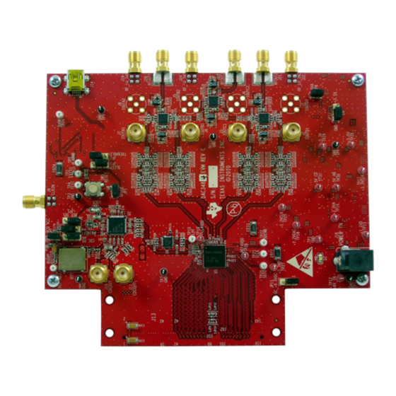
DAC348x EVM
........................................
...........................
......................................
DAC348x EVM
2
2
2
3
3
4
11
11
11
12
12
13
16
16
16
17
17
17
20
20
20
3
4
6
7
8
9
10
11
12
13
13
14
15
15
16
17
18
1
Advertisement
Table of Contents

Related Manuals for Texas Instruments DAC348 Series


Summary of Contents for Texas Instruments DAC348 Series
-
Page 1: Table Of Contents
TSW3100 FPGA Clock 100-Ω LVDS Termination at Pins T31 and T32 of the FPGA ................Test Set-up Block Diagram for TSW3100 ........TSW3100 CommSignalPattern (WCDMA) Programming GUI for DAC3484 TSW3100 CommSignalPattern (WCDMA) Programming GUI for DAC3482, DAC34H84, and SLAU432 – February 2012 DAC348x EVM Submit Documentation Feedback Copyright © 2012, Texas Instruments Incorporated... -
Page 2: Introduction
TSW1400EVM (or TSW3100EVM) as FPGA reference clocks. The EVM can be used along with Texas Instruments TSW1400 or TSW3100 with limited data rate support (up to 1.25GSPS LVDS Bus rate) to perform a wide varieties of test and measurements. The TSW1400 generates the test patterns that are fed to the DAC348x through a maximum 1.5 GSPS LVDS Bus port. -
Page 3: Software Control
Follow the on-screen instructions • Once installed, launch the program by clicking on the DAC348x_GUI_vxpx program in Start>Texas Instruments DACs. The installation directory is located at C:\Program Files\Texas SLAU432 – February 2012 DAC348x EVM Submit Documentation Feedback Copyright © 2012, Texas Instruments Incorporated... -
Page 4: Software Operation
Parity: provides configuration of the parity input. • PLL Settings: provides configuration of the on-chip PLL circuitry. • Temperature Sensor: provides temperature monitoring of DAC3484/2 die temperature. SLAU432 – February 2012 DAC348x EVM Submit Documentation Feedback Copyright © 2012, Texas Instruments Incorporated... - Page 5 PCB can be added to the LVDS DATACLK PCB trace length. Set SJP9, SJP10, SJP11, and SJP12 to 2-3 position for approximately 220ps of trace delay. SLAU432 – February 2012 DAC348x EVM Submit Documentation Feedback Copyright © 2012, Texas Instruments Incorporated...
-
Page 6: Pll Configuration
(b) If stability (P x M) is greater than 120, then set to “Double” or install external loop filter 8. Adjust the Freq. Tune (coarse tune) accordingly. For additional information, see the relevant DAC348x data sheet. SLAU432 – February 2012 DAC348x EVM Submit Documentation Feedback Copyright © 2012, Texas Instruments Incorporated... -
Page 7: Digital Block Options
– REGWR: auto-sync from SIF register write. If this option is chosen, the GUI automatically synchronizes the offset adjustment with each value update by writing to 0x10 (QMC phase AB) or 0x11 (QMC phase CD) registers last. SLAU432 – February 2012 DAC348x EVM Submit Documentation Feedback Copyright © 2012, Texas Instruments Incorporated... -
Page 8: Output Control Options
– DAC Gain = 10 for 20mA full-scale current (default). • Output Shutoff On: allows outputs to shut-off when DACCLK GONE, DATACLK GONE, or FIFO COLLISION alarm event occurs. SLAU432 – February 2012 DAC348x EVM Submit Documentation Feedback Copyright © 2012, Texas Instruments Incorporated... -
Page 9: Cdce62005 Tab Configured For 4X Interpolation
Y4: FPGA Clock 2. This clock is an ac coupled LVDS. This clock must be enabled when using the DAC34H84 and DAC34SH84 with the TSW1400. The clock rate for this should be F /interpolation/4 for DAC34H84, and DAC34SH84 SLAU432 – February 2012 DAC348x EVM Submit Documentation Feedback Copyright © 2012, Texas Instruments Incorporated... -
Page 10: Usb Port Reset
Read All: Reads register configuration from DAC348x device • Load Regs: Load a register file for all devices. Sample configuration files for common frequency plans are located in the install directory: C:\Programs Files\Texas Instruments\DAC348x\EVM Configuration File Released. – Select Load Regs button. -
Page 11: Basic Test Procedure With Tsw1400
The test set-up for general testing of the DAC348x with the TSW1400 pattern generation card is shown in Figure Signal Generator (CLK Source) DAC348X Spectrum TSW1400 Analyzer Figure 8. Test Set-up Block Diagram for TSW1400 SLAU432 – February 2012 DAC348x EVM Submit Documentation Feedback Copyright © 2012, Texas Instruments Incorporated... -
Page 12: Test Setup Connection
DAC3484 running at 1228.8MSPS. Load this file and wait a couple of seconds for the settings to go into effect. The DAC3482, DAC34H84, and DAC34SH84 equivalent example files are also available in the installation folder. SLAU432 – February 2012 DAC348x EVM Submit Documentation Feedback Copyright © 2012, Texas Instruments Incorporated... -
Page 13: Tsw1400 Example Setup Procedure
Figure 11. Load DAC Firmware Prompt 3. Click on the button labeled “Load File to transfer into TSW 1400”, located near the top left of the GUI. SLAU432 – February 2012 DAC348x EVM Submit Documentation Feedback Copyright © 2012, Texas Instruments Incorporated... -
Page 14: Load File To Transfer Into Tsw1400
Figure 12. Load File to Transfer into TSW1400 4. Select the file "WCDMA_TM1_complexIF30MHz_Fdata307.2MHz_1000.tsw" under C:\Program Files\Texas Instruments\High Speed Data Converter Pro\1400 Details\Testfiles. The data rate of the file selected will depend on the sampling rate and interpolation ratio of the DAC configuration. -
Page 15: Dac348X Transformer Coupled Output At 60Mhz If
U p p e r - 8 2 . 9 7 (baseband = 30MHz, NCO disabled, QMC Gain = 1024) Figure 14. DAC348x Transformer Coupled Output at 30MHz IF SLAU432 – February 2012 DAC348x EVM Submit Documentation Feedback Copyright © 2012, Texas Instruments Incorporated... -
Page 16: Basic Test Procedure With Tsw3100
Figure 15. TSW3100 FPGA Clock 100-Ω LVDS Termination at Pins T31 and T32 of the FPGA Test Block Diagram for TSW3100 The test set-up for general testing of the DAC348x with the TSW3100 pattern generation card is shown in Figure SLAU432 – February 2012 DAC348x EVM Submit Documentation Feedback Copyright © 2012, Texas Instruments Incorporated... -
Page 17: Test Set-Up Connection
Enter desired Offset Frequency (i.e. 30 MHz) for each desired carrier • Select the 16b QDAC output button for DAC3484 (see Figure 17) or LVDS output button for DAC3482, DAC34H84, and DAC34SH84 (see Figure 18). SLAU432 – February 2012 DAC348x EVM Submit Documentation Feedback Copyright © 2012, Texas Instruments Incorporated... -
Page 18: Tsw3100 Commsignalpattern (Wcdma) Programming Gui For Dac3484
The expect results are shown in Figure 13 (NCO enabled at 30MHz) and Figure 14 (NCO disabled). Figure 17. TSW3100 CommSignalPattern (WCDMA) Programming GUI for DAC3484 SLAU432 – February 2012 DAC348x EVM Submit Documentation Feedback Copyright © 2012, Texas Instruments Incorporated... - Page 19 Basic Test Procedure with TSW3100 www.ti.com Figure 18. TSW3100 CommSignalPattern (WCDMA) Programming GUI for DAC3482, DAC34H84, and DAC34SH84 SLAU432 – February 2012 DAC348x EVM Submit Documentation Feedback Copyright © 2012, Texas Instruments Incorporated...
-
Page 20: References
FMC-DAC-ADAPTER Physical Design Database Rev D Board (SLOR102) DAC34H84EVM Design Package board rev C (SLAC518) DAC348x EVM Software (SLAC483) High Speed Data Converter Pro software (SLWC107) SLAU432 – February 2012 DAC348x EVM Submit Documentation Feedback Copyright © 2012, Texas Instruments Incorporated... - Page 21 Any exceptions to this is strictly prohibited and unauthorized by Texas Instruments unless user has obtained appropriate experimental/development licenses from local regulatory authorities, which is responsibility of user including its acceptable authorization.
- Page 22 REGULATORY COMPLIANCE INFORMATION (continued) FCC Interference Statement for Class B EVM devices This equipment has been tested and found to comply with the limits for a Class B digital device, pursuant to part 15 of the FCC Rules. These limits are designed to provide reasonable protection against harmful interference in a residential installation. This equipment generates, uses and can radiate radio frequency energy and, if not installed and used in accordance with the instructions, may cause harmful interference to radio communications.
- Page 23 Japan with respect to this product. Also, please do not transfer this product, unless you give the same notice above to the transferee. Please note that if you could not follow the instructions above, you will be subject to penalties of Radio Law of Japan. Texas Instruments Japan Limited (address) 24-1, Nishi-Shinjuku 6 chome, Shinjukku-ku, Tokyo, Japan http://www.tij.co.jp 【ご使用にあたっての注】...
- Page 24 FDA Class III or similar classification, then you must specifically notify TI of such intent and enter into a separate Assurance and Indemnity Agreement. Mailing Address: Texas Instruments, Post Office Box 655303, Dallas, Texas 75265 Copyright © 2012, Texas Instruments Incorporated...
- Page 25 IMPORTANT NOTICE Texas Instruments Incorporated and its subsidiaries (TI) reserve the right to make corrections, modifications, enhancements, improvements, and other changes to its products and services at any time and to discontinue any product or service without notice. Customers should obtain the latest relevant information before placing orders and should verify that such information is current and complete.
Need help?
Do you have a question about the DAC348 Series and is the answer not in the manual?
Questions and answers