
Related Manuals for Quectel EC200U Series


Summary of Contents for Quectel EC200U Series
- Page 1 EC200U Series Hardware Design LTE Standard Module Series Version: 1.1.0 Date: 2022-03-01 Status: Preliminary...
- Page 2 LTE Standard Module Series At Quectel, our aim is to provide timely and comprehensive services to our customers. If you require any assistance, please contact our headquarters: Quectel Wireless Solutions Co., Ltd. Building 5, Shanghai Business Park Phase III (Area B), No.1016 Tianlin Road, Minhang District, Shanghai...
- Page 3 Except as otherwise set forth herein, nothing in this document shall be construed as conferring any rights to use any trademark, trade name or name, abbreviation, or counterfeit product thereof owned by Quectel or any third party in advertising, publicity, or other aspects.
- Page 4 Manufacturers of the cellular terminal should send the following safety information to users and operating personnel, and incorporate these guidelines into all manuals supplied with the product. If not so, Quectel assumes no liability for customers’ failure to comply with these precautions.
- Page 5 LTE Standard Module Series About the Document Revision History Version Date Author Description King MA/ 2021-10-08 Creation of the document Nathan LIU King MA/ 2021-11-05 First official release Nathan LIU Reuben WANG/ 1.1.0 2022-03-01 Added the related content of EC200U-AU Nathan LIU EC200U_Series_Hardware_Design 4 / 94...
-
Page 6: Table Of Contents
LTE Standard Module Series Contents Safety Information ............................3 About the Document ........................... 4 Contents ............................... 1 Table Index ..............................4 Figure Index ..............................6 Introduction ............................8 1.1. Special Marks ..........................8 Product Overview ..........................9 2.1. General Description ........................9 2.2. - Page 7 LTE Standard Module Series 3.13. PCM Interface .......................... 45 3.14. Analog Audio Interfaces ......................46 3.14.1. Notes on Audio Interface Design ................... 47 3.14.2. Microphone Interface Circuit ..................47 3.14.3. Loudspeaker Interface Circuit ..................48 3.15. LCD Interface ........................... 49 3.16.
-
Page 8: Safety Information
LTE Standard Module Series 7.3.3. Packaging Process ......................91 Appendix References ........................92 EC200U_Series_Hardware_Design 3 / 94... -
Page 9: About The Document
Table 3: Frequency Bands of EC200U-EU Module ..................9 Table 4: Frequency Bands of EC200U-AU Module ................... 10 Table 5: Key Features of EC200U Series Module ..................10 Table 6: I/O Parameters Definition ......................16 Table 7: Pin Description ..........................16 Table 8: Overview of Operating Modes ...................... - Page 10 LTE Standard Module Series Table 42: Operating and Storage Temperatures ..................70 Table 43: EC200U-CN Current Consumption .................... 70 Table 44: EC200U-EU Current Consumption .................... 72 Table 45: EC200U-AU Current Consumption .................... 75 Table 46: EC200U-CN RF Output Power....................78 Table 47: EC200U-EU RF Output Power ....................
- Page 11 LTE Standard Module Series Figure Index Figure 1: Functional Diagram ........................13 Figure 2: Pin Assignment (Top View) ......................15 Figure 3: Sleep Mode Application via UART ....................27 Figure 4: Sleep Mode Application with USB Remote Wakeup ..............28 Figure 5: Sleep Mode Application with MAIN_RI ..................
- Page 12 LTE Standard Module Series Figure 42: Reflow Soldering Thermal Profile ..................... 88 Figure 43: Carrier Tape Dimension Drawing ....................90 Figure 44: Plastic Reel Dimension Drawing ....................90 Figure 45: Packaging Process ........................91 EC200U_Series_Hardware_Design 7 / 94...
-
Page 13: Introduction
EC200U series module. To facilitate its application in different fields, relevant reference design is also provided for customers’ reference. Associated with application note and user guide, you can use EC200U series module to design and set up wireless applications easily. -
Page 14: Product Overview
GSM is optional. GNSS function is optional. EC200U series supports Bluetooth and Wi-Fi Scan functions. Due to the shared antenna interface, the two functions cannot be used at the same time; Bluetooth and Wi-Fi Scan functions are optional (supported or not supported simultaneously), please contact Quectel Technical Supports for details. -
Page 15: Key Features
Bluetooth and Wi-Fi Scan Support With a compact profile of 28.0 mm × 31.0 mm × 2.4 mm, EC200U series can meet almost all requirements for M2M applications such as automotive, metering, tracking system, security, router, wireless POS, mobile computing device, PDA phone, tablet PC, etc. - Page 16 LTE Standard Module Series ⚫ FDD: Max. 10 Mbps (DL), Max. 5 Mbps (UL) ⚫ TDD: Max. 8.96 Mbps (DL), Max. 3.1 Mbps (UL) GPRS: ⚫ Supports GPRS multi-slot class 12 GSM Features ⚫ Coding scheme: CS-1, CS-2, CS-3 and CS-4 ⚫...
-
Page 17: Functional Diagram
USB interface or FOTA ⚫ RoHS All hardware components are fully compliant with EU RoHS directive 2.3. Functional Diagram The following figure shows a block diagram of EC200U series and illustrates the major functional parts. ⚫ Power management ⚫ Baseband ⚫... -
Page 18: Evb
Figure 1: Functional Diagram 2.4. EVB In order to help customers to develop applications with EC200U series, Quectel provides an evaluation board (UMTS & LTE EVB), USB to RS-232 converter cable, earphone, antennas and other peripherals to control or test the module. For more details, please refer to document [1]. -
Page 19: Application Interfaces
LTE Standard Module Series Application Interfaces 3.1. General Description EC200U series is equipped with 80 LCC pins plus 64 LGA pins that can be connected to cellular application platform. The subsequent chapters will provide detailed descriptions of the following interfaces. -
Page 20: Pin Assignment
LTE Standard Module Series 3.2. Pin Assignment The following figure shows the pin assignment of EC200U series module. WAKEUP_IN AP_READY SDIO2_DATA3 RESERVED SLEEP_IND WLAN_SLP_ W_DISABLE# SDIO2_DATA2 NET_MODE _FMARK SDIO2_DATA1 NET_STATUS ANT_MAIN _RSTB SDIO2_DATA0 VDD_EXT I2C2_SCL GRFC2 _SEL SDIO2_CLK I2C2_SDA LOUDSPK... -
Page 21: Pin Description
LTE Standard Module Series 3.3. Pin Description The following tables show the pin definition of EC200U series module. Table 6: I/O Parameters Definition Type Description Analog Input Analog Output Analog Input/Output Digital Input Digital Output Digital Input/Output Open Drain Power Input... - Page 22 LTE Standard Module Series Power supply for external GPIO’s pull-up circuits. Add Provide 1.8 V for Vnom = 1.8 V 2.2 μF capacitor if VDD_EXT external circuit max = 50 mA used. If unused, keep it open. Turn on/off Pin Name Pin No.
- Page 23 LTE Standard Module Series unused, keep it open. (U)SIM Interface Pin Name Pin No. Description DC Characteristics Comment Connect to the GND USIM_GND (U)SIM1 card GND of (U)SIM card connector. max = 50 mA For 1.8 V (U)SIM: Either 1.8 V or 3.0 V Vmax = 1.9 V (U)SIM1 card power can be recognized by...
- Page 24 = 2.55 V SLEEP_IND, and W_DISABLE#. For (U)SIM2 card SLEEP_IND min = -0.3 V details, please hot-plug detect consult Quectel For 1.8 V (U)SIM: Technical Supports. max = 0.45 V min = 1.35 V W_DISABLE# (U)SIM2 card reset For 3.0 V (U)SIM: max = 0.45 V...
- Page 25 LTE Standard Module Series Main UART ring max = 0.45 V MAIN_RI 1.8 V power domain. indication min = 1.35 V If unused, keep it Main UART data max = 0.45 V open. MAIN_DCD carrier detect min = 1.35 V Connect to DTE’s CTS.
- Page 26 LTE Standard Module Series max = 2.0 V 1.8 V power domain. Auxiliary UART max = 0.45 V AUX_TXD If unused, keep it transmit min = 1.35 V open. ADC Interfaces Pin Name Pin No. Description DC Characteristics Comment Use 1 kΩ resistor in General-purpose Voltage range: ADC2...
- Page 27 LTE Standard Module Series min = -0.3 V max = 0.6 V PCM_DIN PCM data input 1.8 V power domain. min = 1.26 V If unused, keep it max = 2.0 V open. max = 0.45 V PCM_DOUT PCM data output min = 1.35 V min = -0.3 V 1.8 V power domain.
- Page 28 LTE Standard Module Series Backlight Configurable current current sink method, adjustment and connected to the backlight cathode, the brightness can be adjusted with current control. Matrix Keyboard Interface Pin Name Pin No. Description DC Characteristics Comment It can be multiplexed USB_BOOT Matrix key input0 as KEYIN0 after...
- Page 29 LTE Standard Module Series SDIO1_CMD SDIO command SDIO1_VDD SDIO power supply WLAN Interface* Pin Name Pin No. Description DC Characteristics Comment WLAN_SLP_ If unused, keep it WLAN sleep clock open. 1.8 V power domain. WLAN_PWR_ WLAN power supply max = 0.45 V If unused, keep it enable control min = 1.35 V...
- Page 30 LTE Standard Module Series max = 2.0 V WLAN function max = 0.45 V WLAN_EN enable control min = 1.35 V Antenna Interface Pin Name Pin No. Description DC Characteristics Comment Bluetooth and Wi-Fi Scan cannot be used simultaneously; The shared antenna Wi-Fi Scan antenna ANT_BT/WIFI_ interface of...
-
Page 31: Operating Modes
LTE Standard Module Series min = 1.26 V open. max = 2.0 V 1.8 V power domain. max = 0.45 V SLEEP_IND Sleep indicator If unused, keep it min = 1.35 V open. 1.8 V power domain. Pull-up by default. min = -0.3 V Driving the pin low Airplane... -
Page 32: Power Saving
LTE Standard Module Series Minimum AT+CFUN=0 can set the module to a minimum functionality mode without removing Functionality the power supply. In this case, RF function will be invalid. Mode AT+CFUN=4 or W_DISABLE# can set the module to airplane mode. In this case, RF Airplane Mode function will be invalid. -
Page 33: Usb Application With Usb Remote Wakeup Function
LTE Standard Module Series ⚫ Driving MAIN_DTR to low level by the host can wake up the module. ⚫ When the module has a URC to report, the URC will trigger the behavior of MAIN_RI pin. Please refer to Chapter 3.22 for details about MAIN_RI behavior. 3.5.1.2. -
Page 34: Usb Application
LTE Standard Module Series In this case, three preconditions can make the module enter the sleep mode. ⚫ Execute AT+QSCLK=1 to enable sleep mode. ⚫ Ensure the MAIN_DTR is held at high level, or keep it open. ⚫ Ensure the host’s USB bus, which is connected with the module’s USB interface, enters suspended state. -
Page 35: Airplane Mode
LTE Standard Module Series Module Host GPIO Power USB_VBUS Switch USB_DP USB_DP USB_DM USB_DM MAIN_RI EINT GPIO AP_READY Figure 6: Sleep Mode Application without Suspended Function The module will be wakened up when USB_VBUS is restored to be powered. NOTE Please pay attention to the level match shown in dotted line between the module and the host. -
Page 36: Power Supply
LTE Standard Module Series 3.6. Power Supply 3.6.1. Power Supply Pins The module provides four VBAT pins for connection with the external power supply. There are two separate voltage domains for VBAT. ⚫ Two VBAT_RF pins for module’s RF part. ⚫... -
Page 37: Reference Design For Power Supply
LTE Standard Module Series To decrease voltage drop, a bypass capacitor of about 100 µF with low ESR (ESR = 0.7 Ω) should be used, and a multi-layer ceramic chip (MLCC) capacitor array should also be reserved due to its ultra-low ESR. -
Page 38: Monitor The Power Supply
LTE Standard Module Series MIC29302WU DC_IN VBAT 100K 470R 4.7K 470 μF 100 nF 470 μF 100 nF VBAT_EN Figure 9: Reference Circuit of Power Supply 3.6.4. Monitor the Power Supply You can use AT+CBC to monitor the VBAT_BB voltage value. For more details, see document [2]. 3.7. - Page 39 LTE Standard Module Series PWRKEY ≥ 2 s 4.7K 10 nF Turn-on pulse Figure 10: Turn on Module by Using Driving Circuit Another way to control the PWRKEY is to use a button directly. When pressing the button, electrostatic strike may generate from finger. Therefore, a TVS component is indispensable to be placed nearby the button for ESD protection.
-
Page 40: Turn Off Module
LTE Standard Module Series NOTE1 ≥ 2 s VBAT ≤ 0.5 V PWRKEY About 1.15 s VDD_EXT RESET_N ≥ 5.05 s STATUS (DO) ≥ 4 s UART Inactive Active ≥ 2.23 s Inactive Active Figure 12: Power-up Timing NOTE Please make sure that VBAT is stable before PWRKEY is pulled down. It is recommended that the time interval between powering up VBAT and pulling down PWRKEY is no less than 30 ms. -
Page 41: Turn Off Module With Pwrkey
LTE Standard Module Series 3.7.2.1. Turn off Module with PWRKEY Driving PWRKEY low for at least 3 s and releasing it, the module executes power-down procedure. The power-down scenario is illustrated in the following figure. VBAT ≥ 3 s ≥ 30 s PWRKEY STATUS (DO) -
Page 42: Reset The Module
LTE Standard Module Series 3.7.3. Reset the Module The RESET_N can be used to reset the module. The module can be reset by driving RESET_N low for at least 100 ms and then releasing it. The RESET_N signal is sensitive to interference, so it is recommended to route the trace as short as possible and surround it with ground. -
Page 43: U)Sim Interfaces
LTE Standard Module Series The timing of resetting module is illustrated in the following figure. VBAT ≥ 100 ms RESET_N ≤ 0.5 V Module Running Baseband restart Baseband resetting Status Figure 16: Timing of Resetting Module NOTE Ensure that there is no large capacitance exceeding 10 nF on PWRKEY and RESET_N. It is recommended to use RESET_N only when the module cannot be turned off by AT+QPOWD or PWRKEY. - Page 44 (U)SIM2 card hot-plug detect pins. For details, please consult Quectel Technical Supports. The module supports (U)SIM card hot-plug via the USIM_DET, and both high and low level detections are supported. By default, the function is disabled, and it can be enabled by AT+QSIMDET. Please see document [2] for more details about the AT+QSIMDET.
-
Page 45: Usb Interface
LTE Standard Module Series USIM_VDD 10 K 100 nF USIM_GND (U)SIM Card Connector USIM_VDD USIM_RST Module USIM_CLK USIM_DATA 33 pF 33 pF 33 pF Figure 18: Reference Circuit of (U)SIM Interface with a 6-Pin (U)SIM Card Connector In order to enhance the reliability and availability of the (U)SIM card in your applications, please follow the criteria below in (U)SIM circuit design: ⚫... - Page 46 LTE Standard Module Series interface only supports USB slave mode and it can be used for AT command communication, data transmission, software debugging and firmware upgrade. Table 14: Pin Description of USB Interface Pin Name Pin No. Description Comment Require differential USB_DP USB differential data bus (+) impedance of 90 Ω...
-
Page 47: Uart Interfaces
LTE Standard Module Series extra stubs of trace must be as short as possible. The following principles should be complied with when designing the USB interface, so as to meet USB 2.0 specification. ⚫ Route the USB signal traces as differential pairs with ground surrounded. The impedance of USB differential trace is 90 Ω. - Page 48 LTE Standard Module Series MAIN_TXD Main UART transmit MAIN_RXD Main UART receive Table 16: Pin Definition of Debug UART Interface Pin Name Pin No. Description Comment DBG_TXD Debug UART transmit 1.8 V power domain. If unused, keep them open. DBG_RXD Debug UART receive Table 17: Pin Definition of Auxiliary UART Interface Pin Name...
-
Page 49: Spi Interface
RTS. 3.11. SPI Interface The SPI interface of EC200U series module only supports master mode. It allows the full duplex synchronous communication between module and peripherals. Its working voltage is 1.8 V, and the maximum clock frequency is 25 MHz. If a universal 4-wire SPI interface is used to connect to Nor Flash, it provides the basic Flash operation including reading, writing and erasing, and does not support the file system. -
Page 50: I2C Interfaces
LTE Standard Module Series SPI master mode that supports GNSS SPI_MOSI output function, the SPI function of – Pin 37 40 cannot be used SPI_MISO SPI master mode input and needs to be left unconnected. SPI_CLK SPI clock 3.12. I2C Interfaces The module provides two I2C interfaces. -
Page 51: Analog Audio Interfaces
LTE Standard Module Series 1.8 V power domain. PCM_DOUT PCM data output If unused, keep it open. 1.8 V power domain. PCM_SYNC PCM data frame sync If unused, keep it open. The PCM PCM_CLK PCM clock function only supports slave mode. The following figure shows the reference design of PCM and I2C interface with external Codec chip: NM 0R External 26MHz Crystal... -
Page 52: Notes On Audio Interface Design
LTE Standard Module Series output (+) Loudspeaker differential LOUDSPK_N output (-) MIC_P Microphone analog input (+) MIC_N Microphone analog input (-) ⚫ AIN channel is a differential input channel, which can be applied for input of microphone (usually an electret microphone). ⚫... -
Page 53: Loudspeaker Interface Circuit
LTE Standard Module Series Close to Close to Module Microphone 33 pF 10 pF Differential 0603 0603 10 pF 33 pF layout 0603 0603 MIC_P 10 pF 33 pF 33 pF 10 pF 0603 0603 0603 Module 0603 MIC_N Electret Microphone 33 pF 10 pF... -
Page 54: Lcd Interface
LTE Standard Module Series 3.15. LCD Interface The LCD interface of the module supports a liquid crystal display with a maximum resolution of 320 × 240 and DMA transmission, 16-bit RGB565 and YUV formats. Table 22: Pin Definition of LCD Interface Pin Name Pin No. -
Page 55: Sd Card Interface
LTE Standard Module Series it can be used as KEYIN0 after startup. 1.8 V power domain. If unused, keep it open. The KEYIN1 Matrix keyboard input1 KEYIN1 cannot be pulled up before startup. KEYIN2 Matrix keyboard input2 KEYIN3 Matrix keyboard input3 KEYOUT0 Matrix keyboard output0 1.8 V power domain. -
Page 56: Wlan Application Interface
LTE Standard Module Series Module SD Card Connector VDD_3V SDIO1_VDD 100 μF 100 nF 33 pF 10 pF R1 0R SDIO1_DATA3 CD/DAT3 R2 0R SDIO1_DATA2 DAT2 R3 0R SDIO1_DATA1 DAT1 R4 0R SDIO1_DATA0 DAT0 R5 0R SDIO1_CLK R6 0R SDIO1_CMD SD_DET DETECTIVE D2 C3... - Page 57 Make sure the adjacent trace spacing is more than two times of the trace width and the load capacitance of SDIO bus should be less than 15 pF. NOTE WLAN application interface conflicts with other functions, and please consult Quectel Technical Supports for details. EC200U_Series_Hardware_Design...
-
Page 58: Adc Interfaces
LTE Standard Module Series 3.19. ADC Interfaces The module provides three ADC interfaces. AT+QADC=0 can be used to read the voltage value on ADC0 pin. AT+QADC=1 can be used to read the voltage value on ADC1 pin. AT+QADC=2 can be used to read the voltage value on ADC2 pin. - Page 59 LTE Standard Module Series Table 28: Pin Definition of Network Connection Status/Activity Indicator Pin Name Pin No. Description Comment Indicate the module's network activity NET_MODE 1.8 V power domain. status If unused, keep them Indicate the module's network open. NET_STATUS registration mode Table 29: Working State of Network Connection Status/Activity Indicator Pin Name...
-
Page 60: Status
LTE Standard Module Series 3.21. STATUS The STATUS pin is an output for module’s operation status indication. When the module is turned on normally, the STATUS outputs high level. Table 30: Pin Definition of STATUS Pin Name Pin No. Description Comment 1.8 V power domain. -
Page 61: Usb_Boot Interface
LTE Standard Module Series NOTE The AT+QURCCFG allows you to set the main UART, USB AT port or USB modem port as the URC output port. The USB AT port is used to send AT commands by default. In addition, MAIN_RI behaviors can be configured flexibly. The default behaviors of the MAIN_RI are shown as below. - Page 62 LTE Standard Module Series MODULE MODULE KEYOUT0 VDD_EXT Test points 4.7K USB_BOOT USB_BOOT Close to test points Close to test points Figure 28: Reference Circuit of USB_BOOT Interface NOTE Please make sure that VBAT is stable before PWRKEY is pulled down. It is recommended that the time interval between powering up VBAT and pulling down PWRKEY is no less than 30 ms.
-
Page 63: Antenna Interfaces
NOTE EC200U series supports Bluetooth and Wi-Fi Scan functions. Due to the shared antenna interface, the two functions cannot be used at the same time; Bluetooth and Wi-Fi Scan functions are optional (supported or not supported simultaneously), please contact Quectel Technical Supports for details. -
Page 64: Operating Frequency
LTE Standard Module Series 4.1.2. Operating Frequency Table 34: EC200U-CN Operating Frequencies 3GPP Band Transmit Receive Unit – – EGSM900 – – 1710 1785 1805 1880 DCS1800 – – 1920 1980 2110 2170 LTE-FDD B1 – – 1710 1785 1805 1880 LTE-FDD B3 –... - Page 65 LTE Standard Module Series – – LTE-FDD B5 – – 2500 2570 2620 2690 LTE-FDD B7 – – LTE-FDD B8 – – LTE-FDD B20 – – LTE-FDD B28 – – 2570 2620 2570 2620 LTE-TDD B38 – – 2300 2400 2300 2400 LTE-TDD B40...
-
Page 66: Reference Design Of Rf Antenna Interfaces
LTE Standard Module Series 4.1.3. Reference Design of RF Antenna Interfaces A reference design of ANT_MAIN and ANT_BT/WIFI_SCAN is shown as below. A π-type matching circuit should be reserved for better RF performance. The capacitors are not mounted by default. Main Module antenna... - Page 67 LTE Standard Module Series 50 Ω impedance. ANT_GNSS GNSS antenna interface If unused, keep it open. Table 38: GNSS Frequency Type Frequency Unit 1575.42 ± 1.023 – 1597.5 1605.8 GLONASS Galileo 1575.42 ± 2.046 BeiDou (Compass) 1561.098 ± 2.046 QZSS 1575.42 A reference design of GNSS antenna is shown as below: 0.1 uF...
-
Page 68: Reference Design Of Rf Layout
LTE Standard Module Series 4.3. Reference Design of RF Layout For user’s PCB, the characteristic impedance of all RF traces should be controlled as 50 Ω. The impedance of the RF traces is usually determined by the trace width (W), the materials’ dielectric constant, height from the reference ground to the signal layer (H), and the space between the RF trace and the ground (S). - Page 69 LTE Standard Module Series Figure 33: Coplanar Waveguide Design on a 4-layer PCB (Layer 3 as Reference Ground) Figure 34: Coplanar Waveguide Design on a 4-layer PCB (Layer 4 as Reference Ground) In order to ensure RF performance and reliability, the following principles should be complied with in RF layout design: ⚫...
-
Page 70: Antenna Installation
LTE Standard Module Series For more details about RF layout, please refer to document [3]. 4.4. Antenna Installation 4.4.1. Antenna Requirement The following table shows the requirements of main antenna. Table 39: Antenna Requirements Type Requirements Frequency range: 1559–1609 MHz Polarization: RHCP or linear VSWR: <... - Page 71 LTE Standard Module Series Figure 35: Dimensions of U.FL-R-SMT Connector (Unit: mm) U.FL-LP serial connectors listed in the following figure can be used to match the U.FL-R-SMT. Figure 36: Mechanicals of U.FL-LP Connectors EC200U_Series_Hardware_Design 66 / 94...
- Page 72 LTE Standard Module Series The following figure describes the space factor of mated connector. Figure 37: Space Factor of Mated Connector (Unit: mm) For more details, please visit http://hirose.com. EC200U_Series_Hardware_Design 67 / 94...
-
Page 73: Electrical Characteristics, Radio And Reliability
LTE Standard Module Series Electrical Characteristics, Radio and Reliability 5.1. Absolute Maximum Ratings Absolute maximum ratings for power supply and voltage on digital and analog pins of the module are listed in the following table. Table 40: Absolute Maximum Ratings Parameter Min. -
Page 74: Power Supply Ratings
LTE Standard Module Series 5.2. Power Supply Ratings Table 41: Power Supply Ratings Parameter Description Conditions Min. Typ. Max. Unit The actual input VBAT_BB and voltages must be kept VBAT_RF between the minimum VBAT and maximum value. Voltage drop during Maximum power control burst transmission level on EGSM900. -
Page 75: Power Consumption
LTE Standard Module Series Table 42: Operating and Storage Temperatures Parameter Min. Typ. Max. Unit Operating Temperature Range º C Extended Temperature Range º C Storage Temperature Range º C 5.4. Power Consumption Table 43: EC200U-CN Current Consumption Description Conditions Typ. - Page 76 LTE Standard Module Series LTE-FDD @ PF = 64 (USB suspend) 3.152 LTE-FDD @ PF = 128 (USB disconnected) 1.487 LTE-FDD @ PF = 256 (USB disconnected) 1.314 LTE-TDD @ PF = 32 (USB disconnected) 2.581 LTE-TDD @ PF = 64 (USB disconnected) 1.868 LTE-TDD @ PF = 64 (USB suspend) 3.217...
- Page 77 LTE Standard Module Series LTE-FDD B8 @ 23.1 dBm 545.5 LTE-TDD B34 @ 23.01 dBm 287.1 LTE-TDD B38 @ 23.1 dBm 343.9 LTE-TDD B39 @ 22.95 dBm 294.6 LTE-TDD B40 @ 23.12 dBm 306.4 LTE-TDD B41 @ 23.37 dBm 393.3 EGSM900 PCL = 5 @ 33.27 dBm EGSM900 PCL = 12 @ 19.42 dBm 92.2...
- Page 78 LTE Standard Module Series DCS1800 @ DRX = 5 (USB disconnected) 1.551 DCS1800 @ DRX = 5 (USB suspend) 2.778 DCS1800 @ DRX = 9 (USB disconnected) 1.381 LTE-FDD @ PF = 32 (USB disconnected) 2.535 LTE-FDD @ PF = 64 (USB disconnected) 1.848 LTE-FDD @ PF = 64 (USB suspend) 3.099...
- Page 79 LTE Standard Module Series EGSM900 1DL/4UL @ 28.3 dBm 406.9 DCS1800 4DL/1UL @ 30.1 dBm DCS1800 3DL/2UL @ 28.5 dBm 213.7 DCS1800 2DL/3UL @ 26.4 dBm 244.9 DCS1800 1DL/4UL @ 25.1 dBm PCS1900 4DL/1UL @ 29.93 dBm PCS1900 3DL/2UL @ 27.99 dBm PCS1900 2DL/3UL @ 25.94 dBm PCS1900 1DL/4UL @ 23.87 dBm LTE-FDD B1 @ 23.4 dBm...
- Page 80 LTE Standard Module Series DCS1800 PCL = 0 @ 30.24 dBm DCS1800 PCL = 7 @ 16.2 dBm 75.4 DCS1800 PCL = 15 @ 0.87 dBm 57.7 PCS1900 PCL = 0 @ 29.8 dBm PCS1900 PCL = 7 @ 16.6 dBm PCS1900 PCL = 15 @ 0.8 dBm Table 45: EC200U-AU Current Consumption Description...
- Page 81 LTE Standard Module Series LTE-TDD @ PF = 64 (USB disconnected) LTE-TDD @ PF = 64 (USB suspend) LTE-TDD @ PF = 128 (USB disconnected) EGSM900 @ DRX = 5 (USB disconnected) EGSM900 @ DRX = 5 (USB connected) LTE-FDD @ PF = 64 (USB disconnected) Idle state LTE-FDD @ PF = 64 (USB connected) LTE-TDD @ PF = 64 (USB disconnected)
- Page 82 LTE Standard Module Series LTE-FDD B1 @ 23.4 dBm LTE-FDD B2 @ 23.4 dBm LTE-FDD B3 @ 22.96 dBm LTE-FDD B4 @ 22.96 dBm LTE-FDD B5 @ 23 dBm LTE-FDD B7 @ 22.8dBm LTE data transfer LTE-FDD B8 @ 23.1 dBm LTE-FDD B28 @ 23.3 dBm LTE-FDD B66 @ 23.3 dBm LTE-TDD B38 @ 23.1 dBm...
-
Page 83: Tx Power
LTE Standard Module Series 5.5. Tx Power The following table shows the RF output power of EC200U series module. Table 46: EC200U-CN RF Output Power Frequency Bands Max. RF Output Power Min. RF Output Power EGSM900 33 dBm ± 2 dB 5 dBm ±... -
Page 84: Rx Sensitivity
In GPRS 4 slots TX mode, the maximum output power is reduced by 6 dB. The design conforms to the GSM specification as described in Chapter 13.16 of 3GPP TS 51.010-1. 5.6. Rx Sensitivity The following tables show conducted RF receiving sensitivity of EC200U series module. Table 49: EC200U-CN Conducted RF Receiving Sensitivity Receiving Sensitivity (Typ.) - Page 85 LTE Standard Module Series LTE-TDD B40 (10 MHz) -99.4 dBm -96.3 dBm LTE-TDD B41 (10 MHz) -98.9 dBm -94.3 dBm NOTE The GSM network access technology of EC200U-CN is optional. If the module that you select doesn’t support GSM network access technology, there is no corresponding RF receiving sensitivity data. Table 50: EC200U-EU Conducted RF Receiving Sensitivity Receiving Sensitivity (Typ.) Frequency...
-
Page 86: Esd
LTE Standard Module Series Table 51: EC200U-AU Conducted RF Receiving Sensitivity Receiving Sensitivity (Typ.) Frequency 3GPP Primary GSM850 -102.0 dBm EGSM900 -102.0 dBm DCS1800 -102.0 dBm PCS1900 -102.0 dBm LTE-FDD B1 (10 MHz) -96.3 dBm LTE-FDD B2 (10 MHz) -94.3 dBm LTE-FDD B3 (10 MHz) -93.3 dBm LTE-FDD B4 (10 MHz) - Page 87 LTE Standard Module Series Table 52: Electrostatics Discharge Characteristics (25 º C, 45 % Relative Humidity) Tested Interfaces Contact Discharge Air Discharge Unit VBAT, GND ± 5 ± 10 Antenna Interfaces ± 4 ± 8 Other Interfaces ± 0.5 ± 1 EC200U_Series_Hardware_Design 82 / 94...
-
Page 88: Mechanical Information
LTE Standard Module Series Mechanical Information This chapter describes the mechanical dimensions of the module. All dimensions are measured in millimeter. The tolerances for dimensions without tolerance values are ± 0.2 mm. 6.1. Mechanical Dimensions Figure 38: Module Top and Side Dimensions EC200U_Series_Hardware_Design 83 / 94... - Page 89 LTE Standard Module Series Pin 1 Figure 39: Module Bottom Dimensions NOTE The package warpage level of the module conforms to the JEITA ED-7306 standard. EC200U_Series_Hardware_Design 84 / 94...
-
Page 90: Recommended Footprint
LTE Standard Module Series 6.2. Recommended Footprint Pin 1 Figure 40: Recommended Footprint (Top View) NOTE Keep at least 3 mm between the module and other components on the motherboard to improve soldering quality and maintenance convenience. EC200U_Series_Hardware_Design 85 / 94... -
Page 91: Top And Bottom Views
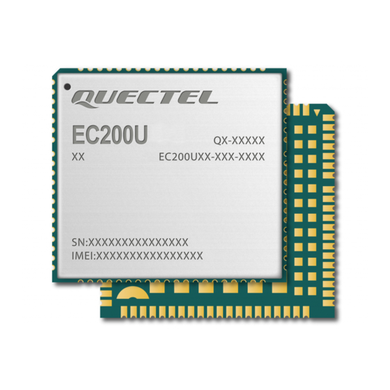
Figure 41: Top & Bottom View of the Module NOTE Images above are for illustration purpose only and may differ from the actual module. For authentic appearance and label, please refer to the module received from Quectel. EC200U_Series_Hardware_Design 86 / 94... -
Page 92: Storage, Manufacturing & Packaging
LTE Standard Module Series Storage, Manufacturing & Packaging 7.1. Storage Conditions The module is provided with vacuum-sealed packaging. MSL of the module is rated as 3. The storage requirements are shown below. Recommended Storage Condition: The temperature should be 23 ± 5 ° C and the relative humidity should be 35–60 %. -
Page 93: Manufacturing And Soldering
LTE Standard Module Series NOTE 1. To avoid blistering, layer separation and other soldering issues, extended exposure of the module to the air is forbidden. 2. Take out the module from the package and put it on high-temperature-resistant fixtures before baking. -
Page 94: Packaging Specifications
PCB or shielding cover, and prevent the coating material from flowing into the module. Due to the complexity of the SMT process, please contact Quectel Technical Supports in advance for any situation that you are not sure about, or any process (e.g. selective soldering, ultrasonic soldering) that is not mentioned in document [4]. -
Page 95: Carrier Tape
LTE Standard Module Series 7.3.1. Carrier Tape Dimension details are as follow: Figure 43: Carrier Tape Dimension Drawing Table 54: Carrier Tape Dimension Table (Unit: mm) 31.5 28.5 20.2 1.75 7.3.2. Plastic Reel Figure 44: Plastic Reel Dimension Drawing EC200U_Series_Hardware_Design 90 / 94... - Page 96 LTE Standard Module Series Table 55: Plastic Reel Dimension Table (Unit: mm) øD1 øD2 44.5 7.3.3. Packaging Process Place the module into the carrier tape and use the cover tape to cover them; then wind the heat-sealed carrier tape to the plastic reel and use the protective tape for protection.
- Page 97 LTE Standard Module Series Appendix References Table 56: Related Documents Document Name [1] Quectel_UMTS<E_EVB_User_Guide [2] Quectel_EC200U&EG915U_Series_AT_Commands_Manual [3] Quectel_RF_Layout_Application_Note [4] Quectel_Module_SMT_User_Guide Table 57: Terms and Abbreviations Abbreviation Description Analog-to-Digital Converter Adaptive Multi-Rate Bits Per Second CHAP Challenge Handshake Authentication Protocol CMUX Connection Multiplexing Coding Scheme Clear to Send...
- Page 98 LTE Standard Module Series Data Terminal Ready Enhanced Full Rate EGSM Enhanced GSM Electromagnetic Interference Electrostatic Discharge Equivalent Series Resistance Evaluation Board Frequency Division Duplex Full Rate File Transfer Protocol FTPS FTP-over-SSL Ground Global System for Mobile Communications Half Rate HTTP Hypertext Transfer Protocol HTTPS...
- Page 99 LTE Standard Module Series Password Authentication Protocol Printed Circuit Board Personal Digital Assistant Protocol Data Unit Paging Frame Point of Sale Point-to-Point Protocol Radio Frequency Red, Green, Blue Smart Media Short Message Service SMTP Simple Mail Transfer Protocol Secure Sockets Layer Transmission Control Protocol Time Division Duplexing UART...
- Page 100 LTE Standard Module Series Minimum High-level Input Voltage Maximum Low-level Input Voltage Minimum Low-level Input Voltage Maximum High-level Output Voltage Minimum High-level Output Voltage Maximum Low-level Output Voltage Minimum Low-level Output Voltage VSWR Voltage Standing Wave Ratio WCDMA Wideband Code Division Multiple Access WLAN Wireless Local Area Network EC200U_Series_Hardware_Design...
Need help?
Do you have a question about the EC200U Series and is the answer not in the manual?
Questions and answers