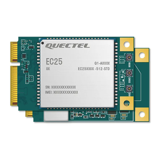
Quectel EC25 Hardware Design
Mini pcie lte module
Hide thumbs
Also See for EC25:
- User manual (71 pages) ,
- Command manual (232 pages) ,
- Reference design (15 pages)

Subscribe to Our Youtube Channel
Related Manuals for Quectel EC25


Summary of Contents for Quectel EC25
- Page 1 EC25 Mini PCIe Hardware Design LTE Module Series Rev. EC25_Mini_PCIe_Hardware_Design_V1.1 Date: 2017-01-24 www.quectel.com...
- Page 2 QUECTEL OFFERS THE INFORMATION AS A SERVICE TO ITS CUSTOMERS. THE INFORMATION PROVIDED IS BASED UPON CUSTOMERS’ REQUIREMENTS. QUECTEL MAKES EVERY EFFORT TO ENSURE THE QUALITY OF THE INFORMATION IT MAKES AVAILABLE. QUECTEL DOES NOT MAKE ANY WARRANTY AS TO THE INFORMATION CONTAINED HEREIN, AND DOES NOT ACCEPT ANY LIABILITY FOR ANY INJURY, LOSS OR DAMAGE OF ANY KIND INCURRED BY USE OF OR RELIANCE UPON THE INFORMATION.
-
Page 3: About The Document
Frank WANG 1. Deleted description of EC25-AUT Mini PCIe in Table 1. 2. Added description of EC25-AU and EC25-J Mini PCIe in Table 1. 3. Updated key features of EC25 Mini PCIe in Lyndon LIU/ 2017-01-24 Table 2. Frank WANG 4. -
Page 4: Table Of Contents
Key Features ........................... 11 2.4. Functional Diagram ......................... 13 Application Interface ......................... 14 3.1. General Description ......................... 14 3.2. EC25 Mini PCIe Interface ......................14 3.2.1. Definition of Interface ..................... 14 3.2.2. Pin Assignment ......................17 3.3. Power Supply ........................... 18 3.4. - Page 5 LTE Module Series EC25 Mini PCIe Hardware Design 5.2. Mechanical Dimensions of EC25 Mini PCIe ................38 5.3. Standard Dimensions of Mini PCI Express ................39 5.4. Packaging Specification ......................40 Appendix References ........................41 EC25_Mini_PCIe_Hardware_Design Confidential / Released 4 / 42...
- Page 6 TABLE 23: CURRENT CONSUMPTION OF EC25-E MINI PCIE ..............34 TABLE 24: CURRENT CONSUMPTION OF EC25-V MINI PCIE ..............37 TABLE 25: GNSS CURRENT CONSUMPTION OF EC25 MINI PCIE SERIES MODULE ....... 37 TABLE 26: RELATED DOCUMENTS ........................ 41 TABLE 27: TERMS AND ABBREVIATIONS ...................... 41...
- Page 7 FIGURE 13: DIMENSIONS OF THE RF CONNECTOR (UNIT: MM) ............... 28 FIGURE 14: MECHANICALS OF U.FL-LP CONNECTORS ................28 FIGURE 15: MECHANICAL DIMENSIONS OF EC25 MINI PCIE (UNIT: MM) ..........38 FIGURE 16: STANDARD DIMENSIONS OF MINI PCI EXPRESS (UNIT: MM) ..........39 FIGURE 17: DIMENSIONS OF THE MINI PCI EXPRESS CONNECTOR (MOLEX 679100002, UNIT: MM)..
-
Page 8: Introduction
EC25 Mini PCIe module. To facilitate its application in different fields, relevant reference design documents are also provided. Associated with application note and user guide of EC25 Mini PCIe module, you can use the module to design and set up mobile applications easily. -
Page 9: Safety Information
The following safety precautions must be observed during all phases of the operation, such as usage, service or repair of any cellular terminal or mobile incorporating EC25 Mini PCIe module. Manufacturers of the cellular terminal should send the following safety information to users and operating personnel, and incorporate these guidelines into all manuals supplied with the product. -
Page 10: Product Concept
Product Concept 2.1. General Description EC25 Mini PCIe module provides data connectivity on LTE-FDD, LTE-TDD, WCDMA and GSM networks with PCI Express Mini Card 1.2 standard interface. It supports embedded operating systems such as WinCE, Linux, Android, etc., and also provides audio, high-speed data transmission and GNSS functionalities for your applications. -
Page 11: Description Of Product Series
LTE Module Series EC25 Mini PCIe Hardware Design 2.2. Description of Product Series The following table shows the product series of EC25 Mini PCIe module. Table 1: Description of EC25 Mini PCIe Product Series Description Support WCDMA: B2/B4/B5 Support LTE-FDD: B2/B4/B12... -
Page 12: Key Features
LTE Module Series EC25 Mini PCIe Hardware Design B2 band on EC25-AU Mini PCIe module does not support receive diversity. 2.3. Key Features The following table describes the detailed features of EC25 Mini PCIe module. Table 2: Key Features of EC25 Mini PCIe... - Page 13 Rx-diversity Support LTE/WCDMA Rx-diversity Gen8C Lite of Qualcomm GNSS Features Protocol: NMEA 0183 Compliant with 3GPP TS 27.007, 27.005 and Quectel enhanced AT AT Commands commands Size: (51.0± 0.1) × (30.0± 0.1) × (4.9± 0.2 mm) Physical Characteristics Weight: approx. 9.8g...
-
Page 14: Functional Diagram
When the temperature returns to normal operating temperature levels, the module is compliant with 3GPP specification again. 2.4. Functional Diagram The following figure shows the block diagram of EC25 Mini PCIe. Boost VBAT... -
Page 15: Application Interface
Control signals Antenna interface 3.2. EC25 Mini PCIe Interface 3.2.1. Definition of Interface The following tables show the pin definition and description of EC25 Mini PCIe on the 52-pin application. Table 3: Definition of I/O Parameters Type Description Bidirectional... - Page 16 LTE Module Series EC25 Mini PCIe Hardware Design Table 4: Description of Pins Mini PCI Express EC25 Mini PCIe Pin No. Description Comment Standard Name Pin Name Output signal can be used WAKE# WAKE# to wake up the host. 3.3Vaux VCC_3V3 3.3V DC supply...
- Page 17 LTE Module Series EC25 Mini PCIe Hardware Design 3.3Vaux RESERVED Reserved Connect to PERp0 UART_RTS UART request to send DTE’s CTS Mini card ground Mini card ground 1.5V Mini card ground Require external SMB_CLK I2C_SCL I2C serial clock pull-up to 1.8V.
-
Page 18: Pin Assignment
Keep all NC, reserved and unused pins unconnected. “*” means the digital audio (PCM) function is only supported on Telematics version. 3.2.2. Pin Assignment The following figure shows the pin assignment of EC25 Mini PCIe module. The top side contains EC25 module and antenna connectors. PIN1... -
Page 19: Power Supply
37, 40, 43, 50 The typical supply voltage of EC25 Mini PCIe is 3.3V. In the 2G networks, the input peak current may reach to 2.7A during the transmitting time. Therefore, the power supply must be able to provide enough current, and a bypass capacitor of no less than 470µF with low ESR should be used to prevent the... -
Page 20: Usim Card Interface
USIM data signal USIM_CLK 1.8V/3.0V USIM clock signal USIM_RST 1.8V/3.0V USIM reset signal EC25 Mini PCIe supports 1.8V and 3.0V USIM cards. The following figure shows a reference design for a 6-pin USIM card connector. USIM_VDD 100nF Module USIM Card Connector USIM_VDD... -
Page 21: Usb Interface
USB differential data (+) EC25 Mini PCIe is compliant with USB 2.0 specification. It can only be used as a slave device. Meanwhile, it supports high speed (480Mbps) mode and full speed (12Mbps) mode. The USB interface is used for AT command communication, data transmission, GNSS NMEA output, software debugging, firmware upgrade and voice over USB*. -
Page 22: Uart Interface
Keep traces of USB data test points short to avoid noise coupled on USB data lines. If possible, reserve a 0R resistor on these two lines. NOTES There are three preconditions when enabling EC25 Mini PCIe to enter into the sleep mode: Execute AT+QSCLK=1 command to enable the sleep mode. Please refer to document [2] for details. -
Page 23: Pcm And I2C Interfaces
I2C_SDA 1.8V pull-up to 1.8V. EC25 Mini PCIe provides one PCM digital interface, which supports 8-bit A-law* and μ-law*, and also supports 16-bit linear data formats and the following modes: Primary mode (short frame synchronization, works as either master or slave) ... - Page 24 LTE Module Series EC25 Mini PCIe Hardware Design In primary mode, the data is sampled on the falling edge of the PCM_CLK and transmitted on the rising edge. The PCM_SYNC falling edge represents the MSB. In this mode, PCM_CLK supports 128, 256, 512, 1024 and 2048kHz for different speed codecs.
-
Page 25: Control Signals
Clock and mode can be configured by AT command, and the default configuration is master mode using short frame synchronization format with 2048kHz PCM_CLK and 8kHz PCM_SYNC. In addition, EC25 Mini PCIe’s firmware has integrated the configuration on some PCM codec’s application with I2C interface. -
Page 26: Ri Signal
The DTR signal supports sleep control function. Driving it to low level will wake up the module. 3.8.3. W_DISABLE# Signal EC25 Mini PCIe provides W_DISABLE# signal to disable wireless communications through hardware operation. The following table shows the radio operational states of the module. Please refer to document [2] for related AT commands. -
Page 27: Led_Wwan# Signal
3.8.5. LED_WWAN# Signal The LED_WWAN# signal of EC25 Mini PCIe is used to indicate the network status of the module, which can absorb the current up to 40mA. According to the following circuit, in order to reduce the current of the LED, a resistor must be placed in series with the LED. -
Page 28: Wake# Signal
Figure 12: WAKE# Behavior 3.9. Antenna Interfaces EC25 Mini PCIe antenna interfaces include a main antenna interface, an Rx-diversity antenna interface and a GNSS antenna interface. And Rx-diversity function is enabled by default. The following table shows the requirement on main antenna, Rx-diversity antenna and GNSS antenna. - Page 29 LTE Module Series EC25 Mini PCIe Hardware Design The following figure shows the overall sizes of RF connector. Figure 13: Dimensions of the RF Connector (Unit: mm) U.FL-LP serial connectors listed in the following figure can be used to match the RF connector.
-
Page 30: Electrical And Radio Characteristics
ESD characteristics 4.2. Power Supply Requirements The input voltage of EC25 Mini PCIe is 3.3V± 9%, as specified by PCI Express Mini CEM Specifications 1.2. The following table shows the power supply requirements of EC25 Mini PCIe. Table 14: Power Supply Requirements... -
Page 31: I/O Requirements
2. The maximum voltage value of V for PERST# signal and W_DISABLE# signal is 0.5V. 4.4. RF Characteristics The following tables show the conducted RF output power and receiving sensitivity of EC25 Mini PCIe module. Table 16: EC25 Mini PCIe Conducted RF Output Power Frequency Max. - Page 32 LTE Module Series EC25 Mini PCIe Hardware Design LTE-TDD bands 23dBm± 2dB <-44dBm Table 17: EC25-A Mini PCIe Conducted RF Receiving Sensitivity Frequency Primary Diversity SIMO 3GPP (SIMO) WCDMA B2 -110.0dBm -104.7dBm WCDMA B4 -110.0dBm -106.7dBm WCDMA B5 -110.5dBm -104.7dBm LTE FDD B2 (10M) -98.0dBm...
-
Page 33: Gnss Receiver
-93.3dBm 4.5. GNSS Receiver EC25 Mini PCIe integrates a GNSS receiver that supports IZat Gen 8C Lite of Qualcomm (GPS, GLONASS, BeiDou, Galileo, QZSS). Meanwhile, it supports Qualcomm gpsOneXTRA technology (one kind of A-GNSS). This technology will download XTRA file from the internet server to enhance the TTFF. -
Page 34: Esd Characteristics
NMEA-0183 protocol and output NMEA messages with 1Hz via USB NMEA interface. EC25 Mini PCIe GNSS engine is switched off by default. You must switch on it by AT command. Please refer to document [3] for more details about GNSS engine technology and configurations. A passive antenna should be used for the GNSS engine. - Page 35 WCDMA B2 @23.59dBm 861.0 WCDMA WCDMA B4 @23.47dBm 812.0 voice call WCDMA B5 @23.46dBm 683.0 Table 23: Current Consumption of EC25-E Mini PCIe Parameter Description Conditions Typ. Unit AT+CFUN=0 (USB disconnected) GSM DRX=2 (USB disconnected) GSM DRX=9 (USB disconnected) Sleep state...
- Page 36 LTE Module Series EC25 Mini PCIe Hardware Design LTE-FDD PF=128 (USB disconnected) LTE-TDD PF=64 (USB disconnected) LTE-TDD PF=128 (USB disconnected) GSM DRX=5 (USB disconnected) 30.0 GSM DRX=5 (USB connected) 43.0 WCDMA PF=64 (USB disconnected) 31.0 WCDMA PF=64 (USB connected) 45.0...
- Page 37 LTE Module Series EC25 Mini PCIe Hardware Design DCS1800 2DL/3UL @25.97dBm 440.0 DCS1800 1DL/4UL @25.82dBm 553.0 WCDMA B1 HSDPA @22.49dBm 798.0 WCDMA B1 HSUPA @21.87dBm 788.0 WCDMA data WCDMA B5 HSDPA @22.66dBm 781.0 transfer WCDMA B5 HSUPA @21.99dBm 770.0 (GNSS OFF) WCDMA B8 HSDPA @22.23dBm...
- Page 38 LTE-FDD PF=64 (USB connected) 42.0 LTE data LTE-FDD B4 @23.3dBm 873.0 transfer LTE-FDD B13 @22.13dBm 638.0 (GNSS OFF) Table 25: GNSS Current Consumption of EC25 Mini PCIe Series Module Parameter Description Conditions Typ. Unit Cold start @Passive Antenna 75.0 Searching (AT+CFUN=0) Lost state @Passive Antenna 74.0...
-
Page 39: Dimensions And Packaging
EC25 Mini PCIe Hardware Design Dimensions and Packaging 5.1. General Description This chapter mainly describes mechanical dimensions as well as packaging specification of EC25 Mini PCIe module. 5.2. Mechanical Dimensions of EC25 Mini PCIe Figure 15: Mechanical Dimensions of EC25 Mini PCIe (Unit: mm) - Page 40 LTE Module Series EC25 Mini PCIe Hardware Design 5.3. Standard Dimensions of Mini PCI Express The following figure shows the standard dimensions of Mini PCI Express. Please refer to document [1] for detailed A and B. Figure 16: Standard Dimensions of Mini PCI Express (Unit: mm)
- Page 41 Figure 17: Dimensions of the Mini PCI Express Connector (Molex 679100002, Unit: mm) 5.4. Packaging Specification The EC25 Mini PCIe is packaged in a tray. Each tray contains 10pcs of modules. The smallest package of EC25 Mini PCIe contains 100pcs.
- Page 42 Table 26: Related Documents Document Name Remark PCI Express Mini Card Electromechanical Mini PCI Express Specification Specification Revision 1.2 Quectel_EC25&EC21_AT_Commands_Manual EC25 and EC21 AT Commands Manual Quectel_EC25&EC21_GNSS_AT_Commands_ EC25 and EC21 GNSS AT Commands Manual Manual Table 27: Terms and Abbreviations Abbreviation...
- Page 43 LTE Module Series EC25 Mini PCIe Hardware Design GNSS Global Navigation Satellite System Global Positioning System Global System for Mobile Communications Half Rate kbps Kilo Bits Per Second Light Emitting Diode Long-Term Evolution Mbps Million Bits Per Second Mobile Equipment (Module)
Need help?
Do you have a question about the EC25 and is the answer not in the manual?
Questions and answers