Table of Contents
Advertisement
Quick Links
Advertisement
Table of Contents

Related Manuals for Sony TRIMASTER EL BVM-E171


Summary of Contents for Sony TRIMASTER EL BVM-E171
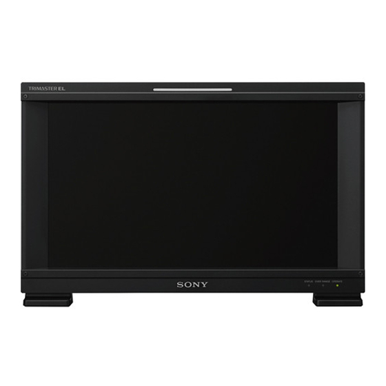
- Page 1 PROFESSIONAL VIDEO MONITOR BVM-E171 SERVICE MANUAL 1st Edition (Revised 1)
- Page 2 警告 このマニュアルは,サービス専用です。 お客様が,このマニュアルに記載された設置や保守,点検,修理などを行うと感電や火災, 人身事故につながることがあります。 危険をさけるため,サービストレーニングを受けた技術者のみご使用ください。 WARNING This manual is intended for qualified service personnel only. To reduce the risk of electric shock, fire or injury, do not perform any servicing other than that contained in the operating instructions unless you are qualified to do so. Refer all servicing to qualified service personnel.
- Page 3 警告 本機をラックに設置するとき 熱の適切な排気・発散を得るために,ラックと本機の 本機は電源スイッチを備えていません。 間には,以下の空間を確保してください。 万一,異常が起きた際に,お客様が電源をきることが ・上下に 1U(4.4 cm)以上 できるように,設置の際には,機器近くの固定配線内 ・左右に 1.0 cm 以上 に専用遮断装置を設けるか,機器使用中に,容易に抜 き差しできるコンセントに電源プラグを接続してくだ さい。 Attention-when the product is installed in Rack: WARNING 1. Prevention against overloading of branch circuit This unit has no power switch. When installing the unit, incorporate a readily accessible When this product is installed in a rack and is disconnect device in the fixed wiring, or connect the supplied power from an outlet on the rack, please...
- Page 4 注意 感電の危険があります。 本製品の一次回路のヒューズが,中性線側に接続さ れる可能性があります。 修理時の感電を防ぐため,本機を主電源から切り離 してください。 CAUTION RISK OF ELECTRIC SHOCK The fuse of the primary circuit of this product may be connected on the neutral wire side. Disconnect the unit from the power supply to prevent electric shock when repairing. ATTENTION RISQUE D’ÉLECTROCUTION Le fusible du circuit primaire de ce produit peut être...
-
Page 5: Table Of Contents
Table of Contents Manual Structure Purpose of this manual........................5 Related manuals. - Page 6 3-3-6. Abnormal Device..................... .3-10 3-3-7.
- Page 7 6-5. Restore the Factory Default Settings..................6-5 6-6.
-
Page 9: Purpose Of This Manual
Manual Structure Purpose of this manual This manual is the Service Manual of the Professional Video Monitor BVM-E171. This manual describes the information on the premise of providing the block level service (service overview, periodic replacement parts and cleaning, troubleshooting, replacement of board and main parts, upgrade, maintenance menu, circuit description, spare parts, block diagrams, frame wiring). -
Page 11: Service Overview
Section 1 Service Overview 1-1. Precaution for Transporting When transporting this unit, use the packaging materials supplied with this unit in order to prevent damage due to the vibration and shock. • Keep the packaging materials removed when this unit is delivered and installed. Do not discard them. •... -
Page 12: Location Of Main Parts
1-2. Location of Main Parts DC fan BA board YA board YD board G board BC board ST1 board PT1 board YB board BVM-E171... -
Page 13: Conductive Cushion
1-3. Conductive Cushion Put a monitor on the conductive cushion as shown in the figure below. This prevents the panel or bezel assembly from being damaged. Use a conductive material to prevent static electricity. Illustration in this manual A conductive cushion is not described in the illustration of replacement procedure. Monitor Upper side Conductive cushion... -
Page 14: Preparation For Service
Preparation for Service 1-4-1. Preparing Upgrade Data To upgrade the firmware, the upgrade data is necessary. For obtaining the upgrade data, contact your local Sony Sales Office/Service Center. Equipment required • Personal computer (PC) OS: Windows 7 or Windows8, Windows8.1 •... -
Page 15: Folder Structure Of Upgrading Data
1-4-2. Folder Structure of Upgrading Data /MSSONY /MONITOR /BKM /UPDATES /SOFT /BKM_17R /bin /check_data /data.com CONTENTS checksum_soft.bat /KERNEL /BKM_17R /check_data binary_size checksum_kernel.bat version vxWorks_rom.bin /BVM_E1 /UPDATES /SOFT /BVM_E251 /bin /check_data /data.com /data.adj CONTENTS checksum_soft.bat /SOFT /BKM_E171 /bin /check_data /data.com /data.adj CONTENTS checksum_soft.bat /KERNEL... -
Page 16: Check Of Usb Flash Drive Data
1-4-3. Check of USB Flash Drive Data After copying the version upgrade data from PC to USB flash drive, check if the data is correctly copied by using the checksum. Equipment required • Personal computer (PC) OS: Windows 7 or Windows8, Windows8.1 •... -
Page 17: Pc Setting
If data is not stored normally [Error] is displayed. 1-4-4. PC Setting When upgrading the software, kernel, and FPGAs or performing process after replacing the each board or OLED module, make the PC setting. Equipment required • Personal computer (PC) OS: Windows 7 or Windows8, Windows8.1 •... -
Page 18: Host (Ftp) Setting
Select [Internet Protocol Version 4 (TCP/IPv4)] and click the [Properties] button. Enter “192.168.0.10” in the [IP address] field, enter “255.255.255.0” in the [Subnet mask] field, and then click the [OK] button. Click [OK]. The Local Area Connection Properties screen closes. 1-4-5. - Page 19 English: http://en.osdn.jp/projects/ffftp/ Equipment Required • Personal computer (PC) OS: Windows 7 or Windows8, Windows8.1 • LAN cable (cross cable) • FTP client software (FFFTP) Procedure Run the FFFTP. BVM-E171...
- Page 20 • Do not use full path to access files: Do not select this checkbox. • Permissions Change Command: SITE CHMOD • Host Type: ShibaSoku WL • NLST Filename: -alL Click [OK]. For username and password/phrase, contact your local Sony Sales Office/Service Center. 1-10 BVM-E171...
-
Page 21: Connecting Commands From The Pc
1-4-6. Connecting Commands from the PC The terminal software TeraTerm (open source software) is used in this section. Refer to the following websites about TeraTerm. Japanese: http://ttssh2.sourceforge.jp/index.html.ja English: http://ttssh2.sourceforge.jp/index.html.en Note Commands for the TeraTerm are two types (MR6 and DgTerm). TCP port, user name, and password are different for MR6 commands and DgTerm commands. -
Page 22: How To Check The Versions
Log in to the unit. For user name and password, contact your local Sony Sales Office/Service Center. (1) Enter user name and press the Enter key. [pass:] appears. (2) Enter password and press the Enter key. [>] appears to allow you to enter a command. -
Page 23: Circuit Protection Parts
1-5. Circuit Protection Parts 1-5-1. Fuses WARNING Fuses are essential parts for safe operation. Be sure to use the parts specified in this manual. Replacing a fuse with an unspecified one may cause fire or electric shock. CAUTION Replacing any fuse is replaced while power is supplied to the unit may cause electric shock. Before replacing any fuse , turn off the POWER switch and also disconnect the cable from the DC IN connector. - Page 24 Board Name Ref. No. Part Name and Rating Part No. F6200 FUSE, MICRO (1608) 1.4 A/32 V 1-576-406-31 F6201 FUSE, MICRO (1608) 1.4 A/32 V 1-576-406-31 F7000 MICRO FUSE-LINK (1608 TYPE) 4 A/24 V 1-576-958-31 F7001 MICRO FUSE-LINK (1608 TYPE) 2 A/32 V 1-576-415-31 F7002 MICRO FUSE-LINK (1608 TYPE) 2.5 A/32 V...
-
Page 25: Flexible Flat Cable And Fine-Wire Coaxial Cable
1-6. Flexible Flat Cable and Fine-Wire Coaxial Cable 1-6-1. Disconnecting/Connecting Flexible Flat Cable Note • Be very careful not to fold flexible flat cable. Life of flexible flat cable will be significantly shortened if it is folded. • Each flexible flat cable has conductor side and insulated side. If the flexible flat cable is connected in the wrong orientation of the conductor side and the insulated side, the circuit will not function. -
Page 26: Disconnecting/Connecting The Fine-Wire Coaxial Cable
Guide Guide Flexible flat cable Guide Guide 1-6-2. Disconnecting/Connecting the Fine-Wire Coaxial Cable Note • Be very careful when handling the fine-wire coaxial cable so that fine wires are not disconnected. • When disconnecting the fine-wire coaxial cable, be sure to hold the connector. Do not attempt to pull the cable. •... -
Page 27: Lead-Free Solder
1-7. Lead-free Solder All boards mounted in this unit use lead-free solder. Be sure to use lead-free solder when repairing the boards of this unit. A lead free mark (LF) indicating that the solder contains no lead is printed on each board. (Caution: Some printed circuit boards may not come printed with the lead free mark due to their particular size.) : LEAD FREE MARK Note... -
Page 29: Periodic Replacement Parts And Cleaning
This section indicates the replacement period of parts when this unit is used at an operating temperature of 25 ℃. The replacement period of each part is changed according to the environment and conditions of use. Part name Sony Part No. Number of pieces Replacement period... -
Page 30: Cleaning
2-2. Cleaning Clean the dust near a panel module, inlet port, or fans periodically. It is recommended to clean the dust once a year. An OVER RANGE indicator blinks in amber when luminance decreases to protect the panel during increase in temperature. -
Page 31: Troubleshooting
Section 3 Troubleshooting 3-1. Diagnosis by Indicators Indicators on the front panel of the unit allow you to diagnose errors. While the unit is working normally, only the OPERATE indicator lights green. When an error or alarm occurs in the unit, indicators light or blink as follows. Error indication STATUS indicator OVER RANGE indi-... -
Page 32: Indicators Are Lit Normally
3-2. Indicators Are Lit Normally 3-2-1. No Video or OSD Is Displayed on the Panel Factor Remedy Failure of the panel power line (VGMA, Check whether the fuses (F8702, F8703) are blown. VDD_DRV) on the BC board If any of these fuses is blown, replace IC8700. VGMA 15.5V VDD_GMA... - Page 33 AT3_REC1_SDI_SDIN R2408 REC1_REC2_SDI_SDOUT AT3_REC_SDI_SCLK C2426 3G-SDI INPUT1 AT3_REC_SDI_CS_X X2400 27MHz +3.3V_OP_D_A_SDI1 R2414 C2403 0.01u R2415 C2427 1/16W C2404 0.047u C2405 C2428 0.22u C2420 4.7u VEE_DDO0 C2428 0.01u 6.3V CP_CAP VCC_DDO0 1608 1608 IC2401 1005 EQ1_SDOP GS2965-INTE3 DDI0 DDO0 3G-SDI_IN1_SDOP R2401 DDO0 3G-SDI_IN1_SDOM 3G-SDI...
-
Page 34: Sdi Signal Is Not Displayed
REC1_REC2_SDI_SDOUT R2428 REC2_AT3_SDI_SDOUT AT3_REC_SDI_SCLK C2449 3G-SDI INPUT2 AT3_REC_SDI_CS_X X2401 50V 27MHz +3.3V_OP_D_A_SDI2 C2436 R2434 0.01u R2435 C2450 1/16W C2437 0.047u C2451 C2438 C2445 4.7u 0.22u VEE_DDO0 0.01u 6.3V C2451 CP_CAP VCC_DDO0 1608 1608 IC2403 1005 EQ2_SDOP GS2965-INTE3 DDI0 DDO0 3G-SDI_IN2_SDOP R2421 DDO0 3G-SDI_IN2_SDOM... -
Page 35: The Controller Cannot Be Connected
3-2-5. The Controller Cannot Be Connected Check the following: • Check whether cables are connected correctly. • Check whether the NETWORK switches on the unit and the controller are set correctly. (Refer to the operating instructions.) • Check whether network settings (including IP address) are made correctly. (Refer to the operating instructions.) 3-2-6. -
Page 36: Indicators Are Lit Abnormally Or Blinking
3-3. Indicators Are Lit Abnormally or Blinking 3-3-1. Abnormal Panel Power Source Schematic diagram of panel power Flow of current F9000 FUSE D9004 IC9000 Q9002 R9063 L9000 ON/OFF DS-H Q9003 D9005 CLOCK Controller F9001 C9034/C9038 LTC3857 FUSE D9006 PGOOD Q9005 R9064 L9001 Panel... -
Page 37: Abnormal Panel Temperature
When VDDDS is output for about 48 ms but it stops again Factor Remedy An abnormality of the power on the Check whether the fuses (F9002, F9003, F9004, F9005) are blown. If any of VCATH side is considered. these fuses is blown, replace defective parts. •... -
Page 38: Abnormal External Temperature Sensor
• Check the luminance setting. In most cases, the luminance cannot be lowered due to the detection after the process of the lowering of luminance. However, if there is any possibility to lower the luminance, lower it. If the above remedy cannot be implemented, lower the panel temperature in such a way as to cool it forcibly by using an external cooling device separately. -
Page 39: Abnormal Fan
Upgrading the FPGA using the controller (“5-1. Upgrade Method”) is enabled. Remedy Check the BA board status according to the following flowchart. Power on Always lit Is D1000 lit? Lights for about one second and then goes out. (Normal state) Are RB2501, R2517, BA board R2518, R2500, R2507,... -
Page 40: Abnormal Device
• For the external temperature and panel temperature, refer to “6-10. Displaying Panel Temperature and Room Temperature”. Unit status at an error Only a notification (front indicator) of abnormal state Remedy Check the following items of the applicable fan. • Check the foreign substances in the fan. •... -
Page 41: Dynamic Range Over
Remedy • Check the installation environment. If the environment temperature is higher than the recommended temperature, lower it. If there is something that blocks the fan exhaust outlet or ventilation outlet in the rear portion of this unit, remove Ensure the space around this unit for ventilation. •... -
Page 42: Other Errors
3-4. Other Errors 3-4-1. The Unit Cannot Be Turned On The unit cannot be turned on. (OPERATE indicator does not light.) Is the power cable Connect the power cord correctly. connected correctly? Is the fuse (F6000) Replace the fuse (F6000). on the G board drown? Are the fuses Replace the fuses... - Page 43 Remedy Check the BA board status according to the following flowchart. (For checking the power system, refer to “7-2-2. Power Systems”.) Power on Is the D0400 lit? Abnormal power system Never lights Always lights Blinks just for a moment .Check whether peripheral .Check independent Is +3.3V_BA parts of the IC0301 are...
-
Page 45: Replacement Of Board And Main Parts
Section 4 Replacement of Board and Main Parts 4-1. Guide of Removal Viewing the schematic diagram: Start of removal : Removal of parts : Replacement of parts Rear cover VESA bracket Power Bottom cabinet assembly assembly block assembly G board YD board ST1 board BA board... -
Page 46: Tightening Torque
4-2. Tightening Torque Tighten the each screw with the torque below. • B3 x 5 (for BA cover block): 0.40 ±0.10 N·m • B3 x 5 (for excluding BA cover block): 0.80 ±0.10 N·m • B3 x 6: 0.80 ±0.10 N·m •... -
Page 47: Rear Cover Assembly
4-3. Rear Cover Assembly Procedure Remove the two screws (B4 x 6), then remove the handle. Remove the 13 screws (B4 x 6) and four screws (PSW4 x 10), then remove the rear cover assembly. Remove the two screws (PSW4 x 8), then remove the two front leg assemblies. B4 x 6 Handle B4 x 6... -
Page 48: Power Block
4-4. Power Block Preparation Remove the rear cover assembly. (Refer to “4-3. Rear Cover Assembly”.) Remove the VESA bracket assembly. (Refer to “4-5. Bottom Cabinet Assembly”.) Procedure Remove the screw, then remove the power block. Disconnect the four harnesses from the connectors (CN3000, CN3001, CN6000 and CN6003) on the G board. Open the two clampers, then remove the four harnesses. - Page 49 Remove the four hooks, then remove the connector assembly with AC switch. 3 x 12 Plug holder (A) Connector assembly with AC switch AC inlet Hooks RK2.6 x 6 Hooks DC connector AC bracket Ground wire (green) 4 x 8 4 x 8 Clamper Ground wire...
-
Page 50: Bottom Cabinet Assembly
4-5. Bottom Cabinet Assembly Preparation Remove the rear cover assembly. (Refer to “4-3. Rear Cover Assembly”.) Remove the power block. (Refer to “4-4. Power Block”.) Procedure Remove the four screws (PSW3 x 6), then remove the VESA bracket assembly. Remove the harness from the clamper. Disconnect the harness from the connector (CN300) on the ST1 board. -
Page 51: St1 Board
4-6. ST1 Board Preparation Remove the rear cover assembly. (Refer to “4-3. Rear Cover Assembly”.) Remove the VESA bracket assembly. (Refer to “4-5. Bottom Cabinet Assembly”.) Procedure Disconnect the harness from the connector (CN300) on the ST1 board. Remove the screw, then remove the ST1 board and insulating plate (ST). Insulating plate (ST) ST1 board Harness... -
Page 52: Yd Board
4-7. YD Board Preparation Remove the rear cover assembly. (Refer to “4-3. Rear Cover Assembly”.) Procedure Disconnect the harness from the connector (CN100) on the YD board. Remove the two screws, then remove the YD board. 3 x 6 CN100 Harness YD board Clamper... -
Page 53: G Board
4-8. G Board Preparation Remove the rear cover assembly. (Refer to “4-3. Rear Cover Assembly”.) Remove the power block. (Refer to “4-4. Power Block”.) Remove the bottom cabinet assembly. (Refer to “4-5. Bottom Cabinet Assembly”.) Procedure Disconnect the four harnesses from the connectors (CN7000 to CN7003) on the G board. Remove the screw, then remove the cable clamp. -
Page 54: Ba Board
4-9. BA Board Note When replacing the BA board, refer to “4-16-2. After Replacing or Repairing the BA Board and FLASH (IC1203)”. Preparation Remove the rear cover assembly. (Refer to “4-3. Rear Cover Assembly”.) Remove the power block. (Refer to “4-4. - Page 55 Remove the four screws, then remove the BA board. 3 x 6 Heat sink (BA) Radiation sheet (BA) Radiation sheets (S) 3 x 6 BA board Upper side Note When installing the BA board, tighten the four screws in the order from (a) to (d). 10.
-
Page 56: Dc Fan
4-10. DC Fan Preparation Remove the rear cover assembly. (Refer to “4-3. Rear Cover Assembly”.) Remove the power block. (Refer to “4-4. Power Block”.) Remove the bottom cabinet assembly. (Refer to “4-5. Bottom Cabinet Assembly”.) Remove the BA board. (Refer to “4-9. -
Page 57: Oled Module Assembly And Bezel Assembly
4-11. OLED Module Assembly and Bezel Assembly Note When replacing the OLED module assembly, refer to “4-16-1. After Replacing the OLED Module”. Preparation Remove the rear cover assembly. (Refer to “4-3. Rear Cover Assembly”.) Remove the power block. (Refer to “4-4. - Page 58 Remove the six screws (B3 x 5), then remove the OLED module assembly. Harness Harness Nylon rivets 3 x 6 Insulating plate Main frame assembly CN7100 Harness B3 x 5 Route the harness to be connected to the BC board B3 x 5 connector (CN3000) on the BC board as shown in the illustration.
-
Page 59: Ya Board
4-12. YA Board Preparation Remove the rear cover assembly. (Refer to “4-3. Rear Cover Assembly”.) Remove the power block. (Refer to “4-4. Power Block”.) Remove the bottom cabinet assembly. (Refer to “4-5. Bottom Cabinet Assembly”.) Remove the G board. (Refer to “4-8. -
Page 60: Yb Board
4-13. YB Board Preparation Remove the rear cover assembly. (Refer to “4-3. Rear Cover Assembly”.) Remove the power block. (Refer to “4-4. Power Block”.) Remove the bottom cabinet assembly. (Refer to “4-5. Bottom Cabinet Assembly”.) Remove the G board. (Refer to “4-8. -
Page 61: Bc Board
4-14. BC Board The BC board is not available as repair parts. When the BC board is damaged, replace the OLED module assembly. Preparation Remove the rear cover assembly. (Refer to “4-3. Rear Cover Assembly”.) Remove the power block. (Refer to “4-4. - Page 62 Remove the five screws, then remove the BC board. Harnesses Harness CN9005 CN9103 Flexible flat cables CN9003 CN9102 3 x 6 Flexible flat CN9007 cable Harness CN9001 CN9006 CN9000 CN9002 3 x 6 CN9101 Harness CN9100 Cable clamp Harness CN3004 BC board Flexible flat cable Upper side...
-
Page 63: Pt1 Board
4-15. PT1 Board Preparation Remove the rear cover assembly. (Refer to “4-3. Rear Cover Assembly”.) Remove the power block. (Refer to “4-4. Power Block”.) Remove the bottom cabinet assembly. (Refer to “4-5. Bottom Cabinet Assembly”.) Remove the G board. (Refer to “4-8. -
Page 64: Procedures After Replacing The Boards And Parts
4-16. Procedures after Replacing the Boards and Parts After any of the following boards or parts is replaced, perform the procedure in this section to take necessary actions. • OLED module assembly (Refer to “4-16-1. After Replacing the OLED Module”.) •... - Page 65 Set the NETWORK switch of the unit and controller to “PEER TO PEER”. Setup the PC. (Refer to “1-4-4. PC Setting”.) Setup the host. (Refer to “1-4-5. Host (FTP) Setting”.) For [Local initial folder], specify the folder that contains the model name file and the serial number file. Procedure Turn on the unit.
-
Page 66: After Replacing Or Repairing The Ba Board And Flash (Ic1203)
4-16-2. After Replacing or Repairing the BA Board and FLASH (IC1203) After the BA board and FLASH (IC1203) has been repaired or replaced, perform the following work as required. • FPGA upgrade (Refer to “5-1-4. Procedure for Upgrading the FPGA of the Unit”.) •... -
Page 67: Upgrade
First of all, upgrade the software to V1.01 which is the bridge software, and then it is necessary to upgrade it to V1.1. As for the upgrade to the bridge software (V1.01), contact to your local Sony's service office. • When upgrading the software to V1.1, be sure to upgrade both the software and FPGA. -
Page 68: Kernel Upgrade
Select [Software Upgrade]. About 10 seconds later, a message to check old and new software versions and the upgrade execution status appears. Example of display Monitor software will be upgraded and monitor will restart. Are you sure ? Check old and new software versions, and then press the Enter key. Software upgrade starts. -
Page 69: Procedure For Upgrading The Fpga Of The Unit
Check old and new kernel versions, and then press the Enter key. Software upgrade starts. When software upgrade starts, “In progress ■” appears and “■” blinks. Blinking “■” stops during upgrade in some cases, but upgrade is going normally. When the upgrade has been completed, the display disappears and the system restarts. Select [Monitor Upgrade] from the [System Configuration] menu. -
Page 70: Fpga_Core Upgrade
• Version 15.2 or later version of the writing software (Quartus II programmer) may not run normally. In that case, use version 15.1 or older. • For obtaining the upgrade data, contact your local Sony Sales Office/Service Center. Preparation Install the writing software on PC. - Page 71 File select window is displayed. Note If “CFI_32Mb” is not displayed, CPLD_CORE (IC4000) has not been written correctly. For the CPLD_CORE (IC4000) writing method, contact your local Sony Sales Office/Service Center. Select the upgrade file (xxx.pof). The selected file is registered.
-
Page 72: Fpga (Ic1000) Upgrade
Select the checkboxes in the Program/Configure column and click [Start]. Upgrade start. 10. [Progress:] at the upper right of the screen becomes 100% and “Successfully performed operation (s)” appears in the Message field, close the writing software. 11. Turn off the unit and disconnect the PC, service harness, and USB blaster cable. 12. - Page 73 Connect the devices in use as shown in the figure below. USB flash drive BKM-17R Switching HUB LAN cable 12V DC LAN cable LAN cable Set the NETWORK switch of the unit and controller to “PEER TO PEER”. Setup the PC. (Refer to “1-4-4.
- Page 74 Input the “upgrade_fpga_dummy_ui”. “OK” appears and FPGA upgrade starts. • FPGA upgrade takes about 15 minutes. • Upon completion of upgrade, the unit reboots automatically. BVM-E171...
-
Page 75: Recovery From Upgrade Failure
5-2. Recovery from Upgrade Failure 5-2-1. Recovery from Software Upgrade Failure When any of the following problems occurs during software upgrade, upload the upgrade file manually to restore the monitor or the controller. This unit • “Procedure failure” appeared at the bottom of the menu window during upgrade and no video signal is displayed and menu operation from the controller is disabled even after power is turned off and on. - Page 76 Procedure Connect the equipment required as shown below. USB flash drive BKM-17R Switching HUB LAN cable 12V DC LAN cable LAN cable Set the NETWORK switch of the controller and the monitor to PEER TO PEER. Login to PC. Setup the PC. (Refer to “1-4-4.
- Page 77 Connect to the PC. • This unit (1) Remove the parts as BC board is visible. (Refer to “4-11. OLED Module Assembly and Bezel Assembly”.) (2) Set switch 1 of the DIP switch (S3100) on the BC board to ON. (3) Install the YD board by reversing the steps of removal.
-
Page 78: Recovery Procedure When Upgrading The Unit's Kernel Or Fpga Failed
Software data writing procedure Note To write software data, the kernel must be upgraded to the following version. • This unit: Version 1.03 • Controller: Version 3.30 Before writing software data, change the kernel version. (Refer to “5-1-3. Kernel Upgrade”.) Activate FFFTP and set the host. - Page 79 Preparation Remove the parts as BC board is visible. (Refer to “4-11. OLED Module Assembly and Bezel Assembly”.) Set switch 1 of the DIP switch (S3100) on the BC board to ON. Install the YD board by reversing the steps of removal. Connect the PC to the monitor with an RS-232C cable.
-
Page 80: Recovery Procedure When Upgrading The Controller's Kernel Failed
Click [Browse] and set the kernel data to be written. FPGA data: FPGA.rbf Click [Download]. Start writing. Note When a message “all process succeeded” appears, data writing has been completed. Turn off the monitor. Disconnect the RC-232C cable. 10. Set switch 1 of the DIP switch (S3100) on the BC board to OFF. 5-2-3. - Page 81 Kernel data writing procedure Turn off the controller. (Disconnect the power cable from the DC plug.) Turn on the controller. (Connect the power cable to the DC plug.) Setup BVM_HAB_TOOL. Select “Image File” in the [File type] field. On the [Com port] tab window, set the PC’s COM port to be used. Click [Browse] and set the kernel data to be written.
-
Page 83: Maintenance Menu
Section 6 Maintenance Menu 6-1. Display and Operation Button of Maintenance Menu 6-1-1. Explanation of Operation Button Operate the Maintenance Menu by using the button on the controller (BKM-17R, option). The same operation is possible by BKM-16R. For details of buttons of BKM-16R, refer to the BKM-16R operation manual. -
Page 84: Display Method (Maintenance Menu Screen)
Press the MENU button of the controller. Main menu is displayed. Select [Maintenance] of [System Configuration]. The following screen is displayed. Enter password and press the Enter button. Note For password, contact your local Sony Sales Office/Service Center. Maintenance Menu screen is displayed. BVM-E171... -
Page 85: Items Of Maintenance Menu
6-3. Items of Maintenance Menu Maintenance Menu comprises the following items. Big item Middle item Functions Maintenance Low Latency Setting the Low Latency (system delay) mode Restore Factory Set All Restore the factory default settings Restore System Data Storing or loading system data Restore Color Temp Data (Unselectable) Color Temp Offset... -
Page 86: Setting The Low Latency (System Delay) Mode
6-4. Setting the Low Latency (System Delay) Mode Set the Low Latency (system delay) mode when the signal system is in the HDMI signal input with 1080/24P, 1080/25P or 1080/30P. Procedure Select [Low Latency] of Maintenance Menu and press the Enter button. The following screen is displayed. -
Page 87: Restore The Factory Default Settings
6-5. Restore the Factory Default Settings All set values of the monitor are restored to the factory default setting. Procedure Select [Restore Factory Set All] of Maintenance Menu and press the ENTER button. The following screen is displayed. Press the ENTER button. BVM-E171... -
Page 88: Storing Or Loading System Data
6-6. Storing or Loading System Data System data (adjustment data and setting data) of the unit can be stored or loaded. Procedure Connect the USB flash drive to the USB connector of the controller. Select [Restore System Data] of Maintenance Menu and press the Enter button. The following screen is displayed. -
Page 89: Selecting The Color Temperature Data
6-7. Selecting the Color Temperature Data This menu selects the function, CIE1931 color-matching function or Judd-modified color-matching function, based on which the color temperature data is set. Procedure Select [Color Temp] of Maintenance Menu and press the ENTER button. The following screen is displayed. Select “Judd”... -
Page 90: Setting Screen Saver Operating Time
6-8. Setting Screen Saver Operating Time This menu sets the time period before the screen saver starts operating. Procedure Open the Maintenance Menu. Enter the time until the screensaver turns on to the [Screen Saver Time] item. This time period can be selected in the range of 2 to 30 minutes. (Default setting: 10 minutes) BVM-E171... -
Page 91: Setting Automatic Menu Erasing Function
6-9. Setting Automatic Menu Erasing Function Set whether to automatically erase the menu if no operation is performed for about one minute while the menu is displayed. Procedure Open the Maintenance Menu. Select “On” or “Off” in [Menu Timer]. • On: When no operation is performed for about one minute, the menu is erased automatically (default setting). •... -
Page 92: Displaying Panel Temperature And Room Temperature
6-10. Displaying Panel Temperature and Room Temperature This menu can display the panel temperature of the unit and room temperature. • It is not for assuring the absolute value. • The data is updated approximately every one minute and, therefore, it is not the real-time display. When update the display value, return Maintenance Menu and select the Temperature menu again. -
Page 93: Circuit Description
Section 7 Circuit Description 7-1. G Board The power source of this unit is a power board consisting of an AC/DC block (an AC input filter circuit, a power-factor improvement regulator, and two types of insulating converters) and a DC/DC block (a DC input circuit, an input switching circuit, and DC-DC converters). - Page 94 SUB power The SUB power is used as power of each circuit of the G board. SUB power output • SUB5V power (Supplied as power of the secondary circuit of the G board) • VCC voltage of SUB power IC (Output to the primary circuit of the G board) •...
- Page 95 Block diagram VCC voltage Q6114 Q6110 Secondary SUB5V voltage Photo coupler Q6111 switch circuit PH6103 Primary switch circuit PFC power supply Supplies to the main power supply As shown above, the VCC voltage supply switch circuit usually performs power-on operation when the SUB5V voltage is output and supplies the VCC voltage to the PFC power and main power circuits.
- Page 96 power IC, the switching FET is turned off. This time, a current decreasing at a gradient of (Vpfc-Vin (rms))/L flows through the rectifier diodes. When the current value becomes zero, the FET is turned on again. Current critical operation is realized by these operations. The PFC circuit controls these operations so that the envelope of the peak current flowing through the PFC choke becomes a current proportional to the sine half-wave waveform of an AC power voltage when viewed in the half-wave section of a commercial frequency.
-
Page 97: Dc/Dc Block
7-1-2. DC/DC Block Power input of DC/DC block The 24 V (OUT_24V) generated from an AC power voltage by the insulating converter and 24 V (or 28 V) that is input from an external DC power circuit are input to the DC/DC block. The FET switch switching circuit controls FETs to prevent the two inputs from being supplied simultaneously to the G board. - Page 98 • When OUT_24V and DC_24V are input simultaneously: The FET switch is deactivated. (AC power input takes precedence.) The following figures show the above sequence. When only OUT_24 V is input. When only DC_24 V is input. DC_24V switch DC_24V switch circuit circuit...
- Page 99 Configuration of each DC-DC converter power supply Circuit configuration diagram IC3003 DC_LEVEL Detection circuit IC3005 AC_OFF_DET_X Detection circuit OUT_24V IC4000 2-channel synchronous rectification-type step down +12V_BA DC-DC converter Filter +12V_FAN IC7000 Overcurrent +12V_Controller protection circuit IC5001 IC5002 2-channel Synchronous synchronous rectification-type rectification-type + 28V_TC...
- Page 100 • +12V_BA supply: To the BA board • Power supply method: Two-channel synchronous rectification-type step-down DC-DC converter • Components: - DC-DC converter IC (IC4000) - +5V switching FET (Q4004, Q4005) - +5V coil (L4001) - +5V output capacitor (C4023: Electrolytic capacitor) - +12V_BA switching FET(Q4002, Q4003)...
- Page 101 • Circuit description The +28V_TC power circuit contains a boost circuit using a synchronous rectification-type DC-DC converter IC. Switching of an input voltage is performed by the two FETs controlled by the synchronous rectification-type DC- DC converter IC to higher the voltage and shape the output voltage waveform with a coil and an output capacitor. BVM-E171...
-
Page 102: Ba Board
7-2. BA Board The following shows a schematic and main ICs of the BA board. IC2200 IC2401 IC2400 SDI1 IN SDI1 OUT IC2403 IC2202 SDI2 IN SDI2 OUT IC2402 CNBS IN CNBS OUT CN2900 1203 D2500 IC2500 IC2500 IC2001 IC1401 IC1400 IC1000 IC2103... -
Page 103: Video Signal Path
7-2-1. Video Signal Path IC2200 IC2400 IC2401 IC2202 IC2403 IC2402 SDI1 IN SDI1 OUT SDI2 IN SDI2 OUT CN2900 CNBS IN CNBS OUT 1203 D2500 IC2001 Power supply IC group IC1401 IC1400 IC1000 IC2103 IC1500 HDMI IC1501 D1000 Power supply IC group D0400 CN2700 CN1201... -
Page 104: Power Systems
HDMI The SDI signal that is input from the HDMI pin is unprotected and decoded in IC2103, and is then input to IC1000. Composite The signal that is input from the Composite pin is decoded in IC2001, and is then input to IC1000. The input signal is directly connected to the CVBS OUT pin. - Page 105 F0100 F200 +1V_VCCINT_AT3 +12V_BA TPS53114APWR JC0210 XC7K410T CN0100 6.3A 72V 3.15A 32V IC0202 to 0214 IC1000 CL0211 +1V_VCCBRAM_AT3 XC7K410T JC0215 IC1000 CL0212 +2.5V_MGT_AT3 TPS54226RGTR IC0201 CL0209 JC0207 ~ 0209 +1.05V_MGT_AT3 XC7K410T JC0216 IC0204 IC1000 CL0213 +1.2V _MGT_AT3 TPS54226RGTR JC0204 XC7K410T IC0200 to 0206 IC1000...
- Page 106 HDMI decoder IC2103 +5V̲OP̲D TPS54226RGTR JC0403 HDMI decoder IC0400 to 0405 IC2103 CL0408 EDID EEPROM IC2100 +5V̲JIG I2C switch IC2702 +5V̲JIG ETHER EEPROM IC2703 +3.3V̲OP̲A Composite decoder JC0415 IC0405 IC2001 CL0416 +3.3V̲PAC JTAG switch JC0418 IC0407 IC2501 CL0418 Power monitoring ISPPAC - POWR1014A IC0406 Power signal +3.3V_PAC is output when supply of +12V_BA starts. A voltage of 3.3 V is supplied to the power monitoring IC (IC0406) by +3.3V_PAC.
-
Page 107: Bc Board
7-3. BC Board The panel power is produced on the BC board. Schematic diagram of panel power Flow of current F9000 FUSE D9004 IC9000 Q9002 R9063 L9000 ON/OFF DS-H Q9003 D9005 CLOCK Controller F9001 C9034/C9038 LTC3857 FUSE D9006 PGOOD Q9005 R9064 L9001 Panel... -
Page 108: Overvoltage And Overcurrent Protection
7-3-3. Overvoltage and Overcurrent Protection A controller monitors an output voltage and current. It outputs PGOOD = Low when an error occurs. FPGA_TC (IC8300) continues monitoring PGOOD after start. Both powers are turned off when this abnormal state (PGOOD = Low) continues for approximately 100 msec. -
Page 109: Spare Parts
Therefore, specified parts should be used in the case of の部品を使ってください。 replacement. 2. Standardization of Parts 2. 部品の共通化 Some repair parts supplied by Sony differ from those ソニーから供給する補修用部品は,セットに使われて used for the unit. These are because of parts common- いるものと異なることがあります。... -
Page 110: Exploded Views
8-2. Exploded Views Rear Cover Block B4 x 6 B4 x 6 * : Supplied accessories B4 x 6 B4 x 6 4 x 10 B4 x 6 B4 x 6 B4 x 6 PS4 x 14 PS4 x 14 Part No. -
Page 111: Chassis Block 1
Chassis Block 1 PSW3 x 6 3 x 6 3 x 6 B3 x 5 To BC board B3 x 5 B3 x 5 3 x 6 B3 x 5 3 x 6 To BA board BA board K3 x 5 Part No. - Page 112 Chassis Block 1 Part No. SP Description 3-960-163-01 s CLAMP, LARGE TYPE 4-035-802-01 s SCREW (M2.6X.6) 4-098-147-11 s CLAMP 4-528-328-01 s FINGERS, SHIELD 4-684-481-01 s BRACKET, AC 4-958-674-21 s SPACER, MINIATURE CARD 7-682-246-09 s SCREW +K 3X5 7-682-546-09 s SCREW +B 3X5 7-682-947-01 s SCREW +PSW 3X6 BVM-E171...
-
Page 113: Chassis Block 2
Chassis Block 2 3 x 6 To BC board To BC board 3 x 6 To BC board 3 x 6 3 x 6 TAPE 15MMX50M BLK Part No. SP Description Part No. SP Description A-2166-822-A s G COMPL 7-600-029-76 s TAPE 15MMX50M BLK A-2182-410-A s BA COMPL(SERVICE_E171) 7-682-947-01 s SCREW +PSW 3X6 1-855-384-11 s D.C. -
Page 114: Bezel Block
Bezel Block 3 x 6 B3 x 5 B3 x 5 To G board B3 x 6 B3 x 5 K3 x 5 B3 x 5 B3 x 5 K3 x 5 K3 x 5 Part No. SP Description Part No. SP Description A-1819-655-A s YB MOUNT 4-684-403-01 s FRAME (TOP),BEZEL... -
Page 115: Oled Module
OLED Module 3 x 6 3 x 6 3 x 6 3 x 6 3 x 6 Part No. SP Description A-2178-863-A s MODULE ASSY (SVC), OLED A-1819-657-A s PT1 MOUNT 3-531-576-51 o RIVET 4-471-145-01 s SHEET, RADIATION (L) 7-682-947-01 s SCREW +PSW 3X6 BVM-E171... -
Page 116: Packing Materials & Supplied Accessories
8-3. Packing Materials & Supplied Accessories Q'ty Part No. SP Description 1-791-041-33 s CORD SET, POWER (For J) 1-793-461-12 s PLUG, CONVERSION (3P-2P) (For J) 2-990-242-01 s HOLDER (B), PLUG 4-138-031-04 s BRACKET (R), RACK MOUNT 4-138-032-04 s BRACKET (L), RACK MOUNT 4-264-182-01 s HANDLE 4-688-644-02 s CD-ROM 4-684-997-01 s HDMI CABLE HOLDER... -
Page 117: Diagrams
Section 9 Diagrams Overall Overall (1/2) CN300 IC300 IC1400, IC1401, IC1000 IC1500, IC1501 BNC CONNECTOR TEMP SPI BUS TB2000 ASSEMBLY SENSOR DDR3 256Mbyte x 4 IC2200 IC2401 3G-SDI CABLE SDI 1 IN IC2151, IC2152, IC2500-IC2503 RE-CLOCKER CN3004 CN6200 VSS2DS (+24V) GDRV_LGC (+3.3V) IC2300, IC2301 SPI FLASH... - Page 118 Overall (2/2) PRIMARY SECONDARY F6000 L6000 RY6100 D6300 IC6300 IC6500 CN6000 AC INLET IC4000 CN7002 CONTROLLER FUSE DRIVER FOR BRIDGE 5A/250V CONVERTER FIXED FREQUENCY, TO BA BOARD +12V_BA CURRENT MODE CN0100 PH6500 NOTEBOOK (Previous page) AC_OFF_DET_X MAIN_FB CHASSIS IC6700 DC_LEVEL IC6103 CONTROL STBY...
-
Page 119: Frame Wiring
Frame Wiring CN300 CN1201 CN1301 CN100 DC FAN CN101 OLED MODULE UART1 for Debug and TC V SUB HARNESS HARNESS SUB HARNESS SUB HARNESS SUB HARNESS (FAN 2-6P) (JAM-GH CONNECTOR (BC-YA 2P) (BC-YB 7P) (BC-YD 13P) ASSY 9-4P) CN7000 FLEXIBLE FLAT +28V_TC +28V_TC CN6100... -
Page 121: Revision History
Revision History Date History Contents 2016. 12 1st Edition ― 9-932-525-01 2020. 7 Revised-1 • Modifications: 9-932-525-02 2-1. Periodic Replacement Parts, 5-1. Upgrade Method BVM-E171... - Page 124 BVM-E171 (SY) Printed in Japan Sony Corporation BVM-E171 (CN) J, E 2020. 7 08 9-932-525-02 © 2016...
Need help?
Do you have a question about the TRIMASTER EL BVM-E171 and is the answer not in the manual?
Questions and answers