Table of Contents
Advertisement
Quick Links
Scope
This user's guide provides detailed information on the overall design of the SAMA7G54 Evaluation Kit (SAMA7G54-
EK) and describes how to use the kit.
The kit is the evaluation platform for the SAMA7G5 Series devices.
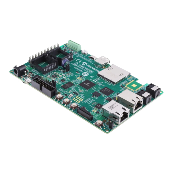
Figure 1. SAMA7G54-EK Overview
©
2022 Microchip Technology Inc.
and its subsidiaries
SAMA7G54-EK User's Guide
User Guide
SAMA7G54-EK
DS50003273A-page 1
Advertisement
Table of Contents

Related Manuals for Microchip Technology SAMA7G54-EK


Summary of Contents for Microchip Technology SAMA7G54-EK
-
Page 1: Scope
This user's guide provides detailed information on the overall design of the SAMA7G54 Evaluation Kit (SAMA7G54- EK) and describes how to use the kit. The kit is the evaluation platform for the SAMA7G5 Series devices. Figure 1. SAMA7G54-EK Overview User Guide DS50003273A-page 1 ©... -
Page 2: Introduction
Data sheet DS20005514 ATWILC3000-MR110xA Data sheet DS70005327 ATECC608B Data sheet DS40002239 PAC1934 Data sheet DS20005850 How to Manually Solder the ATWILC3000 Module on an MPU Board Application note AN3227 User Guide DS50003273A-page 2 © 2022 Microchip Technology Inc. and its subsidiaries... -
Page 3: Product Overview
Product Overview Product Overview The SAMA7G54 Evaluation Kit (SAMA7G54-EK) provides a versatile Total System Solution platform that highlights Microchip MPU and connectivity ICs. The board features on-board memories, two Ethernet interfaces, three USB ports, two CAN interfaces, one SD card ™... -
Page 4: Sama7G54-Ek Content
160 x 100 mm RoHS status Compliant Power Sources Two options are available to power up the SAMA7G54-EK board: • Through an external AC to DC +5V wall adapter connector (J1) • Through the USB Micro-AB connector on the USBA port (J7) Table 2-3. -
Page 5: On-Board Connectors
Maximum 3.3 VDC current 300 mA The SAMA7G54-EK board runs at a 3.3V voltage level logic. The maximum voltage that the I/O pins can CAUTION tolerate is 3.3V. Providing higher voltages (e.g. 5V) to an I/O pin could damage the board. -
Page 6: Default Jumper Settings
JTAG, 20-pin IDC Default Jumper Settings The following picture shows the default jumper settings. Jumpers in blue are in open position, jumpers in red are in closed position. User Guide DS50003273A-page 6 © 2022 Microchip Technology Inc. and its subsidiaries... - Page 7 SAMA7G54-EK Product Overview Figure 2-2. SAMA7G54-EK Default Jumper Settings Table 2-5. SAMA7G54-EK Jumper Settings Jumper State Function Closed VDDBU current measurement Open (default) RMII Ethernet interface is selected. Closed The 4-microphone PDMIC interface is selected. Booting from on-board memory is permanently allowed and only disabled during SW4 Open (default) pressure.
-
Page 8: Function Blocks
This document is not intended to provide detailed information about the processor or about any other components used on the board. Refer to the components documentation for further details. Figure 3-1. SAMA7G54-EK Block Diagram Raspberry Pi USB 2.0 Host Type A... -
Page 9: Power Supply Topology And Power Distribution
SAMA7G5 Series data sheet must be respected for a reliable operation of the device. 3.1.1 Input Power Options The SAMA7G54-EK board can be powered through: • An external AC to DC +5V wall adapter connected via a 2.1 mm center-positive plug into the power jack of the board (J1);... - Page 10 External Power Switch 5V_DC 5V_MAIN SIA923AEDJ-T1-GE3 SIA923AEDJ-T1-GE3 0.1uF 100uF 22uF 0.1uF 100k 0603 0402 0402 1210 1206 0402 100k 0402 USB_VBUS_5V 0603 SIA923AEDJ-T1-GE3 120R BLM18PG121SN1D 10uF 0.1uF SIA923AEDJ-T1-GE3 1206 0402 User Guide DS50003273A-page 10 © 2022 Microchip Technology Inc. and its subsidiaries...
- Page 11 1.1V DC/DC supplies SAMA7G5 core (VDDCORE). • 1.275V DC/DC supplies SAMA7G5 CPU (VDDCPU). • 1.8V LDO supplies the SD Card interface and the e.MMC. The figure below shows the power management scheme. User Guide DS50003273A-page 11 © 2022 Microchip Technology Inc. and its subsidiaries...
- Page 12 A resistor swap must be performed for this configuration. The figure below shows the shutdown connection and the reset circuitry. User Guide DS50003273A-page 12 © 2022 Microchip Technology Inc. and its subsidiaries...
- Page 13 3.1.5 Power Measurement One Microchip DC power/energy monitor is embedded on the SAMA7G54-EK board and provides a four-channel current sense monitoring ensured by the PAC1934 device. The device communicates with the MPU via a Two-Wire Interface (TWI) and an alert output signal.
- Page 14 TWI data signal PAC1935_INT_PC8 – PAC1934 interrupt Table 3-3. PAC1934 TWI Address Device 7-bit Client Address Full Address with RD/WR# PAC1934 TWI Read 0x21 0010_000 PAC1934 TWI Write 0x20 User Guide DS50003273A-page 14 © 2022 Microchip Technology Inc. and its subsidiaries...
-
Page 15: Processor
3.3V for I/Os, oscillators and digital power rails (VDDIN33, VDDUTMII, VDDIOP0, VDDIOP1, VDDQSPI1, VDDSDMMC2, etc.) Decoupling capacitors are placed close to the MPU power pins to stabilize the voltage rails. User Guide DS50003273A-page 15 © 2022 Microchip Technology Inc. and its subsidiaries... - Page 16 0.1uF VBAT GNDBAT VDDANA 0201 0.1uF VDDDPHY GNDDPHY 0201 0.1uF VDDDPHY GNDDPHY SAMA7G54 3.2.2 Configuration and Control This figure shows the main block for processor configuration and control. User Guide DS50003273A-page 16 © 2022 Microchip Technology Inc. and its subsidiaries...
- Page 17 SDMMC2 calibration AUDIOCLK Output Audio clock output ADVREFP Input Voltage reference for the embedded analog comparator HHSx_Dx Three USB ports embedded inside the MPU HHSx_RTUNE Input USB external tuning User Guide DS50003273A-page 17 © 2022 Microchip Technology Inc. and its subsidiaries...
- Page 18 DSC6003MA3B-032K768), using the PCB footprint reservation (Y4). In that case, remove crystal Y1 and capacitors C66 and C72, and populate resistor R38 and capacitor C77 with the appropriate MEMS (Y4). User Guide DS50003273A-page 18 © 2022 Microchip Technology Inc. and its subsidiaries...
- Page 19 The SAMA7G5 MPU embeds a Universal DDR Memory Controller (UDDRC) to drive the DDR2, DDR3, LPDDR2 and LPDDR3 memories. The following figure shows the UDDRC controller schematic and controller layout recommendations. User Guide DS50003273A-page 19 © 2022 Microchip Technology Inc. and its subsidiaries...
- Page 20 SAMA7G5 Series data sheet for the DDR3L case, the resistor value is 240 Ohms. The DDR_VREF pin serves as a voltage reference input for the DDR I/Os when DDR or LPDDR external SDRAM memories are used. User Guide DS50003273A-page 20 © 2022 Microchip Technology Inc. and its subsidiaries...
- Page 21 The PIOA bank is mainly used for the e.MMC memory and Gigabit Ethernet over power rails VDDSDMMC0 and VDDIOP0, respectively. The following schematic shows the PIOA bank distribution. User Guide DS50003273A-page 21 © 2022 Microchip Technology Inc. and its subsidiaries...
- Page 22 PA11 VDDSDMMC0 SDMMC0_DS e.MMC data strobe PA12 VDDIOP0 PA12 User button PA13 VDDIOP0 PWMH2 Green LED control or mikroBUS 1 PWM control PA14 VDDIOP0 SDMMC0_CD e.MMC card detect User Guide DS50003273A-page 22 © 2022 Microchip Technology Inc. and its subsidiaries...
- Page 23 The PIOB bank is mainly used for the SPI interface, QSPI and SD Card over power rails VDDIOP0, VDDQSPI1/0 and VDDSDMMC1, respectively. The following schematic shows the PIOB bank distribution. User Guide DS50003273A-page 23 © 2022 Microchip Technology Inc. and its subsidiaries...
- Page 24 PB12 VDDQSPI0 QSPI0_IO0 Octal SPI0 I/O line 0 PB13 VDDQSPI0 QSPI0_CS Octal SPI0 Chip Select PB14 VDDQSPI0 QSPI0_SCK Octal SPI0 serial clock PB15 VDDQSPI0 PB15 MCP16502 HPM control User Guide DS50003273A-page 24 © 2022 Microchip Technology Inc. and its subsidiaries...
- Page 25 SD Card data line 0 3.2.5.3 PIOC Bank The PIOC bank is mainly used for the UART and TWI interfaces, over power rail VDDIN33. The following schematic shows the PIOC bank distribution. User Guide DS50003273A-page 25 © 2022 Microchip Technology Inc. and its subsidiaries...
- Page 26 TWI clock line for ECC608, RPi CSI camera, EEPROM1 or EEPROM2 PC13 VDDIN33 FLEXCOM8_IO1 devices TWI data line for ECC608, RPi CSI camera, EEPROM1 or EEPROM2 PC14 VDDIN33 FLEXCOM8_IO0 devices User Guide DS50003273A-page 26 © 2022 Microchip Technology Inc. and its subsidiaries...
- Page 27 The PIOD bank is mainly used for the WILC3000 radio module and Ethernet 10/100, over power rails VDDSDMMC2 and VDDIOP1, respectively. The following schematic shows the PIOD bank distribution. User Guide DS50003273A-page 27 © 2022 Microchip Technology Inc. and its subsidiaries...
- Page 28 PD12 VDDIOP1 CANTX0 CAN transmit line 0 PD13 VDDIOP1 CANRX0 CAN receive line 0 PD14 VDDIOP1 CANTX1 CAN transmit line 1 PD15 VDDIOP1 CANRX1 CAN receive line 1 User Guide DS50003273A-page 28 © 2022 Microchip Technology Inc. and its subsidiaries...
- Page 29 VDDIOP1 ATWILC3000 enable control signal VDDIOP1 RPi connector SPI chip enable 2 or RPi CSI camera GPIO VDDIOP1 PWML0/PE2 RPi connector PWM signal or RPi CSI camera GPIO User Guide DS50003273A-page 29 © 2022 Microchip Technology Inc. and its subsidiaries...
- Page 30 Interfaces Distribution 3.2.5.6.1 TWI Bus Distribution The SAMA7G54-EK features three dedicated TWIs to access the on-board devices. The TWI interface uses only two lines, namely serial data (TWD) and serial clock (TWCK). According to the standard, the TWI clock rate is limited to 400 kHz in Fast mode and 100 kHz in Normal mode, but a configurable baud rate generator enables adapting the output data rate to a wide range of core clock frequencies.
- Page 31 EXT40_TWCK_PC19 3.2.5.6.2 SPI Bus Distribution The SAMA7G54-EK features two dedicated SPIs to access the on-board devices. The Serial Peripheral Interface (SPI) circuit is a synchronous serial data link that provides communication with external devices in Host or Client mode. It also enables communication between processors if an external processor is connected to the system.
- Page 32 Figure 3-24. Second SPI Distribution Schematic 0402 1% EXT40_SPI1_MOSI_PE3 0402 1% BT_RX_FLEXCOM0_IO0_PE3 0402 1% EXT40_SPI1_MISO_PE4 0402 1% BT_TX_FLEXCOM0_IO1_PE4 0402 1% EXT40_SPI1_CE0_PE6 0402 1% BT_RTS_FLEXCOM0_IO3_PE6 0402 1% EXT40_SPI1_CE1_PE7 0402 1% BT_CTS_FLEXCOM0_IO4_PE7 EXT40_SPI1_SCLK_PE5 EXT40_SPI1_SCLK_PE5 User Guide DS50003273A-page 32 © 2022 Microchip Technology Inc. and its subsidiaries...
- Page 33 EXT40_SPI1_SCLK_PE5 SPI clock line RPi 40-pin connector 3.2.5.6.3 GPIO Distribution The SAMA7G54-EK features one QuickSwitch 2:1 multiplexer to distribute the MPU PIOs. The multiplexer distributes the PIOs according to the J3 status: • J3 is open (default mode): the Ethernet 10/100 interface is distributed.
- Page 34 Receive data valid or carrier sense and data valid PD24 PD24 PDMC0_DS1_PD24 PDM data line 1 3.2.5.6.4 Shared GPIO Resources The SAMA7G54-EK embeds several GPIOs shared between two devices/interfaces. The schematic below describes the sharing information. Figure 3-26. GPIO Sharing Schematic 0402 1% PA13 LED_GREEN_PA13...
-
Page 35: On-Board Memories
The SAMA7G5 MPU features a Universal DDR Memory Controller (UDDRC), a Quad Serial Peripheral Interface (QSPI) and a Secure Digital MultiMedia Card Controller (SDMMC) to enable interfacing to a wide range of external memories. This section describes the memory devices mounted on the SAMA7G54-EK board: • One 16-bit, 4-Gbit DDR3L SDRAM •... - Page 36 0201 0201 AS4C256M16D3LC-12BCNTR 3.3.2 e.MMC Memory The SAMA7G54-EK supports e.MMC NAND Flash memory through its Secure Digital Multimedia Controller (SDMMC), and the board implements an S40FC004C1B1C00000, 32-Gb e.MMC NAND Flash to provide a 4-Gbyte memory space. User Guide DS50003273A-page 36 ©...
- Page 37 7 PA11 SDMMC0_DS_PA11 – e.MMC data strobe To enable booting on e.MMC, the PA14 I/O must be grounded. A circuitry is available on the SAMA7G54-EK board to enable/disable boot from e.MMC. See Disable Boot for more details. 3.3.3 Octal Serial Flash The SAMA7G54-EK board features one Quad Serial Peripheral Interface (QSPI) memory MX66LM1G45GXDI00.
- Page 38 NRST_OUT 3.3.4 Dual Serial EEPROM The SAMA7G54-EK board embeds two Microchip 24AA025E48 serial Electrically-Erasable Programmable Read- Only Memories (EEPROMs). The 24AA025E48 features 2048 bits of serial EEPROMs organized as 256 words of eight bits each and is accessed via an I C-compatible (2-wire) serial interface.
-
Page 39: Peripheral Interfaces
0xA6 Peripheral Interfaces Several interfaces and connectors are implemented in the SAMA7G54-EK to enable the user to test all the features offered by the MPU and to facilitate a reference design for future customer applications. This section describes the following peripherals mounted on the SAMA7G54-EK board:... - Page 40 100R 0402 nRST_OUT KSZ8081RNAIA-TR R181 C192 ETH1_XI_25M 20pF 0402 120R R182 R183 0402 25MHz BLM18PG121SN1D 0R 0603 10ppm 0402 ECS-250-20-33-CKM-TR R184 C193 ETH1_XO_25M GND-ETH1 GND_ETH1 20pF 0402 0402 User Guide DS50003273A-page 40 © 2022 Microchip Technology Inc. and its subsidiaries...
- Page 41 LDO controller to drive a low-cost MOSFET to supply the 1.2V core. The KSZ9131RNX offers diagnostic features to facilitate system bring-up and debugging in production testing and in product deployment. User Guide DS50003273A-page 41 © 2022 Microchip Technology Inc. and its subsidiaries...
- Page 42 Transmit data line 3 PA28 ETH0_RX2_PA28 – Receive data line 2 PA29 ETH0_RX3_PA29 – Receive data line 3 PA30 ETH0_RXCK_PA30 – Receive clock PA31 ETH0_INT_PA31 – Ethernet 0 interrupt User Guide DS50003273A-page 42 © 2022 Microchip Technology Inc. and its subsidiaries...
- Page 43 USB"). A USB host bus connector uses four pins: a power supply pin (5V), a differential pair (D+ and D- pins) and a ground pin. The SAMA7G54-EK board features three USB communication ports named USBA, USBB and USBC. 3.4.2.1 USBA Host/Device The USBA port can act as a USB device or USB host interface and can be accessed via the USB micro-B connector (J7).
- Page 44 BLM18PG121SN1D MIC2025-1YM 120R USBA_EN_5V_PB2 C195 C196 10uF 0.1uF R189 C197 C198 C199 C200 1206 0402 10uF 0.1uF 22uF 100uF 0402 1206 0402 1206 1210 USB Power Switch USBA_OVCUR_PC7 User Guide DS50003273A-page 44 © 2022 Microchip Technology Inc. and its subsidiaries...
- Page 45 The USBB_EN_5V_PC11 signal controls the current limiting power switch MIC2025, which in turn supplies power to a client device. As per the USB specification, bus-powered USB 2.0 devices are User Guide DS50003273A-page 45 © 2022 Microchip Technology Inc. and its subsidiaries...
- Page 46 The USBC_EN_5V_PC6 signal controls the current limiting power switch MIC2025, which in turn supplies power to a client device. As per the USB specification, bus-powered USB 2.0 devices are User Guide DS50003273A-page 46 © 2022 Microchip Technology Inc. and its subsidiaries...
- Page 47 – Indicates overcurrent (open drain) 3.4.3 Dual mikroBUS Click Interfaces The SAMA7G54-EK hosts two pairs of 8-pin female headers (J10 and J12) implementing the official mikroBUS socket. For details, refer to the mikroBUS documentation on www.mikroe.com/mikrobus. 3.4.3.1 mikroBUS 1 Connector The first mikroBUS 8-pin female header (J10) implements all mikroBUS features as described in the schematic below.
- Page 48 40-pin RPi connector. The end user must take care of the I²C addresses used on this nodes. The PWM feature of the first mikroBUS interface (PD20) is shared with the blue LED control. User Guide DS50003273A-page 48 © 2022 Microchip Technology Inc. and its subsidiaries...
- Page 49 3.4.4 Dual CAN Interfaces The SAMA7G54-EK features two MCP2542FD transceivers. The MCP2542FD is a high-speed CAN transceiver that provides the interface between the Controller Area Network (CAN) protocol controller and the physical two-wire bus. For more information about the MCP2542FD, refer to the product page.
- Page 50 CAN1_H Differential positive port 1 CAN1_L Differential negative port 1 3.4.5 RPi Connector Interface The SAMA7G54-EK board features a 40-pin connector (Raspberry Pi compatible) for free use. Figure 3-42. RPi 40-Pin Connector Schematic Raspberry Pi 40-pin Connector VDD_3V3 5V_MAIN FLEXCOM9_IO0...
- Page 51 This interface is shared with the mikroBUS1 and mikroBUS2 interfaces. The end user must pay attention to the I²C addresses used on these nodes. 3.4.6 RPi CSI Camera Interface The SAMA7G54-EK board features a MIPI CSI camera connector (Raspberry Pi compatible). User Guide DS50003273A-page 51 ©...
- Page 52 CAM_IO1 CAM_GPIO1_PE2 MIPI CSI LED indicator connector CAM_SCL CAM_TWCK ECC608B PC13 TWI clock line CAM_SDA CAM_TWD ECC608B PC14 TWI data line CAM_3V3 VDD_3V3 – – 3.3V power supply User Guide DS50003273A-page 52 © 2022 Microchip Technology Inc. and its subsidiaries...
- Page 53 3.4.8 Quad MEMS Microphones The SAMA7G54-EK embeds four digital MEMS microphones SPK0641HT4H-1. Those microphones convert acoustic pressure waves into a digital signal. This signal is acquired by the SAMA7G5 MPU through a PDMIC interface as shown in the following schematic.
- Page 54 The module is available in a fully certified, 22.428 x 17.732 mm, 36-pin module package. For more information about the ATWILC3000, refer to the product page. User Guide DS50003273A-page 54 © 2022 Microchip Technology Inc. and its subsidiaries...
- Page 55 The MCP1725 was chosen because it can supply the current required by the module, and because it features a shutdown input pin (SHDN) and a power good output pin (PWRGD): • The SHDN input allows to shut down the wireless module when unused, therefore saving power. User Guide DS50003273A-page 55 © 2022 Microchip Technology Inc. and its subsidiaries...
- Page 56 The SD (Secure Digital) Card is a non-volatile memory card format used as a mass storage memory in mobile devices. The SAMA7G54-EK has one Secure Digital Multimedia Card (SDMMC) interface that supports the MultiMedia Card (e.MMC) specification V4.51, the SD Memory Card specification V3.0, and the SDIO V3.0 specification. It is compliant with the SD Host Controller Standard V3.0 specification.
- Page 57 (R262 must be populated) "NRST_OUT" signal. This action disables the MIC94085YFT power switch and VDD_SDCARD is forced to ground. For more details about the MIC94085YFT power switch, refer to the product page. User Guide DS50003273A-page 57 © 2022 Microchip Technology Inc. and its subsidiaries...
- Page 58 Table 3-41. ECC608B PIO Signal Descriptions Signal MPU Signal Name Device Signal Name Shared With Description PC14 FLEXCOM8_IO0_PC14 ECC608_TWD MIPI CSI camera TWI data PC13 FLEXCOM8_IO1_PC13 ECC608_TWCK MIPI CSI camera TWI clock User Guide DS50003273A-page 58 © 2022 Microchip Technology Inc. and its subsidiaries...
- Page 59 ECC608B TWI Write 0xC0 3.4.12 Tamper Pins Connector The SAMA7G54-EK board features four tamper pins for static or dynamic intrusion detections. For a description of intrusion detection, refer to the SAMA7G5 Series data sheet, section “Security Module (SECUMOD)”. See Reference Documents.
-
Page 60: User Interaction And Debugging
R234 and R235. If a 3-wire FTDI cable is used, a shortcut between VBUS_FTDI and VDD_3V3 is necessary. 3.5.2 Debug JTAG A 20-pin JTAG header (J27) is provided on the SAMA7G54-EK board to facilitate software development and debugging using various JTAG emulators. The interface signals have a voltage level of 3.3V. User Guide DS50003273A-page 60 ©... - Page 61 3.5.3 Embedded Debugger (J-Link-OB) Interface The SAMA7G54-EK includes a built-in SEGGER J-Link-On-Board (J-Link-OB) device. The functionality is implemented with an ATSAM3U4C microcontroller in an LFBGA100 package. The ATSAM3U4C provides the functions of the JTAG interface and a bridge from USB to the serial debug port (CDC, or Communication Device Class).
- Page 62 It is capable of sourcing up to 500 mA of output current while only drawing 38 μA of operating current. For more information about the MIC5528, refer to the product page. User Guide DS50003273A-page 62 © 2022 Microchip Technology Inc. and its subsidiaries...
- Page 63 The USB CDC converts the USB device into a serial communication device. The target device running the CDC is recognized by the host as a serial interface (USB2COM, virtual COM port) without the need to install a special host User Guide DS50003273A-page 63 © 2022 Microchip Technology Inc. and its subsidiaries...
- Page 64 USB, such as a terminal program. 3.5.5 Push Button Switches The SAMA7G54-EK features three push buttons: • One user push button (SW1) connected to PIO_PA12 for free use.
- Page 65 3.5.7 RGB LED The SAMA7G54-EK board features one RGB (red, green, blue) LED. The three LED cathodes are controlled via one standard GPIO and two GPIOs in PWM mode. At Reset state, the blue and green LEDs are off; only the red LED is on, representing the "power on" status.
- Page 66 Function Blocks Table 3-47. RGB LED PIOs Signal Shared With Function LED_BLUE_PD20 PD20 mikroBUS 2 connector PWMH3 LED_GREEN_PA13 PA13 mikroBUS 1 connector PWMH2 LED_RED_PB8 RPi 40-pin connector GPIO User Guide DS50003273A-page 66 © 2022 Microchip Technology Inc. and its subsidiaries...
-
Page 67: Installation And Operation
• An AC/DC wall adapter (not provided in the kit box) in case of high power consumption system Board Setup Follow these steps before using the SAMA7G54-EK: Unpack the board, taking care to avoid electrostatic discharge. Check the Default Jumper Settings. - Page 68 It is possible to setup an automatic startup at each power insertion by mounting a C240 capacitor. With this configuration, the system starts automatically when the USB cable (J7) or the DC jack (J1) is connected. This is not the factory configuration. User Guide DS50003273A-page 68 © 2022 Microchip Technology Inc. and its subsidiaries...
-
Page 69: Ordering Information
SAMA7G54-EK Ordering Information Ordering Information Table 5-1. Evaluation Kit Ordering Information Ordering Code Board Marking EV21H18A SAMA7G54-EK EVALUATION KIT User Guide DS50003273A-page 69 © 2022 Microchip Technology Inc. and its subsidiaries... -
Page 70: Appendix A. Schematics And Layouts
SAMA7G54-EK Appendix A. Schematics and Layouts Appendix A. Schematics and Layouts Figure 6-1. SAMA7G54-EK: Schematic Page 1 SAMA7G5-EK Drawn By: Engineer: FIDUCIAL ROUND PCB 1mm SMD PartNumber: Project Title EV21H18A SAMA7G54 Evaluation Kit Sheet Title Variant Name Designed with Block Diagram... - Page 71 SAMA7G54-EK Appendix A. Schematics and Layouts Figure 6-2. SAMA7G54-EK: Schematic Page 2 PMIC External 5V Input Power and Input Power protection (5V0) 5V_MAIN 0603 PVIN1 0603 4.7uF 5V_EXT 5V_DC HPM_PB15 0402 0402 SHDN PWRHLD PGND1 PMEG3030EP 22uF 10uF 10uF VDD_3V3 (3V3) 5.1V...
- Page 72 SAMA7G54-EK Appendix A. Schematics and Layouts Figure 6-4. SAMA7G54-EK: Schematic Page 4 MPU decoupling MPU configuration VDDCPU VDD_3V3 0402 4.7uF 0201 0.1uF VDDCPU 0201 0.1uF HHSA_CC1 VDDCPU XOUT 0201 0.1uF XOUT HHSA_CC2 VDDCPU DIFF90 0201 0.1uF HHSA_DM USBA_N 90Ω ±15% differential trace impedance...
- Page 73 SAMA7G54-EK Appendix A. Schematics and Layouts Figure 6-6. SAMA7G54-EK: Schematic Page 6 SAMA7G5 DDR3-1066 controller 4Gb DDR3L-1600 16bit DDR_A0 DDR_D0 TP17 DDR_A1 DDR_D1 DDR_A2 DDR_D2 DDR_A3 DDR_D3 ADDR-CTL Matched Net Lengths [Tolerance = 10mil] DDR_A4 DDR_D4 SAMA7G54 DDR_A5 DDR_D5 LANE0...
- Page 74 SAMA7G54-EK Appendix A. Schematics and Layouts Figure 6-8. SAMA7G54-EK: Schematic Page 8 RGMII ETHERNET 1Gbps TRANSCEIVER BLM18PG121SN1D 120R VDD_3V3 ETH0_LED1 50Ω ± 10% single-ended trace impedance R142 R143 R144 R145 R148 R149 R150 R151 R152 R153 GND_ETH0 R146 R147 220R Matched Net Lengths [Tolerance = 0.25mm]...
- Page 75 SAMA7G54-EK Appendix A. Schematics and Layouts Figure 6-10. SAMA7G54-EK: Schematic Page 10 USB Micro-AB type connector to the USBA port (HOST/DEVICE) 5V_MAIN VDD_3V3 USBA_VBUS_5V USB_VBUS_5V USBA_VBUS_5V R185 R186 R187 USBA_VBUSDETECT_PD11 C194 R188 0402 BLM18PG121SN1D 0603 0402 20pF MIC2025-1YM 120R 0402...
- Page 76 SAMA7G54-EK Appendix A. Schematics and Layouts Figure 6-12. SAMA7G54-EK: Schematic Page 12 WILC3000 Wireless Interface 5V_MAIN VDD_3V3_WILC VOUT C215 2.2uF SENSE C216 SHDN CDELAY 0603 C217 2.2uF 1000pF PWRGD 0603 WILC3000_EN_PE0 MCP1725/3.3V VDD_3V3 VDD_3V3 VDD_3V3 0402 WILC3000_ENABLE CTS/SCL R201 R202...
- Page 77 SAMA7G54-EK Appendix A. Schematics and Layouts Figure 6-14. SAMA7G54-EK: Schematic Page 14 VDD_3V3 RGB LED User, Reset, Start Buttons R218 0402 BSS138N R219 100R 0402 R220 USER_BUTTON_PA12 TL3301NF260QG LED_BLUE_PD20 100R C238 R221 0402 VDD_3V3 0.1uF 0402 R222 0402 0402 R223...
- Page 78 SAMA7G54-EK Appendix A. Schematics and Layouts Figure 6-16. SAMA7G54-EK: Layer 1 Figure 6-17. SAMA7G54-EK: Layer 2 User Guide DS50003273A-page 78 © 2022 Microchip Technology Inc. and its subsidiaries...
- Page 79 SAMA7G54-EK Appendix A. Schematics and Layouts Figure 6-18. SAMA7G54-EK: Layer 3 Figure 6-19. SAMA7G54-EK: Layer 4 User Guide DS50003273A-page 79 © 2022 Microchip Technology Inc. and its subsidiaries...
-
Page 80: Appendix B. Unmounted Elements
24 MHz Blue Crystal selection Crystal 24 MHz Blue 24 MHz crystal Only use in factory. If mounted, the crystal Resistor 24 MHz Crystal measurement behavior will be degraded. User Guide DS50003273A-page 80 © 2022 Microchip Technology Inc. and its subsidiaries... - Page 81 LDO lines can result C220 Capacitor Supply VDD_3V3_WILC decoupling in output instability and power-on sequence failure. nSTART decoupling and startup The product starts C240 Capacitor System Blue configuration automatically. User Guide DS50003273A-page 81 © 2022 Microchip Technology Inc. and its subsidiaries...
- Page 82 R249 Resistor J-Link-OB Boundary scan selection boundary scan. J-Link- OB will never start. nRST selection instead of R134 Resistor nRST_OUT Blue Remove R136. NRST_OUT User Guide DS50003273A-page 82 © 2022 Microchip Technology Inc. and its subsidiaries...
-
Page 83: Soldering The Wi-Fi/Bt Module
Extra care must be taken when assembling the ATWILC3000-MR110xA Wi-Fi/BT module. Refer to the application note "How to Manually Solder the ATWILC3000 Module on an MPU Board". See Reference Documents. User Guide DS50003273A-page 83 © 2022 Microchip Technology Inc. and its subsidiaries... -
Page 84: Revision History
SAMA7G54-EK Revision History Revision History DS50003273A - 03/2022 First issue. User Guide DS50003273A-page 84 © 2022 Microchip Technology Inc. and its subsidiaries... -
Page 85: Table Of Contents
SAMA7G54-EK Table of Contents Scope................................1 Introduction............................. 2 1.1. Document Layout......................... 2 1.2. Reference Documents........................2 Product Overview............................3 2.1. SAMA7G54-EK Features......................3 2.2. SAMA7G54-EK Content.......................4 2.3. Evaluation Kit Specifications......................4 2.4. Power Sources..........................4 2.5. On-Board Connectors........................5 2.6. Default Jumper Settings....................... 6 Function Blocks............................8... - Page 86 SAMA7G54-EK Worldwide Sales and Service........................90 User Guide DS50003273A-page 86 © 2022 Microchip Technology Inc. and its subsidiaries...
-
Page 87: The Microchip Website
It is your responsibility to ensure that your application meets with your specifications. Contact your local Microchip sales office for additional support or, obtain additional support at www.microchip.com/en-us/support/ design-help/client-support-services. User Guide DS50003273A-page 87 © 2022 Microchip Technology Inc. and its subsidiaries... -
Page 88: Trademarks
The Adaptec logo, Frequency on Demand, Silicon Storage Technology, Symmcom, and Trusted Time are registered trademarks of Microchip Technology Inc. in other countries. GestIC is a registered trademark of Microchip Technology Germany II GmbH & Co. KG, a subsidiary of Microchip Technology Inc., in other countries. -
Page 89: Quality Management System
TrustZone, ULINK, ULINK2, ULINK-ME, ULINK-PLUS, ULINKpro, µVision, Versatile are trademarks or registered trademarks of Arm Limited (or its subsidiaries) in the US and/or elsewhere. Quality Management System For information regarding Microchip’s Quality Management Systems, please visit www.microchip.com/quality. User Guide DS50003273A-page 89 © 2022 Microchip Technology Inc. and its subsidiaries... - Page 90 Tel: 631-435-6000 Sweden - Stockholm San Jose, CA Tel: 46-8-5090-4654 Tel: 408-735-9110 UK - Wokingham Tel: 408-436-4270 Tel: 44-118-921-5800 Canada - Toronto Fax: 44-118-921-5820 Tel: 905-695-1980 Fax: 905-695-2078 User Guide DS50003273A-page 90 © 2022 Microchip Technology Inc. and its subsidiaries...
Need help?
Do you have a question about the SAMA7G54-EK and is the answer not in the manual?
Questions and answers