Table of Contents
Advertisement
Quick Links
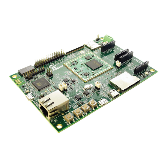
SAMA5D27 SOM1 Kit1 User's Guide
Scope
This user's guide provides detailed information on the overall design of the SAMA5D27 SOM1 Kit1 and
describes how to use the kit.
The kit is the evaluation platform for the SAMA5D27 SIP (System-In-Package) and SOM (System-On-
Module), and comprises:
•
a baseboard
•
a SAMA5D27 SOM soldered on the baseboard
•
a SAMA5D27 SIP soldered on the SOM
•
a USB cable
See the figure below.
Figure 1. SAMA5D27 SOM1 Kit1 Overview
Baseboard
©
2018 Microchip Technology Inc.
SAMA5D27 SOM1 Kit1
SOM (System-On-Module)
User Guide
SIP (System-In-Package)
DS50002667C-page 1
Advertisement
Table of Contents

Related Manuals for Microchip Technology SAMA5D27 SOM1 Kit1


Summary of Contents for Microchip Technology SAMA5D27 SOM1 Kit1
-
Page 1: Scope
SAMA5D27 SOM1 Kit1 User's Guide Scope This user's guide provides detailed information on the overall design of the SAMA5D27 SOM1 Kit1 and describes how to use the kit. The kit is the evaluation platform for the SAMA5D27 SIP (System-In-Package) and SOM (System-On- Module), and comprises: •... -
Page 2: Table Of Contents
SAMA5D27 SOM1 Kit1 Table of Contents Scope..........................1 1. Introduction........................3 1.1. Document Layout......................... 3 1.2. Reference Documents........................3 2. Product Overview...................... 4 2.1. Kit Contents..........................4 2.2. Features............................4 2.3. Specifications..........................5 2.4. Power Sources..........................5 3. Baseboard Components....................7 3.1. Baseboard Overview........................7 3.2. -
Page 3: Introduction
SAMA5D27 SOM1 Kit1 Introduction Introduction Document Layout The document is organized as follows: • Introduction • Product Overview – Important information about the kit • Board Components – Specifications of the kit and high-level description of the major components and interfaces •... -
Page 4: Product Overview
SAMA5D27 SOM1 Kit1 Product Overview Product Overview Kit Contents The kit includes the following: • One baseboard with soldered SOM • One USB cable Features The kit comprises a baseboard with a soldered SAMA5D27 SOM1 module. The module features a SAMA5D27-D1G-CU SIP embedding a 1-Gbit DDR2 SDRAM. -
Page 5: Specifications
SAMA5D27 SOM1 Kit1 Product Overview ...continued Characteristics Specifications Components Debug port One J-Link-OB and J-Link-CDC Microchip SAM3U micro-controller with embedded J-Link firmware One JTAG interface – Board Monitor One RGB (Red, Green, Blue) LED – Four push button switches Power ON, Reset, Wakeup, User Free... - Page 6 SAMA5D27 SOM1 Kit1 Product Overview Table 2-3. Electrical Characteristics Electrical Parameter Value Input voltage 5VCC Maximum input voltage 6VCC Maximum 3.3VDC current available 1.2A I/O voltage 3.3V only User Guide DS50002667C-page 6 © 2018 Microchip Technology Inc.
-
Page 7: Baseboard Components
Baseboard Components Baseboard Components This section covers the specifications of the SAMA5D27 SOM1 Kit1 baseboard and provides a high-level description of the baseboard's major components and interfaces. This document is not intended to provide a detailed documentation about the processor or about any other component used on the baseboard. - Page 8 SAMA5D27 SOM1 Kit1 Baseboard Components Figure 3-2. SAMA5D27 SOM1 Kit1 Block Diagram USB A&B ECC608 SD Card Flash Connector GPIO POWER Connector System Supplies USB-B 3v3, 1v8 REGULATOR Connector QSPI CRYPTO SDHC1 3.3V, 1.8V Power Power Power Switch VDDBU Switch SDHC0...
- Page 9 Closed Enables 3.3V power mikroBUS1 (closed=enable) Closed Enables 3.3V power mikroBUS2 (closed=enable) 3.1.2 Baseboard Connectors The following table describes the interface connectors on the SAMA5D27 SOM1 Kit1 baseboard. Table 3-2. Baseboard Interface Connectors Connector Interfaces to CLK_AUDIO test point (not populated)
-
Page 10: Function Blocks
SAMA5D27 SOM1 Kit1 Baseboard Components ...continued Connector Interfaces to J29-J30 mikroBUS2 connectors Tamper and analog comparator connector SHDN test point (not populated) Function Blocks 3.2.1 SAMA5D27 SOM1 The SAMA5D27 SOM1 main features are as follows: ® ® • Ultra-small SIP (SAMA5D27-D1G-CU) embedding an ultra-low-power SAMA5D27 Arm... - Page 11 SAMA5D27 SOM1 Kit1 Baseboard Components 3.2.2 Power Supply Topology and Power Distribution 3.2.2.1 Input Power Options The board power source can come through either a USB connector (J10 or J17) connected to a PC or a 5V DC-USB power supply unit. These USB power sources are sufficient to supply the board in most applications.
- Page 12 SAMA5D27 SOM1 Kit1 Baseboard Components While the external power is being applied, the baseboard can be shut down by software and then woken up by action on the PB2 push button, which activates the WKUP signal. The figure below shows the power management scheme.
- Page 13 SAMA5D27 SOM1 Kit1 Baseboard Components Figure 3-7. SOM Power Lines VDDIN_3V3 VDDIN_3V3_1 GND_0 VDDIN_3V3_2 GND_1 GND_2 2.2uF 0.1uF 0.1uF GND_3 GND_4 VDDBU 0603 0402 0402 GND_5 GND_6 VDDBU GND_7 GND_8 GND_9 2.2uF 0.1uF GND_10 VDDIN_3V3 GND_11 0603 0402 GND_12 VDDISC GND_13...
- Page 14 SAMA5D27 SOM1 Kit1 Baseboard Components • One reset push button (PB1). When pressed and released, the baseboard is reset. • One wake-up push button (PB2) connected to the SAMA5D27 WKUP pin, used to exit the processor from Backup mode. •...
- Page 15 SAMA5D27 SOM1 Kit1 Baseboard Components 3.2.5.1 CS Disable Boot One jumper (J13) controls the selection (CS#) of the bootable memory components (QSPI) using a non- inverting 3-state buffer. Figure 3-13. CS Disable Boot VDD_3V3 0402 VDD_3V3 (SOM) HDR-2.54 Male 1x2 DISABLE_BOOT...
- Page 16 SAMA5D27 SOM1 Kit1 Baseboard Components Figure 3-14. SDMMC0 VDDSDHC VDD_3V3 0402 10uF 0.1uF 0603 1206 1206 0402 0402 0402 0402 SDMMC0_WP PA12 SDMMC0_DA1 SDMMC0_DA0 SDMMC0_CD PA13 SDMMC0_CK SDMMC0_CDA SDMMC0_DA3 SDMMC0_DA2 SD_MMCPlus_CARD SDMMC0_DA4 SDMMC0_DA5 SDMMC0_DA6 SDMMC0_DA7 Figure 3-15. Standard SD Socket J12 Location The table below describes the pin assignment of SDMMC connector J12.
- Page 17 SAMA5D27 SOM1 Kit1 Baseboard Components ...continued Pin No Mnemonic Signal Description – VDDSDHC (3.3V or – Power line 1.8V) SDMMC0_CK_PA0 Clock line SDMMC0_CD_PA13 PA13 Card detect SDMMC0_DAT0_PA2 Data line SDMMC0_DAT1_PA3 Data line SDMMC0_DAT2_PA4 Data line SDMMC0_DAT4_PA6 Data line SDMMC0_DAT5_PA7 Data line...
- Page 18 SAMA5D27 SOM1 Kit1 Baseboard Components Figure 3-17. microSD Socket J14 Location The table below describes the pin assignment of microSD connector J14. Table 3-7. microSD Socket J14 Pin Assignment Pin No Mnemonic Signal Description SDMMC1_DAT2 PA20 Data bit 2 SDMMC1_DAT3 PA21 Data bit 3...
- Page 19 SAMA5D27 SOM1 Kit1 Baseboard Components ...continued Pin No Mnemonic Signal Description – Common ground – Common ground – Common ground ™ 3.2.6.4 CryptoAuthentication ATECC608A is a member of the CryptoAuthentication family of crypto engine authentication devices with highly secure hardware-based key storage.
- Page 20 SAMA5D27 SOM1 Kit1 Baseboard Components Figure 3-19. Ethernet PHY TX_P TX_N RX_P RX_N 0.1uF 0.1uF 0402 0402 GND_ETH Right yellow LED Left Green LED EARTH_ETH EARTH_ETH VDD_3V3 RJ45 J00-0061 RJ45 LINK ETH_LED0 ETH_LED0 470R Figure 3-20. Ethernet RJ45 Connector J15 Location The table below describes the pin assignment of Ethernet connector J15.
- Page 21 SAMA5D27 SOM1 Kit1 Baseboard Components ...continued Pin No Mnemonic Signal Description Decoupling capacitor – Decoupling capacitor – Receive negative differential pair – EARTH / GND Common ground ACT LED (A) LED activity (not used) ACT LED (K) LED activity (not used)
- Page 22 SAMA5D27 SOM1 Kit1 Baseboard Components The USB-A port (J17) features a VBUS insert detection function through ladder-type resistors R70 and R71. Figure 3-21. USB-A Type microAB Connector VBUS_USBA USBA_VBUS_5V PD20 100k 0402 0.1uF 200k 20pF 0402 0402 0402 VBUS USBA_N USBA_DM...
- Page 23 SAMA5D27 SOM1 Kit1 Baseboard Components Table 3-11. USB-A Connector J17 Pin Assignment Pin No Mnemonic Signal Description VBUS 5V power Data minus Data plus On-the-go identification Common ground 3.2.7.4 USB-B Interface The figure below shows the USB implementation on the USB-B port terminated on USB Type C connector J19.
- Page 24 SAMA5D27 SOM1 Kit1 Baseboard Components Figure 3-24. USB-B Type C Connector J19 Location The table below describes the pin assignment of USB-B connector J19. Table 3-12. USB-B Connector J19 Pin Assignment Pin No Mnemonic Signal Description Ground return SSTXp1 SuperSpeed differential pair #1, TX, positive (NOT USED)
- Page 25 SAMA5D27 SOM1 Kit1 Baseboard Components ...continued Pin No Mnemonic Signal Description Ground return Ground return SSRXp1 SuperSpeed differential pair #1, RX, positive (NOT USED) SSRXn1 SuperSpeed differential pair #1, RX, negative (NOT USED) VBUS Bus power SBU2 Sideband use (SBU) USB 2.0 differential pair, position 2, negative...
- Page 26 SAMA5D27 SOM1 Kit1 Baseboard Components 3.2.7.5 HSIC Interface High-Speed Inter-Chip (HSIC) is a standard for USB chip-to-chip interconnect with a 2-signal (strobe, data) source synchronous serial interface using 240 MHz DDR signaling to provide only high-speed 480 Mbps data rate.
-
Page 27: External Interfaces
SAMA5D27 SOM1 Kit1 Baseboard Components Figure 3-28. CAN Connector J16 Location Table 3-14. CAN Connector J16 Pin Assignment Mnemonic Signal Description CANH Differential positive CANL Differential negative Ground External Interfaces 3.3.1 LCD TFT Interface The baseboard provides a FPC connector with 24 bits of data and control signals to the LCD interface. - Page 28 SAMA5D27 SOM1 Kit1 Baseboard Components Figure 3-29. LCD Expansion Header Interface VDD_MAIN_5V VDD_3V3 0R0402 0R0402 0R0402 NRST LCDPWM LCD_PWM_PC3 IRQ2 PC25 IRQ1 TWCK_LCD TWD_LCD LCDDISP SPI0_NPCS0 PA17 SPI0_ MISO PA16 SPI0_ MOSI PA15 SPI0_ SPCK PA14 LCDDEN LCDHSYNC LCDVSYNC LCDPCK LCDDAT23...
- Page 29 SAMA5D27 SOM1 Kit1 Baseboard Components Figure 3-30. LCD Connector J26 Location The table below describes the pin assignment of LCD connector J26. Table 3-15. LCD Connector J26 Pin Assignment Pin No Signal Signal RGB Interface Function PA17 Shared with SPI_NPCS0 pin 40...
- Page 30 SAMA5D27 SOM1 Kit1 Baseboard Components ...continued Pin No Signal Signal RGB Interface Function – LCDDAT8 PB19 Data line (GREEN0) LCDDAT9 PB20 Data line (GREEN1) LCDDAT10 PB21 Data line (GREEN2) LCDDAT11 PB22 Data line (GREEN3) – – LCDDAT12 PB23 Data line (GREEN4)
- Page 31 SAMA5D27 SOM1 Kit1 Baseboard Components ...continued Pin No Signal Signal RGB Interface Function TWCK TWI_SCL I2C clock line (maXTouch) GPIO IRQ1 maXTouch interrupt line GPIO PC25 IRQ2 Interrupt line for other I2C devices LCDPWM Backlight control RESET nRST RESET Reset for both display and maXTouch Main_5V/3V3 3.3V or 5V supply (R81/R83 selected)
- Page 32 SAMA5D27 SOM1 Kit1 Baseboard Components Figure 3-32. ISC Connector J27 Location The table below describes the pin assignment of ISC connector J27. Table 3-16. ISC Connector J27 Pin Assignment SAMA5D27 Signal Pin No Signal SAMA5D27 Function Function 3.3V power – VDD_3V3 –...
-
Page 33: Debugging Capabilities
SAMA5D27 SOM1 Kit1 Baseboard Components ...continued SAMA5D27 Signal Pin No Signal SAMA5D27 Function Function Ground – ISC_PCK PC21 Clock Ground – ISC_D0 Data0 Data1 PC10 ISC_D1 ISC_D2 PC11 Data2 Data3 PC12 ISC_D3 ISC_D4 PC13 Data4 Data5 PC14 ISC_D5 ISC_D6 PC15... - Page 34 SAMA5D27 SOM1 Kit1 Baseboard Components • One UART through USB J-Link-CDC • Two JTAG interfaces, one connected from the MPU using connector J11 and one through the J- Link-OB interface USB port J10 3.4.1 Debug JTAG This section describes the signals and connectors related to the JTAG interface.
- Page 35 SAMA5D27 SOM1 Kit1 Baseboard Components ...continued Pin No Mnemonic Signal Description TMS TEST MODE SELECT JTAG mode set input into target processor Common ground TCK TEST CLOCK - Output timing signal, for synchronizing test logic and control JTAG clock signal into target processor...
- Page 36 SAMA5D27 SOM1 Kit1 Baseboard Components Figure 3-36. J-Link-OB Interface VDD_3V3_3U ENSPI VDD_3V3_3U Side Side NRST_3U TDI_3U TDO_3U TRSTIN TDO/TRACESWO PA0/PGMNCMD 0R0402 TCK_3U TRSTOUT TCK/SWCLK PA1/PGMRDY TMS_3U TMS/SWDIO PA2/PGMNOE TRESIN NRST PA3/PGMNVALID NRST 150R TRESOUT 100R ERASE PA4/PGMM0 VDD_3V3_3U pads on PCB...
- Page 37 SAMA5D27 SOM1 Kit1 Baseboard Components Table 3-20. J-Link-OB and J-Link-CDC Jumper J9 Settings Jumper J9 J-Link-CDC Open Active Closed Inactive Figure 3-38. JTAG Switch VDD_3V3_3U 150R TDI_OUT TDI_IN SOM_TDI PD28 0.1uF 0402 JTAG_TCK COMD 12 JTAG_TDI SOM_TCK PD27 A-B IN NOD 11...
- Page 38 SAMA5D27 SOM1 Kit1 Baseboard Components Table 3-21. Debug COM Port PIOs Signal Descriptions Mnemonic Shared Signal Description DBGU_RXD Receive data DBGU_TXD Transmit data Figure 3-40. J-Link-OB and CDC USB Connector J10 Location The table below describes the pin assignment of USB connector J14.
-
Page 39: Pio Usage On Expansion Connectors
SAMA5D27 SOM1 Kit1 Baseboard Components PIO Usage on Expansion Connectors This section describes the signals and connectors related to the PIO usage on expansion connectors. The baseboard includes numerous peripherals. Many of these are connected to the GPIO block so that the I/O pins can be configured to carry out many alternative functions. - Page 40 3.5.2 mikroBUS Interfaces The SAMA5D27 SOM1 Kit1 hosts two pairs of 8-pin female headers acting as mikroBus interfaces. The mikroBUS standard defines the main board sockets and add-on boards (a.k.a. "click boards") used for interfacing microprocessors with integrated modules with proprietary pin configuration and silkscreen markings.
- Page 41 SAMA5D27 SOM1 Kit1 Baseboard Components Figure 3-44. mikroBUS1 Connectors J24 and J25 Location The table below describes the pin assignment of mikroBUS1 connectors J24 and J25. Table 3-24. mikroBUS1 Connectors J24 and J25 Pin Assignment SAMA5D27 SAMA5D27 Function J24 Signal Pin No.
- Page 42 SAMA5D27 SOM1 Kit1 Baseboard Components Figure 3-45. mikroBUS2 Interface Connectors VDD_3V3 Shunt 2.54mm 1x2 VDD_MAIN_5V HDR-2.54 Male 1x2 R109 0402 AN_mBUS2 PWM_mBUS2 PD26 PA31 RST_mBUS2 INT_mBUS2 PA26 PA25 RX_mBUS2 NPCS0 PD23 TX_mBUS2 SPCK_mBUS2 PD24 MISO_mBUS2 TWCK_mBUS2 MOSI_mBUS2 TWD_mBUS2 HDR-2.54 Female 1x8 HDR-2.54 Female 1x8...
- Page 43 SAMA5D27 SOM1 Kit1 Baseboard Components ...continued SAMA5D27 SAMA5D27 Function J29 Signal Pin No. J30 Signal Function GROUND – GROUND 3.5.3 Pmod Interface Pmod devices are Digilent’s line of small I/O interface boards that offer an ideal way to extend the capabilities of programmable logic and embedded control boards.
- Page 44 SAMA5D27 SOM1 Kit1 Baseboard Components Figure 3-48. Pmod Connector J21 Location 3.5.3.1 Pmod Configuration A set of jumpers, J20 and J23, is used to configure this type of interface. The table below describes the jumper configuration to select one of the Pmod functions (SPI, TWI or USART).
- Page 45 SAMA5D27 SOM1 Kit1 Baseboard Components Figure 3-50. Pmod Jumpers J20 and J23 Location Table 3-26. Pmod Configuration Mode Jumper J20 Jumper J23 Selected Function 1-2, 3-4, 5-6 2-3, 4-5 – 1-2, 3-4, 5-6 USART User Guide DS50002667C-page 45 © 2018 Microchip Technology Inc.
-
Page 46: Installation And Operation
SAMA5D27 SOM1 Kit1 Installation and Operation Installation and Operation System and Configuration Requirements The SAMA5D27 SOM1 Kit1 requires the following: • Personal Computer • USB cable (included in the kit box) Baseboard Setup Follow these steps to verify proper operation of the kit: Unpack the baseboard, taking care to avoid electrostatic discharge. -
Page 47: Errata
SAMA5D27 SOM1 Kit1 Errata Errata Incorrect NRST and WKUP Push Button Markings The PCB silkscreen markings for push buttons PB1 (NRST) and PB2 (WKUP) were inverted. PB1/NRST is actually located to the left of PB2/WKUP, as shown in the figure below. However, the produced baseboards have been patched with stickers, which currently convey correct information to the user. -
Page 48: Appendix: Schematics And Layouts
SAMA5D27 SOM1 Kit1 Appendix: Schematics and Layouts Appendix: Schematics and Layouts This appendix contains the following schematics and layouts: • Title and Revision History • Block Diagram • PIO Muxing Table • Power Supply • SAMA5D27 - SOM • JTAG and DBGU •... - Page 49 Figure 6-1. Title and Revision History rotatethispage90 Schematic: SAMA5D27-SOM1-EK1 Revision History DATE REVISION DESCRIPTION SHEET SHEET NAME Title & Revision History 6 Mar 2017 SAMA5D27-SOM-BB_ REVA Prototype Release Block Diagram 21 Jun 2017 SAMA5D27-SOM1-EK1_REVB New Release PIO Muxing 19 Oct 2017 SAMA5D27-SOM1-EK1_REVC New Release Power Supply...
- Page 50 Figure 6-2. Block Diagram rotatethispage90 Push Reset 5V INPUT Buttons WAKE UP POWER Sheet 8 USB A Sheet 4 5V INPUT USB B Sheet 4 Host DEVICE USB A,B,C Power rails USB C HSIC Sheet 8 Embedded JTAG debugger User LEDs MICROCHIP Push Buttons SAMA5D27-SOM1...
- Page 51 Figure 6-3. PIO Muxing Table rotatethispage90 PIO Muxing & Jumper setting PIOA PIOA PIOB PIOB PIOC SDMMC0_CK PA16 SPI0_ MISO INT_mBUS1 PB16 LCDDAT5 LCDDAT21 SDMMC0_CDA PA17 SPI0_NPCS0 LED_Green/PWM_mBUS1 PB17 LCDDAT6 LCDDAT22 LCDDAT19 SDMMC0_DA0 PA18 SDMMC1_DAT0 RST_mBUS1 PB18 LCDDAT7 LCDDAT23 SDMMC0_DA1 PA19 SDMMC1_DAT1 RX_mBUS1 PB19...
- Page 52 Figure 6-4. Power Supply rotatethispage90 VDD_MAIN_5V VOUT1 VDDIN_3V3 Shunt 2.54mm 1x2 Shunt 2.54mm 1x2 VBUS_JLINK HDR-2.54 Male 1x2 HDR-2.54 Male 1x2 PVIN1 180R PVIN2 VDD_SDHC_3V3 10uF 10uF 10uF PVIN3 SNS1 309k 0.1uF 4.7uF DMP2160 DMP2160 0402 0.1uF 0603 0603 0603 AVIN1 0402 180R 0402...
- Page 53 Figure 6-5. SAMA5D27 - SOM rotatethispage90 VDDIN_3V3 SDMMC0_CK LCDDAT21 PA00 PC00 SDMMC0_CDA LCDDAT22 PA01 PC01 VDDIN_3V3_1 GND_0 SDMMC0_DA0 LCDDAT23 PA02 PC02 VDDIN_3V3_2 GND_1 SDMMC0_DA1 LCDPWM PA03 PC03 LCD_PWM_PC3 GND_2 SDMMC0_DA2 LCDDISP PA04 PC04 2.2uF 0.1uF 0.1uF GND_3 SDMMC0_DA3 LCDVSYNC PA05 PC05 0402 GND_4 SDMMC0_DA4...
- Page 54 Figure 6-6. JTAG and DBGU rotatethispage90 VDD_3V3_3U ENSPI VDD_3V3_3U HDR-2.54 Male 1x2 Side Side JLINK-OB interface NRST_3U VDD_3V3_3U TDI_3U TDO_3U TRSTIN TDO/TRACESWO PA0/PGMNCMD 0R0402 TCK_3U TRSTOUT TCK/SWCLK PA1/PGMRDY TMS_3U TMS/SWDIO PA2/PGMNOE TRESIN NRST PA3/PGMNVALID NRST 100R 150R 0402 TRESOUT ERASE PA4/PGMM0 100R VDD_3V3_3U pads on PCB...
- Page 55 Figure 6-7. SD and QSPI rotatethispage90 VDDSDHC VDD_3V3 VDD_3V3 VDD_3V3 VDD_3V3 0402 0402 0402 10uF CS_QSPI1 QSPI1_IO1 QSPI1_IO3 SO/SIO1 HOLD/SIO3 PB10 0.1uF 0603 QSPI1_IO2 QSPI1_SCK WP/SIO2 1206 1206 0402 0402 QSPI1_IO0 SI/SIO0 0402 0402 SST26VF064B SDMMC0_WP PA12 QSPI Flash 0.1uF SDMMC0_DA1 0402 SDMMC0_DA0 SDMMC0_CD...
- Page 56 Figure 6-8. Ethernet and USB rotatethispage90 TX_P VDD_3V3 VDD_MAIN_5V TX_N Routing HSIC RX_P 0402 Routing HSIC Refers to Specif CANTX1 STBY PC26 RX_N CANRX1 PC27 0.1uF CANL 1210 CANH 0.1uF 0.1uF 0402 1727023 4.7uF 0402 0402 ATA6561-GBQW 0.1uF 0402 1210 CAN Interface 15pF 0402 100 ohms differential trace...
- Page 57 Figure 6-9. Expansion and Connectors rotatethispage90 VDD_3V3 VDD_MAIN_5V VDD_3V3 Shunt 2.54mm 1x2 PMOD_3 Flexcom3_IO1_MISO 0402 PMOD_2 PMOD_1 HDR-2.54 Male 1x2 Flexcom3_IO0_MOSI PMOD_2 VDD_MAIN_5V VDD_3V3 AN_mBUS1 PWM_mBUS1 PMOD_1 PMOD_3 PD25 RST_mBUS1 INT_mBUS1 Flexcom3_IO3_NPCS0 PMOD_4 RX_mBUS1 0R0402 NPCS1 HDR-2.54 Male 1x6 TX_mBUS1 SPCK_mBUS1 0R0402 MISO_mBUS1 TWCK_mBUS1...
-
Page 58: Revision History
SAMA5D27 SOM1 Kit1 Revision History Revision History Doc. Rev. Changes C – 10/2018 Crypto memory U11 changed from ECC508 to ECC608. Schematics regenerated. B – 06/2018 3.3.1 LCD TFT Interface: added TM5000 series to list of supported LCD display types. -
Page 59: The Microchip Web Site
SAMA5D27 SOM1 Kit1 The Microchip Web Site Microchip provides online support via our web site at http://www.microchip.com/. This web site is used as a means to make files and information easily available to customers. Accessible by using your favorite Internet browser, the web site contains the following information: •... -
Page 60: Legal Notice
SQTP is a service mark of Microchip Technology Incorporated in the U.S.A. Silicon Storage Technology is a registered trademark of Microchip Technology Inc. in other countries. GestIC is a registered trademark of Microchip Technology Germany II GmbH & Co. KG, a subsidiary of Microchip Technology Inc., in other countries. -
Page 61: Quality Management System Certified By Dnv
SAMA5D27 SOM1 Kit1 © 2018, Microchip Technology Incorporated, Printed in the U.S.A., All Rights Reserved. ISBN: 978-1-5224-3746-8 AMBA, Arm, Arm7, Arm7TDMI, Arm9, Arm11, Artisan, big.LITTLE, Cordio, CoreLink, CoreSight, Cortex, DesignStart, DynamIQ, Jazelle, Keil, Mali, Mbed, Mbed Enabled, NEON, POP, RealView, SecurCore, Socrates, Thumb, TrustZone, ULINK, ULINK2, ULINK-ME, ULINK-PLUS, ULINKpro, µVision, Versatile... -
Page 62: Worldwide Sales And Service
New York, NY Sweden - Stockholm Tel: 631-435-6000 Tel: 46-8-5090-4654 San Jose, CA UK - Wokingham Tel: 408-735-9110 Tel: 44-118-921-5800 Tel: 408-436-4270 Fax: 44-118-921-5820 Canada - Toronto Tel: 905-695-1980 Fax: 905-695-2078 User Guide DS50002667C-page 62 © 2018 Microchip Technology Inc.
Need help?
Do you have a question about the SAMA5D27 SOM1 Kit1 and is the answer not in the manual?
Questions and answers