Table of Contents
Advertisement
Quick Links
SAMA5D3 Xplained Evaluation Kit User's Guide
Scope
This user guide introduces the Microchip SAMA5D3 Xplained evaluation kit and describes the development and debug-
ging capabilities for applications running on a SAMA5D36 Arm
This guide provides details on the SAMA5D3 Xplained evaluation kit. It is made up of four main sections:
•
Section 1. "Evaluation Kit Specifications"
•
Section 2. "Power-Up"
•
Section 3. "Hardware Introduction"
•
Section 4. "Board Components"
Contents
• Boards
- One SAMA5D3 Xplained board
• Cables
- One Micro-AB type USB cable
• A welcome letter
Related Items
• SAMA5D3 Series Data Sheet
• SAMA5D3 Xplained Getting Started
2019 Microchip Technology Inc.
describes the evaluation kit content and its main features.
provides instructions to power up the SAMA5D3 Xplained board.
provides an overview of the SAMA5D3 Xplained board.
describes the SAMA5D3 Xplained board components.
SAMA5D3 XPLAINED
®
-based microprocessor unit (MPU).
DS50002884A-page 1
Advertisement
Table of Contents

Related Manuals for Microchip Technology SAMA5D3 XPLAINED


Summary of Contents for Microchip Technology SAMA5D3 XPLAINED
- Page 1 ® ging capabilities for applications running on a SAMA5D36 Arm -based microprocessor unit (MPU). This guide provides details on the SAMA5D3 Xplained evaluation kit. It is made up of four main sections: • Section 1. “Evaluation Kit Specifications” describes the evaluation kit content and its main features.
-
Page 2: Evaluation Kit Specifications
When external peripheral or add-on boards need to be powered, we recommend the use of an exter- nal power adapter connected to a J2 DC Jack (can provide up to 1.2A on the 3.3V node). 2019 Microchip Technology Inc. DS50002884A-page 2... -
Page 3: Power Up The Board
The recommended output voltage range of the power adapter is 5V at 2A. • Powered through the Arduino shield Unlike Arduino Uno boards, the SAMA5D3 Xplained board runs at 3.3V. The maximum voltage that WARNING the I/O pins can tolerate is 3.3V. Providing higher voltages (e.g. 5V) to an I/O pin could damage the board. -
Page 4: Equipment List
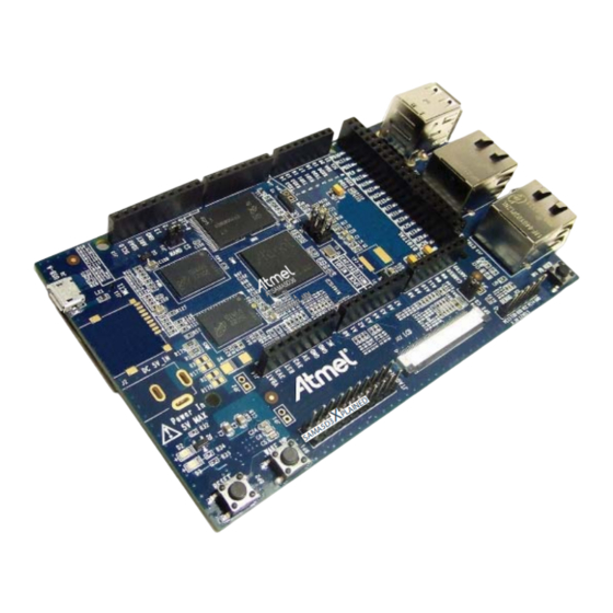
SAMA5D3 XPLAINED Hardware Introduction Introduction The SAMA5D3 Xplained board is a fully-featured evaluation platform for Microchip SAMA5D3 series MPUs. It allows users to extensively evaluate, prototype and create application-specific designs. Equipment List ® The SAMA5D3 Xplained board is built around the integration of a Cortex... -
Page 5: Board Features
On-board power regulation is performed by a Power Management Unit (PMU) Battery On-board optional power Cap for CMOS backup Reset, wake-up and free user push button User interface One red user/power LED and one blue user LED 2019 Microchip Technology Inc. DS50002884A-page 5... - Page 6 SAMA5D3 XPLAINED Board Components Board Overview The full-featured SAMA5D3 Xplained board integrates several peripherals and interface connectors, as shown in Figure 4-1. Figure 4-1: SAMA5D3 Xplained Board Overview J18 PIO Expansion J20 PIO Expansion SPI Interface 2Gb Nand Flash Memory...
- Page 7 SAMA5D3 XPLAINED The SAMA5D3 Xplained board is equipped with the interface connectors described in Table 4-1. Table 4-1: SAMA5D3 Xplained Board Interface Connectors Header Interfaces to Main power supply USB-A device. Supports USB device using a Micro-AB connector J7 (upper) USB-B Host.
-
Page 8: Function Blocks
4.2.1 Processor The SAMA5D3 Xplained board is built around the SAMA5D36, a Cortex-A5 application processor which combines high-performance com- puting device with low-power consumption and a wide range of communication peripherals. It features a combination of user interface functionalities and high data rate IOs, including LCD controller, touchscreen, camera interface, Gigabit and 10/100 Ethernet ports, high- speed USB and SDIO. -
Page 9: Power Supplies
A part of peripheral I/O lines 3.3V VDDUTMII The three USB interfaces 3.3V VDDOSC The main oscillator cells 3.3V VDDANA The analog-to-digital converter The core, including the processor, the 1.2V VDDCORE embedded memories and the peripherals 2019 Microchip Technology Inc. DS50002884A-page 9... - Page 10 100nF VDDOSC OUT7 100nF 100nF 10uH60mA 10uH60mA 2.2uF 2.2uF 2.2uF 2.2uF 2.2uF 2.2uF 2.2uF 2.2uF 4.7uF 4.7uF IRLML2502 IRLML2502 C130 C130 10nF 10nF 100K 1% 100K 1% WAKUP or RESET Force Power ON 2019 Microchip Technology Inc. DS50002884A-page 10...
-
Page 11: Reset Circuitry
4.2.3.1 Power Options Several power options are available to configure the SAMA5D3 Xplained board powering scheme. The power sources are selected by a set of 0R resistors. The USB-powered operation is the default configuration. The power source is the USB device port (J6) connected to a PC or a mini-AB 5V DC supply. -
Page 12: Memory Organization
The memory devices that equip the SAMA5D3 Xplained evaluation kit are as follows: • Two DDR2/SDRAM (MT47H64M16HR) used as main system memory (256 MByte). The board includes 2 Gbits of on-board sol- ®... -
Page 13: Sd/Mmc Interface
4.2.6 SD/MMC Interface The SAMA5D3 Xplained board features two high-speed Multimedia Card Interfaces (MCI). • The first interface is used as an 8-bit interface (MCI0), connected to a SD/MMC card slot (J10) located on the bottom side of the PCB. -
Page 14: Serial Peripheral Interface (Spi)
The SAMA5D3X-series processor features two high-speed Serial Peripheral Interfaces. One port is used to interface with the optional on- board serial DataFlash®. There are four main signals used in the SPI interface; Clock, Data In, Data Out, and Chip Select. 2019 Microchip Technology Inc. DS50002884A-page 14... - Page 15 SAMA5D3 XPLAINED Figure 4-10: Optional Serial DataFlash Schematic VDDIOP1 100K 1% 100K 1% VDDIOP1 PD11 (SPI0_MOSI) PD10 (SPI0_MIS0) C107 C107 PD12 (SPI0_SPCK) 100nF 100nF W/Vpp/DQ2 (SPI0_CS) HOLD/DQ3 PD13 DNP(N25Q032A13ESE40F) DNP(N25Q032A13ESE40F) JUMPER JUMPER 2019 Microchip Technology Inc. DS50002884A-page 15...
- Page 16 SAMA5D3 XPLAINED 4.2.8 Optional 1-Wire EEPROM The SAMA5D3 Xplained board can use a 1-Wire device as “soft label” to store data such as chip type, manufacturer’s name, production date, etc. Figure 4-11: Optional One-Wire EEPROM Schematic VDDIOM 1.5K 1.5K MN11...
- Page 17 Ethernet 10/100 Port The SAMA5D3 Xplained board features a MICREL PHY device (KSZ8081RNB) operating at 10/100 Mb/s. The board supports RMII inter- face modes. The Ethernet interface consists of two pairs of low-voltage differential pair signals designated from GRX± and GTX± plus Control signals for link activity indicators.
-
Page 18: Push Button Switches
SAMA5D3 XPLAINED 4.2.12 The SAMA5D3 Xplained board features three USB communication ports: • Port A: High-speed (EHCI) and full-speed (OHCI) host multiplexed with high-speed USB device Micro-AB connector (J6) • Port B: High-speed (EHCI) and full-speed (OHCI) host, standard type A connector (J7 upper port) •... -
Page 19: Lcd Connector
4.2.15.1 Debug JTAG/ICE A 2x10-pin JTAG header is implemented on the SAMA5D3 Xplained board to enable the software development and debugging of the board by using various JTAG emulators. The interface signals have a voltage level of 3.3V. 2019 Microchip Technology Inc. -
Page 20: Expansion Ports
R171 and R172 are optional (not implemented) resistors that can be used for power selection. Power can be delivered either by the SAMA5D3 Xplained board or by the debug interface tool. To avoid a contention between your debug interface (e.g. FTDI) and the on- board power system, be careful during the installation of one of these resistors. - Page 21 • CAN: CAN-RX0, CANTX0, CANRX1, CAN_TX1 • Analog: AD[0:11], ADTRG, ADREF • GPIO: MISC • RESET • VBAT Refer to the SAMA5D3 series data sheet for further details on the PIO multiplexing and alternate function selection. 2019 Microchip Technology Inc. DS50002884A-page 21...
- Page 22 SAMA5D3 XPLAINED 4.2.16.1 Functions Available Through the Arduino Headers The following tables illustrate the functionalities provided by the SAMA5D3 Xplained board. They show the pins used to implement each functionality. Note: Some pins are multiplexed for different functionalities, which means that only one at a time can be active for each pin.
- Page 23 PA30 TWD0 URXD1 PA31 TWCK0 UTXD1 PC26/PA30 TWD0/TWD1 URXD1 PC27/PA31 TWCK0/TWCK1 URTD1 PC30 UTXD0 PC29 URXD0 PWMFI2 PD14 SCK0 PD15 CTS0 PD18 TXD0 PD17 RXD0 PB25 SCK1 PB26 CTS1 PB29 TXD1 PB28 RXD1 2019 Microchip Technology Inc. DS50002884A-page 23...
- Page 24 GPIO PC24/PC0 GPIO GPIO GPIO PE10 GPIO PE11 GPIO PE12 GPIO PE16 GPIO PE31 IRQ/PWML1 PC28 PWMFI0 PA20 PWMH0 PA22 PWMH1 PA21 PWML0 PA23 PWML1 PE29 TCLK2 TCLK4 TCLK5 TIOA4 TIOA5 TIOB4 TIOB5 2019 Microchip Technology Inc. DS50002884A-page 24...
- Page 25 Function 4 Function 5 SCL0 PA31 TWCK0 UTXD1 ISI_HSYNC SDA0 PA30 TWD0 URXD1 ISI_VSYNC ARFE PC24 SPI1_SPCK ETX0 TIOA3 PC22 SPI1_MISO ETX1 TIOB3 PC23 SPI1_MOSI ERX0 TCLK3 PC25 SPI1_NPCS0 ERX1 TIOA4 ETXEN TIOB4 2019 Microchip Technology Inc. DS50002884A-page 25...
- Page 26 J18 Header Table 4-8: J18 Header IOs Silkscreen Function 1 Function 2 Function 3 ECRSDV TCLK4 ERXER TIOA5 EREFCK TIOB5 PC28 SPI1_NPCS3 PWMFI0 ISI_D9 EMDC TCLK5 EMDIO PC30 UTXD0 ISI_PCK PC29 URXD0 PWMFI2 ISI_D8 2019 Microchip Technology Inc. DS50002884A-page 26...
- Page 27 TXD1 RXD1 17 PB28 RXD1 TXD0 18 PD18 TXD0 RXD0 19 PD17 RXD0 SDA 20 PC26 SPI1_NPCS1 TXWD1 ISI_D11 PA30 TWD0 URXD1 ISI_VSYNC SCL 21 PC27 SPI1_NPCS2 TWCK1 ISI_D10 PA31 TWCK0 UTXD1 ISI_HSYNC 2019 Microchip Technology Inc. DS50002884A-page 27...
- Page 28 PA17 PA17 LCDDAT17 ISI_D1 PA19 PA19 LCDDAT19 TWCk2 ISI_D3 PA21 PA21 LCDDAT21 PWML0 ISI_D5 PA23 PA23 LCDDAT23 PWML1 ISI_D7 PE15 PE15 SCK3 PE17 PE17 RTS3 PE11 PE11 PE23 PE23 CTS2 PE25 PE25 RXD2 2019 Microchip Technology Inc. DS50002884A-page 28...
- Page 29 PA20 LCDDAT20 PWMH0 ISI_D4 PA22 PA22 LCDDAT22 PWMH1 ISI_D6 PE16 PE16 CTS3 PE20 PE20 SCK2 PE12 PE12 PE24 PE24 RTS2 PE26 PE26 NCS0 TXD2 PE14 PE14 PE31 PE31 PWML1 PB15 PB15 GCOL CANTX1 2019 Microchip Technology Inc. DS50002884A-page 29...
- Page 30 SAMA5D3 XPLAINED 4.2.16.6 J16 Header Figure 4-24: J16 Header Table 4-11: J16 Header IOs Silkscreen Function 1 MISO1 PC22 SPI1_MISO 5V/3V3 Power supply SPCK PC24 SPI1_SPCK MOSI1 PC23 SPI1_MOSI NRST System reset Power ground 2019 Microchip Technology Inc. DS50002884A-page 30...
- Page 31 Main 3.3V supply - generated by the on-board regulator. Maximum sourced current is 1.2A. This regulator also provides the power supply to the SAMA5D36 microcontroller and components. Main 5.0V supply System ground System ground Not connected 2019 Microchip Technology Inc. DS50002884A-page 31...
- Page 32 SAMA5D3 XPLAINED 4.2.16.8 J17 Header Figure 4-26: J17 Header Table 4-13: J17 Header IOs Silkscreen Function 1 Function 2 Function 3 Function 4 Function 5 PC18 PD20 PD21 PD22 PD23 PD24 PD25 PD26 PD27 2019 Microchip Technology Inc. DS50002884A-page 32...
- Page 33 Function 3 Function 4 Function 5 PC20 PD28 PC21 PD29 PC19 PD30 AD10 PCK0 PD31 PCK1 PB14 GCRS CANRX1 PD19 ADTRG PB15 GCOL CANTX1 CANRX0 PD14 SCK0 SPO_NPCS1 CANRX0 CANTX0 PD15 CTS0 SPI0_NPCS2 CANTX0 2019 Microchip Technology Inc. DS50002884A-page 33...
-
Page 34: Jtag/Ice Connector
JTAG port. Typically connected to nTRST on the target CPU. This pin is Output signal that resets the target. normally pulled high on the target to avoid unintentional resets when there is no connection. Common ground. 2019 Microchip Technology Inc. DS50002884A-page 34... -
Page 35: Signal Description
Active-Low Reset signal. Target CPU Reset signal. Common ground This pin is not connected. Common ground This pin is not connected. Common ground 4.3.3 USB Type-A Dual Port Figure 4-30: USB Type-A Dual Port J19 2019 Microchip Technology Inc. DS50002884A-page 35... - Page 36 USB Host/Device Micro-AB Connector J6 1 2 3 4 5 Table 4-18: USB Device Micro-AB Connector J6 Signal Descriptions Mnemonic Signal Description Vbus 5V power Data minus Data plus On-the-go identification Common ground 2019 Microchip Technology Inc. DS50002884A-page 36...
-
Page 37: Debug Connector
Command line Command line Supply voltage 3.3V Clock / command line Card detect DAT0 Data bit DAT1 Data bit DAT2 Data bit DAT4 Data bit DAT5 Data bit DAT6 Data bit DAT7 Data bit 2019 Microchip Technology Inc. DS50002884A-page 37... - Page 38 Data bit 1 Not used, grounded CARD DETECT Card detect 4.3.8 Gigabit Ethernet ETH0 RJ45 Socket J12 Figure 4-35: Gigabit Ethernet RJ45 Socket J12 1 2 3 4 5 6 7 8 RJ-45 2019 Microchip Technology Inc. DS50002884A-page 38...
- Page 39 Data line Data line Data line Data line Data line Data line Data line Data line Data line Data line Data line Data line Data line Data line Data line Data line Data line 2019 Microchip Technology Inc. DS50002884A-page 39...
- Page 40 RESET Reset for both display and maXTouch Reset for both display and maXTouch 3.3V or 5V supply (0R) 3.3V supply 3.3V or 5V supply (0R) 3.3V supply Note 1: See Section 5. “Errata”. 2019 Microchip Technology Inc. DS50002884A-page 40...
- Page 41 LCDHSYNC – – – LCDHSYNC VDDIOP0 PA28 LCDPCK – – – LCDPCK VDDIOP0 PA29 LCDDEN – – – LCDDEN ISI_VSYN VDDIOP0 PA30 TWD0 URXD1 TWD0 URXD1/ISI_VSYNC ISI_HSYN VDDIOP0 PA31 TWCK0 UTXD1 TWCK0 UTXD1/ISI_HSYNC 2019 Microchip Technology Inc. DS50002884A-page 41...
- Page 42 RTS1 PWMH1 – – RTS1 VDDIOP1 PB28 RXD1 – – – RXD1 VDDIOP1 PB29 TXD1 – – – TXD1 VDDIOP0 PB30 DRXD – – DRXD (DBGU) VDDIOP0 PB31 DTXD – – DTXD (DBGU) 2019 Microchip Technology Inc. DS50002884A-page 42...
- Page 43 PC27 SPI1_NPCS2 TWCK1 ISI_D10 – SPI1_NPCS2/TWCK1 VDDIOP0 PC28 SPI1_NPCS3 PWMFI0 ISI_D9 – SPI1_NPCS3/ISI_D9 VDDIOP0 PC29 URXD0 PWMFI2 ISI_D8 – URXD0/ISI_D8 VDDIOP0 PC30 UTXD0 ISI_PCK – – UTXD0/ISI_PCK VDDIOP0 PC31 PWMFI1 – IRQ_PMIC – 2019 Microchip Technology Inc. DS50002884A-page 43...
- Page 44 VDDANA PD26 – – – VDDANA PD27 – – – VDDANA PD28 – – – VDDANA PD29 – – – VDDANA PD30 AD10 PCK0 – AD10/PCK0 VDDANA PD31 AD11 PCK1 – – AD11/PCK1 2019 Microchip Technology Inc. DS50002884A-page 44...
- Page 45 VDDIOM PE27 NCS1 TIOA2 LCDDAT22 – LCDDAT22 VDDIOM PE28 NCS2 TIOB2 LCDDAT23 LCDDAT23 VDDIOM PE29 NWR1/NBS1 TCLK2 – USER_PB NWR1/NBS1/TCLK2 VDDIOM PE30 NWAIT – – nPBSTA_PMIC – VDDIOM PE31 PWML1 – – IRQ/PWML1 2019 Microchip Technology Inc. DS50002884A-page 45...
- Page 46 SAMA5D3 XPLAINED SAMA5D3 Xplained Board Schematics This section contains the following schematics: • General information • Block Diagram • PIO Multiplexing Table • Power Supplies • SAMA5D3 Device and USB Interfaces • DDR2 Memory • NAND Flash and Optional Memories •...
- Page 47 SAMA5D3 XPLAINED Figure 4-38: General information 2019 Microchip Technology Inc. DS50002884A-page 47...
-
Page 48: Block Diagram
SAMA5D3 XPLAINED Figure 4-39: Block Diagram Extension board connectors 2019 Microchip Technology Inc. DS50002884A-page 48... - Page 49 SAMA5D3 XPLAINED Figure 4-40: PIO Multiplexing Table 2019 Microchip Technology Inc. DS50002884A-page 49...
- Page 50 SAMA5D3 XPLAINED Figure 4-41: Power Supplies 2019 Microchip Technology Inc. DS50002884A-page 50...
- Page 51 SAMA5D3 XPLAINED Figure 4-42: SAMA5D3 Device and USB Interfaces 2019 Microchip Technology Inc. DS50002884A-page 51...
- Page 52 SAMA5D3 XPLAINED Figure 4-43: DDR2 Memory 2019 Microchip Technology Inc. DS50002884A-page 52...
- Page 53 SAMA5D3 XPLAINED Figure 4-44: NAND Flash and Optional Memories 2019 Microchip Technology Inc. DS50002884A-page 53...
- Page 54 SAMA5D3 XPLAINED Figure 4-45: SD and Micro-SD Interfaces 2019 Microchip Technology Inc. DS50002884A-page 54...
- Page 55 SAMA5D3 XPLAINED Figure 4-46: Gigabit Ethernet 2019 Microchip Technology Inc. DS50002884A-page 55...
- Page 56 SAMA5D3 XPLAINED Figure 4-47: Ethernet 10/100 2019 Microchip Technology Inc. DS50002884A-page 56...
- Page 57 SAMA5D3 XPLAINED Figure 4-48: LCD, JTAG, DEBUG and Extended Connectors 2019 Microchip Technology Inc. DS50002884A-page 57...
- Page 58 Unsolder and remove resistors R96, R97, R101 and Solder isolated pieces of wire as follows. R103 located here: Resin coated wires were used below. Make sure not to create any short-circuits between the wires and the other components. 2019 Microchip Technology Inc. DS50002884A-page 58...
- Page 59 JP1 routing is incorrect and results in inaccurate VDDCORE current measurement The jumper JP1 was incorrectly routed on the SAMA5D3 Xplained board. As a result, the on-board connections on the left and right sides of the jumper do not match the schematics and VDDCORE current measurement is incorrect.
- Page 60 On the bottom side, cut the large track between C13 and L7. Before After Zoom Unsolder C13 and re-solder it across the cut made in Step 3, directly to L7. C13 Removed C13 Re-soldered 2019 Microchip Technology Inc. DS50002884A-page 60...
- Page 61 Although the board proves to be functional as is, we recommend fixing this excessive pull-up charge by removing resistors R178 and R179. These are located near the J17 connector and an Atmel logo, as shown in the following figure: Figure 5-1: Position of R178 and R179 2019 Microchip Technology Inc. DS50002884A-page 61...
-
Page 62: Revision History
SAMA5D3 XPLAINED Revision History Table 6-1: SAMA5D3 Xplained User Guide Revision History Doc. Rev. Changes Section 4.2.3 “Power Supplies”: added Warning on engineering version. General - Template update: Moved from Atmel to Microchip template. DS50002884A - The user’s guide is assigned a new document number (DS50002884) and revision letter is reset to A. -
Page 63: The Microchip Web Site
Customers should contact their distributor, representative or Field Application Engineer (FAE) for support. Local sales offices are also available to help customers. A listing of sales offices and locations is included in the back of this document. Technical support is available through the web site at: http://microchip.com/support 2019 Microchip Technology Inc. DS50002884A-page 63... -
Page 64: Microchip Devices Code Protection Feature
SQTP is a service mark of Microchip Technology Incorporated in the U.S.A. Silicon Storage Technology is a registered trademark of Microchip Technology Inc. in other countries. GestIC is a registered trademark of Microchip Technology Germany II GmbH & Co. KG, a subsidiary of Microchip Technology Inc., in other countries. -
Page 65: Quality Management System Certified By Dnv
PIC® MCUs and dsPIC® DSCs, KEELOQ® code hopping devices, Serial EEPROMs, microperipherals, nonvolatile memory and analog products. In addition, Microchip’s quality system for the design and manufacture of development systems is ISO 9001:2000 certified. 2019 Microchip Technology Inc. DS50002884A-page 65... -
Page 66: Worldwide Sales And Service
New York, NY Tel: 46-31-704-60-40 Tel: 631-435-6000 Sweden - Stockholm San Jose, CA Tel: 46-8-5090-4654 Tel: 408-735-9110 UK - Wokingham Tel: 408-436-4270 Tel: 44-118-921-5800 Fax: 44-118-921-5820 Canada - Toronto Tel: 905-695-1980 Fax: 905-695-2078 2019 Microchip Technology Inc. DS50002884A-page 66...
Need help?
Do you have a question about the SAMA5D3 XPLAINED and is the answer not in the manual?
Questions and answers