Table of Contents
Advertisement
Quick Links
Evaluating the ADN4693E-1 3.3 V, 200 Mbps, Full-Duplex, High Speed M-LVDS Transceiver
FEATURES
Easy evaluation of the
ADN4693E-1
►
LVDS transceiver
Board layout optimized for high speed signaling
►
Matched track lengths on M-LVDS differential pairs with control-
►
led 100 Ω differential impedance
Matched track lengths on high speed DI and RO logic signals
►
with controlled 50 Ω impedance to GND
SMA jacks for connecting to high speed DI and RO logic signals
►
and the M-LVDS A, B, Y, and Z signals
Optional screw terminal connectors for accessing the RO, RE,
►
DE, and DI logic signals
Power and ground connections through screw terminal blocks
►
Jumper-selectable driver enable and receiver enable via the RE
►
and DE pins
Test points for measuring all signals and multiple ground points
►
to facilitate probing of multiple signals
100 Ω termination resistors across A and B signals and Y and Z
►
signals to simulate a terminated bus
EQUIPMENT NEEDED
A 4 channel oscilloscope
►
A signal generator
►
A 3.0 V to 3.6 V power supply
►
EVALUATION KIT CONTENTS
EVAL-ADN4693E-1EBZ
►
PLEASE SEE THE LAST PAGE FOR AN IMPORTANT
WARNING AND LEGAL TERMS AND CONDITIONS.
200 Mbps, full-duplex, M-
User Guide | EVAL-ADN4693E-1
GENERAL DESCRIPTION
The EVAL-ADN4693E-1EBZ allows quick and easy evaluation
of the ADN4693E-1 200 Mbps, full-duplex, multipoint, low
voltage differential signaling (M-LVDS) transceiver. The EVAL-
ADN4693E-1EBZ allows the input and output functions of the trans-
ceiver to be exercised without the need for external components.
Subminiature A (SMA) connectors provide convenient connections
for high speed logic and the M-LVDS bus signals. Screw terminal
blocks are available to access power, ground, and digital signals.
Jumper options allow control of the driver and receiver enable pins
of the transceiver.
The EVAL-ADN4693E-1EBZ is optimized for high speed signal-
ing. The differential M-LVDS signal traces on the board are
routed as length matched 100 Ω differential pairs. The EVAL-
ADN4693E-1EBZ features a solid ground and power plane for
optimum power integrity.
The EVAL-ADN4693E-1EBZ has a footprint for the ADN4693E-1
full-duplex transceiver in a 4 mm × 4 mm, 16-lead, lead frame chip
scale package (LFCSP).
For full details on the ADN4693E-1, see the ADN4693E-1 data
sheet, which must be used in conjunction with this user guide when
using the EVAL-ADN4693E-1EBZ.
UG-1924
Rev. 0 | 1 of 9
Advertisement
Table of Contents

Subscribe to Our Youtube Channel
Related Manuals for Analog Devices EVAL-ADN4693E-1


Summary of Contents for Analog Devices EVAL-ADN4693E-1
-
Page 1: Features
User Guide | EVAL-ADN4693E-1 UG-1924 Evaluating the ADN4693E-1 3.3 V, 200 Mbps, Full-Duplex, High Speed M-LVDS Transceiver FEATURES GENERAL DESCRIPTION Easy evaluation of the ADN4693E-1 200 Mbps, full-duplex, M- The EVAL-ADN4693E-1EBZ allows quick and easy evaluation ► LVDS transceiver of the ADN4693E-1 200 Mbps, full-duplex, multipoint, low voltage differential signaling (M-LVDS) transceiver. -
Page 2: Table Of Contents
User Guide EVAL-ADN4693E-1 TABLE OF CONTENTS Features..............1 Setting Up the Evaluation Board......4 Equipment Needed..........1 Input and Output Connections......5 Evaluation Kit Contents......... 1 Jumper Connections.......... 5 General Description..........1 Evaluation Board Schematic and Layout....6 EVAL-ADN4693E-1EBZ Evaluation Board Ordering Information..........9 Photograph............3 Bill of Materials........... -
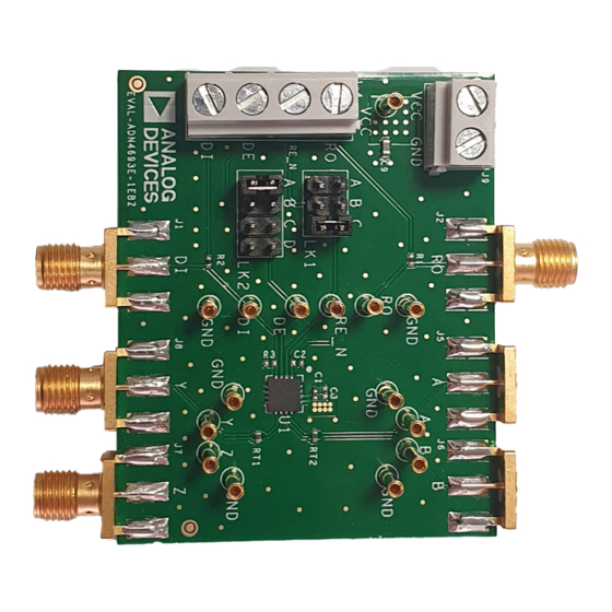
Page 3: Eval-Adn4693E-1Ebz Evaluation Board Photograph
User Guide EVAL-ADN4693E-1 EVAL-ADN4693E-1EBZ EVALUATION BOARD PHOTOGRAPH Figure 1. analog.com Rev. 0 | 3 of 9... -
Page 4: Evaluation Board Configuration
User Guide EVAL-ADN4693E-1 EVALUATION BOARD CONFIGURATION wire connections to a microprocessor. The connections to the J1-4 SETTING UP THE EVALUATION BOARD screw terminal block are made via 0 Ω resistors, which can be The EVAL-ADN4693E-1EBZ allows the ADN4693E-1 to be quickly removed to eliminate any stub lengths along the interconnect. -
Page 5: Input And Output Connections
User Guide EVAL-ADN4693E-1 EVALUATION BOARD CONFIGURATION INPUT AND OUTPUT CONNECTIONS Table 1 details the digital input and output connections, and Table 2 details the M-LVDS input and output connections. Table 1. Digital I/O Connections Connection SMA Connector Terminal Connector J1-4 via R2... -
Page 6: Evaluation Board Schematic And Layout
User Guide EVAL-ADN4693E-1 EVALUATION BOARD SCHEMATIC AND LAYOUT Figure 3. EVAL-ADN4693E-1EBZ Schematic analog.com Rev. 0 | 6 of 9... - Page 7 User Guide EVAL-ADN4693E-1 EVALUATION BOARD SCHEMATIC AND LAYOUT Figure 4. EVAL-ADN4693E-1EBZ Silkscreen Figure 6. EVAL-ADN4693E-1EBZ Internal Layer 2 (GND) Figure 7. EVAL-ADN4693E-1EBZ Internal Layer 3 (VCC) Figure 5. EVAL-ADN4693E-1EBZ Component Side analog.com Rev. 0 | 7 of 9...
- Page 8 User Guide EVAL-ADN4693E-1 EVALUATION BOARD SCHEMATIC AND LAYOUT Figure 8. EVAL-ADN4693E-1EBZ Solder Side analog.com Rev. 0 | 8 of 9...
-
Page 9: Ordering Information
Evaluation Board until you have read and agreed to the Agreement. Your use of the Evaluation Board shall signify your acceptance of the Agreement. This Agreement is made by and between you (“Customer”) and Analog Devices, Inc. (“ADI”), with its principal place of business at Subject to the terms and conditions of the Agreement, ADI hereby grants to Customer a free, limited, personal, temporary, non-exclusive, non-sublicensable, non-transferable license to use the Evaluation Board FOR EVALUATION PURPOSES ONLY.
Need help?
Do you have a question about the EVAL-ADN4693E-1 and is the answer not in the manual?
Questions and answers