
Subscribe to Our Youtube Channel
Related Manuals for Alinx AXKU15


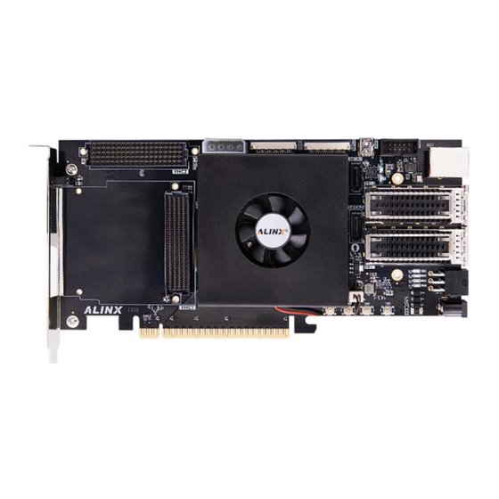
Summary of Contents for Alinx AXKU15
- Page 1 Xilinx FPGA Development Platform User Manual AXKU15 Development Board ALINX ELECTRONIC LIMITED WWW.EN.ALINX.COM...
-
Page 2: Version Record
AXKU15 User Manual Version Record Version Date Release By Description Rev 1.0 2024/3/22 Kathy Xia First Release www.en.alinx.com 2/51 www.en.alinx.com... -
Page 3: Table Of Contents
AXKU15 User Manual Table of Contents Version Record ..........................2 Part 1: Development Board Introduction ................... 5 Part 2: ACKU15 SOM Module ......................7 Part 2.1: Introduction ....................... 7 Part 2.2: FPGA Chip........................7 Part 2.3: DDR4 ........................... 9 Part 2.4: QSPI Flash ....................... 13 Part 2.5: Clock Configuration ..................... - Page 4 AXKU15 User Manual The development board (model: AXKU15) based on the Xilinx FPGA Kintex Ultrascale+ development platform of Alinx Electronic Technology has been officially released. To let users have a quick understanding of this development platform, we have written this user manual.
-
Page 5: Part 1: Development Board Introduction
AXKU15 User Manual Part 1: Development Board Introduction Here is a brief introduction to the functionality of the Kintex Ultrascale+ AXKU15 development platform. The whole structure of the development board is designed by inheriting our consistent SOM module + expansion board model. - Page 6 AXKU15 User Manual PCIe3.0 x16 interface ⚫ It supports PCI Express 3.0 standard, provides standard PCIe x16 high-speed data transmission interface, and the communication rate of single channel can be up to 8GBaud. 2 * FMC HPC interface ⚫ Eight high-speed transceivers in the FPGA are connected to high-speed pins dedicated for the FMC HPC, wherein one FMC interface leads out 34 pairs of LA signal differential pairs, 2 pairs of clock signals and 24 pairs of HA signals;...
-
Page 7: Part 2: Acku15 Som Module
AXKU15 User Manual Part 2: ACKU15 SOM Module Part 2.1: Introduction ACKU15 (SOM model, the same below) SOM module, FPGA chip is based on the Xilinx FPGA Kintex Ultrascale+ main chip XCKU15PFFVE1517 design. The module connects five DDR4 memory chips to the HP port of the FPGA to form an 80-bit data bandwidth, and the capacity of each DDR4 chip is up to 1GB. - Page 8 AXKU15 User Manual Figure 4: Ordering Information Figure 5 is the physical picture of the FPGA chip used in the development board. Figure 5: Physical FPGA chip The main parameters of the FPGA chip are as follows: Name Specific parameters...
-
Page 9: Part 2.3: Ddr4
AXKU15 User Manual Part 2.3: DDR4 The ACKU15 SOM module is equipped with five Micron 1GB DDR4 chips, model MT40A512M16LY-062 E, which are connected to the HP side of the FPGA to form an 80-bit data bus with a capacity of 5GB. The maximum running data rate of DDR4 SDRAM on the FPGA side is 2,666Mbps, and five DDR4 memory systems are directly connected to the memory interfaces of BANK 66, 67 and 68. - Page 10 AXKU15 User Manual DDR4 SDRAM pin assignment: Signal name Pin number DDR4_D0 AJ28 DDR4_D1 AK27 DDR4_D2 AK26 DDR4_D3 AL27 DDR4_D4 AJ26 DDR4_D5 AN26 DDR4_D6 AN27 DDR4_D7 AK28 DDR4_D8 AK22 DDR4_D9 AL24 DDR4_D10 AJ23 DDR4_D11 AM25 DDR4_D12 AH23 DDR4_D13 AK24 DDR4_D14...
- Page 11 AXKU15 User Manual DDR4_D46 AJ33 DDR4_D47 AJ34 DDR4_D48 AK32 DDR4_D49 AL32 DDR4_D50 AJ30 DDR4_D51 AM33 DDR4_D52 AH31 DDR4_D53 AH32 DDR4_D54 AJ29 DDR4_D55 AM32 DDR4_D56 AL29 DDR4_D57 AM30 DDR4_D58 AM29 DDR4_D59 AN33 DDR4_D60 AP28 DDR4_D61 AL30 DDR4_D62 AP29 DDR4_D63 AN32 DDR4_D64...
- Page 12 AXKU15 User Manual DDR4_DQS2_N AR27 DDR4_DQS2_P AR26 DDR4_DQS3_N AV25 DDR4_DQS3_P AU25 DDR4_DQS4_N AK38 DDR4_DQS4_P AK37 DDR4_DQS5_N AN36 DDR4_DQS5_P AN35 DDR4_DQS6_N AL31 DDR4_DQS6_P AK31 DDR4_DQS7_N AN31 DDR4_DQS7_P AN30 DDR4_DQS8_N AW30 DDR4_DQS8_P AV30 DDR4_DQS9_N AV33 DDR4_DQS9_P AV32 DDR4_OTD AR33 DDR4_PAR AV36 DDR4_RAS_B...
-
Page 13: Part 2.4: Qspi Flash
AXKU15 User Manual Part 2.4: QSPI Flash The module is equipped with two Quad-SPI FLASH chips of 512MBit size, model MT25QU512ABA1EW9, which uses 1.8V CMOS voltage standard. Due to the non-volatile nature of QSPI FLASH, it can store the configuration Bin file of the FPGA as well as other user data files during use. -
Page 14: Part 2.5: Clock Configuration
AXKU15 User Manual Part 2.5: Clock Configuration The module provides two 200Mhz differential active clocks for the FPGA system. And provide differential clock sources for that logic part of the FPGA respectively. The schematic diagram of the clock circuit design is shown in... -
Page 15: Part 2.6: Led Light
AXKU15 User Manual Figure 11: System clock source Figure 12: System clock source Clock pin assignment: Signal name FPGA pins B94_L5_P B94_L5_N DDR4_CLKREF_P AR32 DDR4_CLKREF_N AT32 Table 6: Clock pin assignments Part 2.6: LED Light There are three red LEDs on the ACKU15 module, one of which is a power indicator (PWR1), one of which is a configuration LED (D1), and a user indicator (LED 1). -
Page 16: Part 2.7: Power Source
AXKU15 User Manual Figure 13: Schematic diagram of hardware connection of LED lamp on module Part 2.7: Power source The power supply voltage of the ACKU15 module is +12V, which is supplied through the connection base board. The power supply design diagram on the board is shown in Figure 14 below: Figure 14: Power interface part in the schematic diagram www.en.alinx.com... -
Page 17: Part 2.8: Structure Diagram
AXKU15 User Manual The +12V generates the FPGA core power supply through the DCDC power supply chip IS6608, and the output current is up to 60A, which can meet the current demand of the core voltage. The +12V power supply supplies power to the FPGA auxiliary power supply and the high-speed transceiver through three DCDC chips: SGM61163 generates VCCAUX, and IS66066 generates MGTAVCC and MGTAVTT power supplies. - Page 18 AXKU15 User Manual Pin Assignments for J1 Connector: J1 pin Signal name FPGA pin number J1 pin Signal name FPGA pin number B90_L10_N B90_L12_N B90_L10_P B90_L12_P B90_L8_N B90_L11_N B90_L8_P B90_L11_P B90_L9_N B90_L7_N B90_L9_P B90_L7_P B90_L4_N B90_L6_N B90_L4_P B90_L6_P B90_L5_N B90_L3_N...
- Page 19 AXKU15 User Manual MGT227_CLK0_P AE12 MGT227_CLK1_P AD10 MGT227_CLK0_N AE11 MGT227_CLK1_N MGT227_RX3_P MGT227_TX3_P MGT227_RX3_N MGT227_TX3_N MGT227_RX2_P MGT227_TX2_P MGT227_RX2_N MGT227_TX2_N MGT227_RX1_P MGT227_TX1_P MGT227_RX1_N MGT227_TX1_N MGT227_RX0_P MGT227_TX0_P MGT227_RX0_N MGT227_TX0_N Table 7: Pin Assignments for J1 Connector J1 pin Signal name FPGA pin number...
- Page 20 AXKU15 User Manual MGT229_RX3_P MGT229_TX3_P MGT229_RX3_N MGT229_TX3_N MGT229_RX2_P MGT229_TX2_P MGT229_RX2_N MGT229_TX2_N MGT229_RX1_P MGT229_TX1_P MGT229_RX1_N MGT229_TX1_N MGT229_RX0_P MGT229_TX0_P MGT229_RX0_N MGT229_TX0_N MGT229_CLK1_P MGT229_CLK0_P AA12 MGT229_CLK1_N MGT229_CLK0_N AA11 MGT228_RX3_P MGT228_TX3_P MGT228_RX3_N MGT228_TX3_N MGT228_RX2_P MGT228_TX2_P MGT228_RX2_N MGT228_TX2_N MGT228_RX1_P MGT228_TX1_P MGT228_RX1_N MGT228_TX1_N MGT228_RX0_P MGT228_TX0_P MGT228_RX0_N...
- Page 21 AXKU15 User Manual B65_L18_N AL16 B65_L16_N AL17 B65_L20_P AN13 B65_L14_P AM15 B65_L20_N AP13 B65_L14_N AN15 B65_L11_P AR14 B65_L10_P AP16 B65_L11_N AT14 B65_L10_N AR16 B65_L7_P AV16 B65_L8_P AT15 B65_L7_N AW16 B65_L8_N AU15 B65_L9_P AV15 B65_L6_P AU14 B65_L9_N AW15 B65_L6_N AU13 VCCIO_64 AK20、AN19、AT8...
- Page 22 AXKU15 User Manual J2 pin Signal name FPGA pin number J2 pin Signal name FPGA pin number FPGA_TMS AD22 B64_L9_P AP21 FPGA_TCK AG23 B64_L9_N AP20 B64_L5_P AT22 B64_L7_P AR22 B64_L5_N AT21 B64_L7_N AR21 B64_L3_P AV21 B64_L15_P AT20 B64_L3_N AW21 B64_L15_N...
- Page 23 AXKU15 User Manual MGT226_CLK0_P AG12 MGT226_CLK1_P AF10 MGT226_CLK0_N AG11 MGT226_CLK1_N MGT226_RX0_P MGT226_TX0_P MGT226_RX0_N MGT226_TX0_N MGT226_RX1_P MGT226_TX1_P MGT226_RX1_N MGT226_TX1_N MGT226_RX2_P MGT226_TX2_P MGT226_RX2_N MGT226_TX2_N MGT226_RX3_P MGT226_TX3_P MGT226_RX3_N MGT226_TX3_N Table 10: Pin Assignments for J2 Connector Pin assignment for J3 connector: J3 pin...
- Page 24 AXKU15 User Manual MGT129_RX1_N MGT129_TX1_N MGT129_RX0_P MGT129_TX0_P MGT129_RX0_N MGT129_TX0_N MGT129_CLK0_P MGT129_CLK1_P MGT129_CLK0_N MGT129_CLK1_N MGT127_CLK0_P AE29 MGT127_CLK1_P AC29 MGT127_CLK0_N AE30 MGT127_CLK1_N AC30 MGT127_RX3_P AE38 MGT127_TX3_P AC33 MGT127_RX3_N AE39 MGT127_TX3_N AC34 MGT127_RX2_P AF36 MGT127_TX2_P AD31 MGT127_RX2_N AF37 MGT127_TX2_N AD32 MGT127_RX1_P AG38 MGT127_TX1_P...
- Page 25 AXKU15 User Manual MGT132_RX1_N MGT132_TX0_P MGT132_RX0_P MGT132_TX0_N MGT132_RX0_N MGT132_CLK1_P MGT132_CLK0_P MGT132_CLK1_N MGT132_CLK0_N MGT130_TX3_P MGT130_RX3_P MGT130_TX3_N MGT130_RX3_N MGT130_TX2_P MGT130_RX2_P MGT130_TX2_N MGT130_RX2_N MGT130_TX1_P MGT130_RX1_P MGT130_TX1_N MGT130_RX1_N MGT130_TX0_P MGT130_RX0_P MGT130_TX0_N MGT130_RX0_N MGT130_CLK1_P MGT130_CLK0_P MGT130_CLK1_N MGT130_CLK0_N MGT128_CLK1_P AA29 MGT128_CLK0_P AB27 MGT128_CLK1_N AA30 MGT128_CLK0_N AB28...
- Page 26 AXKU15 User Manual Pin assignments for the J4 connector: J4 pin Signal name FPGA pin number J4 pin Signal name FPGA pin number E2、 F5、 B8、 F10、 K12、 VCCO_90_91_93_94 POWER_SCL N11、B13、G13 B94_L9_N B94_L6_N B94_L9_P B94_L6_P B94_L8_N B94_L7_N B94_L8_P B94_L7_P B71_L1_N...
- Page 27 AXKU15 User Manual B69_L3_N B69_L1_N B69_L3_P B69_L1_P B69_L5_N B69_L4_N B69_L5_P B69_L4_P B69_L2_N B69_L11_N B69_L2_P B69_L11_P B69_L24_N B69_L9_N B69_L24_P B69_L9_P B69_L16_N B69_L8_N B69_L16_P B69_L8_P B69_L15_N B69_L7_N B69_L15_P B69_L7_P Table 13: Pin Assignments for J4 Connector J4 pin Signal name FPGA pin number...
- Page 28 AXKU15 User Manual B71_L2_N B71_L15_N B71_L2_P B71_L15_P B70_L10_N B70_L21_N B70_L10_P B70_L21_P B70_L12_N B70_L22_N B70_L12_P B70_L22_P B70_L24_N B70_L5_N B70_L24_P B70_L5_P B70_L19_N B70_L23_N B70_L19_P B70_L23_P B69_L6_N B69_L13_N B69_L6_P B69_L13_P B69_L17_N B69_L14_N B69_L17_P B69_L14_P B69_L18_N B69_L22_N B69_L18_P B69_L22_P B69_L20_N B69_L19_N B69_L20_P B69_L19_P B69_L12_N...
-
Page 29: Part 3: Base Board
⚫ Part 3.2: PCIe Slot There is a PCIe x16 interface on the AXKU15 base board, which supports PCIe Gen3.0 protocol, and 8 pairs of transceivers are connected to the golden finger of PCIEx16 for data communication. The receiving and transmitting signals of the PCIe interface are directly connected to the FPGA BANK228 ~ 231 transceivers. - Page 30 AXKU15 User Manual Figure 16: Schematic Diagram of PCIe Slot Design The PCIe x16 interface FPGA pin assignments are as follows: Signal name FPGA pin name Pin number Remark PCIE_RX0_P MGT231_RX3_P PCIE channel 0 data receiving positive PCIE_RX0_N MGT231_RX3_N PCIE Channel 0 Data Receive Negative...
-
Page 31: Part 3.3: Gigabit Network Interface
AXKU15 User Manual PCIE_RX12_N MGT228_RX3_N PCIE channel 12 data transmission negative PCIE_RX13_P MGT228_RX2_P PCIE Channel 13 Data Sending Positive PCIE_RX13_N MGT228_RX2_N PCIE channel 13 data transmission negative PCIE_RX14_P MGT228_RX1_P PCIE Channel 14 Data Sending Positive PCIE_RX14_N MGT228_RX1_N PCIE channel 14 data transmission negative... - Page 32 AXKU15 User Manual network transmission rate and communicates with FPGA through RGMII interface. JL21221D chip supports MDI/MDX self-adaptation, various speed self-adaptation and Master/Slave self-adaptation and supports register management of PHY by MDIO bus. When the JL21221D is powered on, it will detect the level status of some specific IOs to determine its own working mode.
-
Page 33: Part 3.4: Fmc Hpc Interface
The development board is equipped with two FMC HPC expansion ports, namely FMC1 (J12) and FMC2 (J13), which can be externally connected with XILINX or various FMC modules of Alinx (HDMI input and output module, binocular camera module, high-speed AD module, etc.). - Page 34 AXKU15 User Manual The FMC HPC J12 connector pin assignments are as follows: Signal name FPGA pin name FPGA pin number Remark FMC1_CLK0_N B70_L11_N FMC channel 0 input reference clock N FMC1_CLK0_P B70_L11_P FMC channel 0 input reference clock P...
- Page 35 AXKU15 User Manual FMC1_LA20_N B69_L17_N FMC LA Channel 20 Data N FMC1_LA20_P B69_L17_P FMC LA Channel 20 Data P FMC1_LA21_N B69_L2_N FMC LA Channel 21 Data N FMC1_LA21_P B69_L2_P FMC LA 21th data P FMC1_LA22_N B69_L4_N FMC LA Channel 22 Data N...
- Page 36 AXKU15 User Manual FMC1_HA09_N B71_L17_N FMC HA Channel 9 Data N FMC1_HA09_P B71_L17_P FMC HA Channel 9 Data P FMC1_HA10_N B71_L8_N FMC HA 10th Channel Data N FMC1_HA10_P B71_L8_P FMC HA Channel 10 Data P FMC1_HA11_N B71_L16_N FMC HA Channel 11 Data N...
- Page 37 AXKU15 User Manual FMC1_DP6_M2C_P MGT227_RX2_P Transceiver Data 6 Input P FMC1_DP6_M2C_N MGT227_RX2_N Transceiver Data 6 Input N FMC1_DP7_M2C_P MGT227_RX3_P Transceiver Data 7 Input P FMC1_DP7_M2C_N MGT227_RX3_N Transceiver Data 7 Input N FMC1_DP0_C2M_P MGT226_TX0_P Transceiver Data 0 Output P FMC1_DP0_C2M_N MGT226_TX0_N...
- Page 38 AXKU15 User Manual Figure 20: Connection diagram of HPC FMC The FMC HPC J13 connector pin assignments are as follows: Signal name FPGA pin name FPGA pin number Remark FMC2_CLK0_M2C_N B65_L12_N AP14 FMC channel 0 input reference clock N FMC2_CLK0_M2C_P...
- Page 39 AXKU15 User Manual FMC2_LA10_P B65_L4_P AU10 FMC LA 10th Channel Data P FMC2_LA11_N B64_L10_N AL21 FMC LA Channel 11 Data N FMC2_LA11_P B64_L10_P AK21 FMC LA Channel 11 Data P FMC2_LA12_N B65_L7_N AW16 FMC LA 12th data N FMC2_LA12_P B65_L7_P...
- Page 40 AXKU15 User Manual FMC2_SDA B90_L2_N FMC I2C-bus data FMC2_HPC_GBTCLK0_M2C_ Transceiver Reference Clock 0 Input N MGT224_CLK0_N FMC2_HPC_GBTCLK0_M2C_ Transceiver Reference Clock 0 Input P MGT224_CLK0_P AM10 MGT_A_CLOCK_N MGT224_CLK1_N Transceiver Reference Clock 1 Input N MGT_A_CLOCK_P MGT224_CLK1_P AK10 Transceiver Reference Clock 1 Input P...
-
Page 41: Part 3.5: Mipi Interface
Part 3.5: MIPI Interface The AXKU15 base board is equipped with two MIPI lanex4 camera input interfaces. MIPI1 corresponds to J9 and is connected to BANK69 and BANK90 of FPGA. MIPI2 corresponds to J10, and is connected to BANK66 and BANK84 of FPGA, and is connected to BANK71 and BANK90 of FPGA. -
Page 42: Part 3.6: Usb To Serial Port
Part 3.6: USB To serial port The AXKU15 base board is equipped with a Uart to USB interface for system debugging. The conversion chip adopts the USB-UAR chip of Silicon Labs CP2102GM, and the USB interface adopts the MINI USB interface, which can be connected to the USB port of the upper PC with a USB cable for separate power supply of the module and serial port data communication. -
Page 43: Part 3.7: Sd Card Slot
Part 3.7: SD Card slot The AXKU15 base board includes a Micro-type of SD card interface to provide user access to SD card memory for user data files. The SDIO signal is connected with the IO signal of the FPGA, supports the SPI mode and the SD mode, and the SD card used is a MicroSD card. -
Page 44: Part 3.8: Sata Interface
AXKU15 User Manual SD_CLK B91_L8_P SD clock signal SD_CMD B91_L8_N SD command signal SD_D0 B90_L12_N SD Data 0 SD_D1 B90_L12_P SD Data 1 SD_D2 B91_L7_N SD Data 2 SD_D3 B91_L7_P SD Data 3 Table 23: SD card slot pin assignment Part 3.8: SATA Interface... -
Page 45: Part 3.9: Keys And Led Light
Part 3.9: Keys and LED Light The AXKU15 base board has seven LEDs, one power indicator, two serial communication indicators, and four user LEDs. When the development board is powered on, the power indicator will light up; the four LEDs are connected to the IO of the FPGA, and the user can control the on and off through the program. -
Page 46: Part 3.11: Temperature Sensor
AXKU15 User Manual Figure 27: EEPROM Schematic Diagram EEPROM pin assignment: Pin name FPGA pins EEPROM_RTC_I2C_SCL EEPROM_RTC_I2C_SDA Table 26: EEPROM pin assignment Part 3.11: Temperature sensor A high-precision, low-power, digital temperature sensor chip, model LM75A from ON Semiconductor, is mounted on the AXP50 development board. -
Page 47: Part 3.12: Fiber Optic Interface
AXKU15 User Manual LM75a sensor pin assignment: Pin name FPGA pins LM75A_SCL LM75A_SDA Table 27: LM75a sensor pin assignment Part 3.12: Fiber Optic Interface There are two QSFP28 optical fiber interfaces on the base board, and the user can purchase a QSFP optical module to be inserted into the four optical fiber interfaces for optical fiber data communication. - Page 48 AXKU15 User Manual QSFP1_TX2_N MGT127_TX1_N AE34 Optical module 1 data sending minus 2 QSFP1_TX2_P MGT127_TX1_P AE33 Optical module 1 data sending positive 2 QSFP1_TX3_N MGT127_TX2_N AD32 Optical module 1 data sending minus 3 QSFP1_TX3_P MGT127_TX2_P AD31 Optical module 1 data sending positive 3...
-
Page 49: Part 3.13: Jtag Debugging Port
Part 3.13: JTAG Debugging port A 10-PIN JTAG interface is reserved on the AXKU15 base board for downloading FPGA programs or solidifying programs to FLASH. To avoid the damage to the FPGA chip caused by live plugging, we add a protection diode on the JTAG signal to ensure that the voltage of the signal is within the acceptable range of the FPGA, to avoid the damage to the chip. - Page 50 AXKU15 User Manual Figure 31: Power Interface Part in Schematic Diagram The function of each power distribution is shown in the following table: Power source Function +5.0V Power supply of expansion module FMC1_VADJ FMC1 adjusts the voltage FMC2_VADJ FMC2 adjustment voltage +3.3V...
-
Page 51: Part 3.14: Structural Dimension Drawing
AXKU15 User Manual Part 3.14: Structural dimension drawing Figure 32: Top View www.en.alinx.com 51/51...
Need help?
Do you have a question about the AXKU15 and is the answer not in the manual?
Questions and answers