Altera Stratix IV GX Edition Reference Manual
Transceiver signal integrity development kit
Hide thumbs
Also See for Stratix IV GX Edition:
- Reference manual (78 pages) ,
- User manual (30 pages) ,
- Manual (30 pages)
Table of Contents
Advertisement
Quick Links
Advertisement
Table of Contents

Related Manuals for Altera Stratix IV GX Edition


Summary of Contents for Altera Stratix IV GX Edition
- Page 1 Transceiver Signal Integrity Development Kit, Stratix IV GX Edition Reference Manual Transceiver Signal Integrity Development Kit, Stratix IV GX Edition Reference Manual 101 Innovation Drive San Jose, CA 95134 www.altera.com MNL-01042-2.1 Subscribe...
- Page 2 © 2011 Altera Corporation. All rights reserved. ALTERA, ARRIA, CYCLONE, HARDCOPY, MAX, MEGACORE, NIOS, QUARTUS and STRATIX words and logos are trademarks of Altera Corporation and registered in the U.S. Patent and Trademark Office and in other countries. All other words and logos identified as trademarks or service marks are the property of their respective holders as described at www.altera.com/common/legal.html.
-
Page 3: Table Of Contents
How to Contact Altera ........ - Page 4 Contents Transceiver Signal Integrity Development Kit, November 2011 Altera Corporation Stratix IV GX Edition Reference Manual...
-
Page 5: Chapter 1. Overview
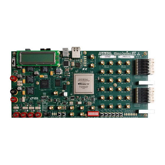
For information about setting up the Stratix IV GX transceiver signal integrity development board, and using the included software, refer to the Transceiver Signal Integrity Development Kit, Stratix IV GX Edition Getting Started User Guide. General Description The Stratix IV GX transceiver signal integrity development board provides a hardware platform for evaluating the performance and signal integrity features of the ®... - Page 6 ■ 100-MHz clock trigger output to SMA connector ■ Socketed clock trigger output to SMA connector ■ 156.25-MHz clock trigger output to SMA connector ■ Transceiver Signal Integrity Development Kit, November 2011 Altera Corporation Stratix IV GX Edition Reference Manual...
- Page 7 ■ On/Off slide power switch ■ On-Board power measurement circuitry ■ ■ Heat Sink and Fan 40-mm heat sink and 5-V DC fan combo ■ November 2011 Altera Corporation Transceiver Signal Integrity Development Kit, Stratix IV GX Edition Reference Manual...
-
Page 8: Development Board Block Diagram
Push Buttons Switches Displays 6 User 8 User 8 User DIP Rotary Push LEDs Switch Buttons 4 Menu Push Buttons 16 Char × 2 Line LCD Transceiver Signal Integrity Development Kit, November 2011 Altera Corporation Stratix IV GX Edition Reference Manual... -
Page 9: Handling The Board
The Stratix IV GX transceiver signal integrity board must be stored between –40º C and 100º C. The recommended operating temperature is between 0º C and 55º C. November 2011 Altera Corporation Transceiver Signal Integrity Development Kit, Stratix IV GX Edition Reference Manual... - Page 10 1–6 Chapter 1: Overview Handling the Board Transceiver Signal Integrity Development Kit, November 2011 Altera Corporation Stratix IV GX Edition Reference Manual...
-
Page 11: Chapter 2. Board Components
For information about powering up the board and installing the development kit software, refer to the Transceiver Signal Integrity Development Kit, Stratix IV GX Edition Getting Started User Guide. This chapter consists of the following sections: ■... -
Page 12: Board Overview
Table 2–1. Stratix IV GX Transceiver Signal Integrity Development Board Components (Part 1 of 4) Board Reference Type Description Featured Devices EP4SGX230KF40 Stratix IV GX device in a 1517-pin FBGA package. Configuration, Status, and Setup Elements Transceiver Signal Integrity Development Kit, November 2011 Altera Corporation Stratix IV GX Edition Reference Manual... - Page 13 JTAG for embedded JTAG for embedded USB-Blaster MAX II CPLD device programming. USB-Blaster MAX II CPLD Altera EPM1270256C3N, MAX II 256-pin CPLD for MAX II+Flash FPP MAX II CPLD configuration. Indicates an FPGA over-temperature condition exists and a fan should Fan LED be attached to the FPGA and running.
- Page 14 Flash memory 512-Mb flash memory. Components and Interfaces USB Type-B connector USB interface for embedded USB-Blaster. Altera EPM7064AETC44 MAX II CPLD device for embedded MAX II CPLD USB-Blaster circuitry. Ethernet RJ45 jack Halo HFJ11-1G02E RJ45 Ethernet jack with integrated magnetic.
- Page 15 (1) Information for the board reference whose components on the engineering silicon board differ from the production silicon board are listed in Table A–2 on page A–2. November 2011 Altera Corporation Transceiver Signal Integrity Development Kit, Stratix IV GX Edition Reference Manual...
-
Page 16: Featured Device: Stratix Iv Gx
Bank 2A Bank 5A EP4SGX230 Bank Bank GXBL2 GXBR2 Bank Bank GXBL1 GXBR1 Bank Bank GXBR0 GXBL0 *Number of Bank Transceiver Name Channel Number of I/Os Transceiver Signal Integrity Development Kit, November 2011 Altera Corporation Stratix IV GX Edition Reference Manual... - Page 17 Dedicated Configuration Pins CONFIG_DONE 2.5-V CMOS inout Dedicated Configuration Pins INIT_DONE 2.5-V CMOS output Dedicated Configuration Pins PGM[2:0] 2.5-V CMOS output Configuration Program Select Pins November 2011 Altera Corporation Transceiver Signal Integrity Development Kit, Stratix IV GX Edition Reference Manual...
- Page 18 Minimize Trace Length (2.5 in.) GXB0 Receive Channel Transceiver channel Minimize Trace Length (2.5 in.) GXB2 Long Transmit Channel Transceiver channel 33 in. Trace Length (8.5G) Transceiver Signal Integrity Development Kit, November 2011 Altera Corporation Stratix IV GX Edition Reference Manual...
-
Page 19: Configuration, Status, And Setup Elements
USB-Blaster. The USB-Blaster is implemented using a Type-B USB connector (CN1), a Future Technologies FT245BL USB PHY device (U16), and an Altera MAX7064 CPLD (U17). This allows configuration of the FPGA using a USB cable directly connected between the USB port on the board (CN1) and a USB port of a PC running the Quartus II software. -
Page 20: Fast Passive Parallel Download
PGMSEL (J62) selects between two Programmer Object Files (.pof)—factory .pof or user .pof files stored in the flash. The FPP controller uses the Altera Parallel Flash Loader (PFL) megafunction to configure the FPGA by reading data from the flash and converting it to FPP format. -
Page 21: Jtag Programming Header
(J28). This header provides another method for configuring the FPGA (U33) using an Altera USB-Blaster with the Quartus II Programmer running on a PC. The MAX II JTAG configuration jumper (J26) allows the MAX II CPLD device to be removed from the JTAG chain so that the FPGA is the only device on the JTAG chain. -
Page 22: Board Jumpers
When a jumper is installed on pins 1-2, FPP configuration loads the user POF image from flash. PGMSEL When a jumper is installed on pins 2-3, FPP configuration loads the factory POF image from flash. Transceiver Signal Integrity Development Kit, November 2011 Altera Corporation Stratix IV GX Edition Reference Manual... - Page 23 Table 2–9. Mini-DIP Switch Configuration (SW2) Clock Frequency Spread Spectrum % 25 MHz Center ±25 100 MHz Down –0.50 125 MHz Down –0.75 200 MHz No spread spectrum November 2011 Altera Corporation Transceiver Signal Integrity Development Kit, Stratix IV GX Edition Reference Manual...
-
Page 24: Clocks
EN JMP CLKBUF (J66) (Y4) (U23) Trigger SMA (J22) ICS85411 EN JMP 156.25 OSC CLKBUF (J67) Trigger (Y5) (U24) SMA (J23) CLKIN SMA (J19, J20) Transceiver Signal Integrity Development Kit, November 2011 Altera Corporation Stratix IV GX Edition Reference Manual... -
Page 25: General User Input/Output
Manufacturer Manufacturer Board Reference Manufacturer Description Part Number Website SW3–SW6, Push Buttons Panasonic Corporation EVQPAC07K www.panasonic.com SW8–SW15 D7–D15, Green LEDs Lumex Inc. SML-LX1206GC-TR www.lumex.com D17–D24 November 2011 Altera Corporation Transceiver Signal Integrity Development Kit, Stratix IV GX Edition Reference Manual... -
Page 26: Push Buttons
U33 pin G23 ENTR 10-kΩ pull-up push-buttons switches. These resistor to 2.5 V 2.5-V CMOS U33 pin G22 switches are not debounced. 2.5-V CMOS U33 pin H22 Transceiver Signal Integrity Development Kit, November 2011 Altera Corporation Stratix IV GX Edition Reference Manual... -
Page 27: User Leds
J24 pin 6 LCD_EN LCD DATA/CONTROL Signal U33 pin A18 J24 pin 4 LCD_D_Cn LCD Write Enable Strobe U33 pin A17 J24 pin 5 LCD_Wen November 2011 Altera Corporation Transceiver Signal Integrity Development Kit, Stratix IV GX Edition Reference Manual... -
Page 28: Dip Switch
2.5-V CMOS U33 pin M14 U32 pin F16 F_AD12 U39 pin A5 Flash Address bus bit 13 2.5-V CMOS U33 pin K15 U32 pin D16 F_AD13 Transceiver Signal Integrity Development Kit, November 2011 Altera Corporation Stratix IV GX Edition Reference Manual... - Page 29 Flash Write Protect 2.5-V CMOS U33 pin AT14 U32 pin T12 F_WPn U39 pin F7 Flash Busy 2.5-V CMOS U33 pin R14 U32 pin J14 F_BSYn November 2011 Altera Corporation Transceiver Signal Integrity Development Kit, Stratix IV GX Edition Reference Manual...
-
Page 30: Components And Interfaces
Figure 2–7. Temperature Measurement TEMPDIODE_P TEMPDIODE_N Stratix IV GX OVERTEMPn MAX1619 FPGA ALERTn (U15) (U33) SMBDATA SMBCLK Transceiver Signal Integrity Development Kit, November 2011 Altera Corporation Stratix IV GX Edition Reference Manual... - Page 31 Table 2–21. Temperature Sensor Component Reference Manufacturing Manufacturer Board Reference Description Manufacturer Part Number Website Dual temperature sensor with Maxim Integrated MAX1619MEE+T www.maxim-ic.com SMBus interface Products, Inc. November 2011 Altera Corporation Transceiver Signal Integrity Development Kit, Stratix IV GX Edition Reference Manual...
-
Page 32: Power Measurement
(1) The power rail measurements whose values on the engineering silicon board differ from the production silicon board are listed in Table A–3 on page A–2. Transceiver Signal Integrity Development Kit, November 2011 Altera Corporation Stratix IV GX Edition Reference Manual... -
Page 33: Ethernet Port
Board Manufacturing Manufacturer Description Manufacturer Reference Part Number Website Marvell 10/100/1000 Base-T Ethernet PHY 88E1111-B2-CAA1C000 www.marvell.com Semiconductor RJ45 with integrated magnetics Halo Electronics HFJ11-1G02ERL www.haloelectronics.com November 2011 Altera Corporation Transceiver Signal Integrity Development Kit, Stratix IV GX Edition Reference Manual... -
Page 34: Transceiver Channels
SMA connectors J38–J61. In the left GXB2 block, one transmit and one receive channel are sent to SMA connectors J31, J33, J35 and J37. Transceiver Signal Integrity Development Kit, November 2011 Altera Corporation Stratix IV GX Edition Reference Manual... -
Page 35: Power
U1 pin A10 — — RUN_SW Slide switch to OFF position to power U2 pin A10 off the board. U3 pin A10 November 2011 Altera Corporation Transceiver Signal Integrity Development Kit, Stratix IV GX Edition Reference Manual... -
Page 36: Power Distribution System
(U6, U9) Stratix IV GX Power 1.2 V VCC_1.2V LT3080-1 @ 1.1 A Ethernet (U25) Other Power LTC3025-1 1.8 V VCC_1.8V @ 0.5 A Flash (U38) Transceiver Signal Integrity Development Kit, November 2011 Altera Corporation Stratix IV GX Edition Reference Manual... -
Page 37: Banana Jacks And Fuses
VCC core Littelfuse Inc. 154 010.DR www.littlefuse.com Johnson Banana jack and fuse 111-0702-001 www.johnsoncomponents.com Components for supplying external power to VCCA Littelfuse Inc. 154 002 www.littlefuse.com November 2011 Altera Corporation Transceiver Signal Integrity Development Kit, Stratix IV GX Edition Reference Manual... - Page 38 (1) The banana jacks and fuses whose component reference on the engineering silicon board differ from the production silicon board are listed in Table A–4 on page A–3. Transceiver Signal Integrity Development Kit, November 2011 Altera Corporation Stratix IV GX Edition Reference Manual...
-
Page 39: Appendix A. Board Revision History
U39. The single-die package is smaller than the dual-die version. For more information about the flash change and its application, refer to the Transceiver Signal Integrity Development Kit, Stratix IV GX Edition Getting Started User Guide. Engineering Silicon Version Differences The engineering silicon version of the Stratix IV GX transceiver signal integrity development board is the initial release of the board. -
Page 40: Banana Jacks And Fuses
Failure to remove the associated fuses (F1–F7) or improperly setting the external supply voltages too high can result in damage to the board. Transceiver Signal Integrity Development Kit, November 2011 Altera Corporation Stratix IV GX Edition Reference Manual... - Page 41 VCCR Littelfuse Inc. 154 002 www.littlefuse.com Johnson Banana Jack and fuse 111-0702-001 www.johnsoncomponents.com Components for supplying external power to VCCT Littelfuse Inc. 154 002 www.littlefuse.com November 2011 Altera Corporation Transceiver Signal Integrity Development Kit, Stratix IV GX Edition Reference Manual...
- Page 42 A–4 Appendix A: Board Revision History Engineering Silicon Version Differences Transceiver Signal Integrity Development Kit, November 2011 Altera Corporation Stratix IV GX Edition Reference Manual...
-
Page 43: Additional Information
Nontechnical support (general) Email nacomp@altera.com (software licensing) Email authorization@altera.com Note to Table: (1) You can also contact your local Altera sales office or sales representative. November 2011 Altera Corporation Transceiver Signal Integrity Development Kit, Stratix IV GX Edition Reference Manual... -
Page 44: Typographic Conventions
The envelope links to the Email Subscription Management Center page of the Altera website, where you can sign up to receive update notifications for Altera documents. Transceiver Signal Integrity Development Kit, November 2011 Altera Corporation Stratix IV GX Edition Reference Manual...
Need help?
Do you have a question about the Stratix IV GX Edition and is the answer not in the manual?
Questions and answers