Table of Contents
Advertisement
Quick Links
8A3xxxx 72QFN
Evaluation Kit
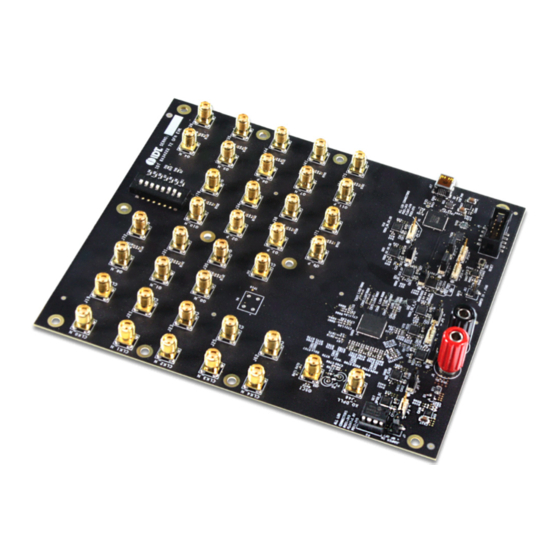
The 8A3xxxx 72QFN EVK allows customers to
evaluate Renesas' ClockMatrix devices (for example,
8A34005, 72QFN). This document discusses the
following:
▪ The board's design, its power supply, and jumper
settings
▪ The input and output connectors for normal
operation
▪ How to bring up the board using the Timing
Commander software GUI
▪ How to configure and program the board to
generate standard-compliant frequencies
Kit Contents
▪ 8A34xxx 72QFN Evaluation Board
▪ USB Type A cable
R31UH0015EU0101 Rev.1.01
Apr 26, 2022
PC Requirements
▪ Renesas
▪ ClockMatrix GUI
▪ USB 2.0 or USB 3.0 interface
▪ Windows XP SP3 or later
▪ Processor: Minimum 1GHz
▪ Memory: Minimum 512MB; recommended 1GB
▪ Available disk space: Minimum 600MB (1.5GB 64-
bit); recommended 1GB (2GB 64-bit)
▪ Network access during installation if the .NET
framework is not currently installed on the system
Figure 1. 8A3xxxx Evaluation Board
Evaluation Kit Manual
Timing Commander Software
© 2019-2022 Renesas Electronics
installed
Page 1
Advertisement
Table of Contents

Subscribe to Our Youtube Channel
Related Manuals for Renesas 8A3 72QFN Series


Summary of Contents for Renesas 8A3 72QFN Series
-
Page 1: Figure 1. 8A3Xxxx Evaluation Board
Evaluation Kit Manual 8A3xxxx 72QFN Evaluation Kit PC Requirements The 8A3xxxx 72QFN EVK allows customers to evaluate Renesas’ ClockMatrix devices (for example, ▪ Renesas Timing Commander Software installed 8A34005, 72QFN). This document discusses the ▪ ClockMatrix GUI following: ▪ USB 2.0 or USB 3.0 interface ▪... -
Page 2: Table Of Contents
8A3xxxx 72QFN Evaluation Kit Manual Contents Board Design ............... . 3 Board Power Supply . -
Page 3: Board Design
8A3xxxx 72QFN Evaluation Kit Manual Board Design The following diagram identifies the various components of the evaluation board: input and output SMA connectors, power supply jacks, and some jumper settings necessary for the board operations. Detailed descriptions are included below. Figure 2. -
Page 4: Board Power Supply
8A3xxxx 72QFN Evaluation Kit Manual ▪ SysDPLL Input (Optional) – An SMA connector, J46, is provided to supply a local OCXO/TCXO reference as an optional reference for System DPLL. ▪ Crystal: A crystal of various frequencies must be present for board operations. A 3225 footprint is provided for SMT crystals. -
Page 5: Gpio Switches, Leds, And Test Points
8A3xxxx 72QFN Evaluation Kit Manual GPIO Switches, LEDs, and Test Points An 8-bit dip switch sets the logic levels for seven GPIOs (GPIO0-5 and GPIO9). The GPIO levels for each setting and the corresponding LED state are listed in the following table (see picture and labels in Figure Table 1. -
Page 6: Working With Timing Commander™ For Programing / Configuration
8A3xxxx 72QFN Evaluation Kit Manual Working with Timing Commander™ for Programing / Configuration The following sections are best cross-referenced with the ClockMatrix GUI Step-by-Step User Guide that is available on the ClockMatrix Timing Solutions page and various ClockMatrix device product pages. Default Operation The board can operate off an EEPROM that has stored all information including firmware and a default configuration data. -
Page 7: Using Timing Commander To Control The Board
8A3xxxx 72QFN Evaluation Kit Manual Using Timing Commander to Control the Board Once the default operation is successful, complete the following steps to configure and program the ClockMatrix device per your specific application requirements using Timing Commander GUI tools: 1. Power up the board and set the main serial port in I2C mode by GPIO9 = “high”. Connect the board to the PC. 2. -
Page 8: Figure 7. Selecting 8A34001 Using Personality File V4.6
8A3xxxx 72QFN Evaluation Kit Manual Figure 7. Selecting 8A34001 using Personality File v4.6 4. The GUI window with the 8A34001 block diagram will open for configurations; or if “Open Settings File” is selected in Step 3 above, you will be prompted to browse and select an existing .tcs file and the personality file. When the configuration file is open, all configured values will be displayed as in Figure Figure 8. -
Page 9: Figure 9. Setting I2C For Connecting The Board With Gui
8A3xxxx 72QFN Evaluation Kit Manual 5. In order to connect the board with Timing Commander (PC), click the button (red circle) at the up-right corner of the GUI to set up the communication protocols (see Figure 8). After I2C and one-byte addressing are selected, click OK to close the window (seeFigure Figure 9. -
Page 10: Figure 11. Firmware Version Mismatch Warning Message
8A3xxxx 72QFN Evaluation Kit Manual Figure 11. Firmware Version Mismatch Warning Message 8. Once the connection is made, the firmware version can be read within the GUI. Click the “Firmware Utility” button to bring up the Firmware Utility window, as shown in Figure Figure 12. -
Page 11: Output Terminations And Rework To Take 1Pps Input
8A3xxxx 72QFN Evaluation Kit Manual 10. In the case where the firmware version mismatches each other, a firmware upgrade is necessary to update the device’s firmware. To update the device’s firmware, complete the Firmware Version Update steps in Appendix A: How to Upgrade the Firmware. -
Page 12: Schematics
8A3xxxx 72QFN Evaluation Kit Manual Schematics Schematic diagrams are located at the rear of the document. Ordering Information Part Number Description 8A34044-EVK 8A3xxxx 72QFN Evaluation Kit Revision History Revision Date Description ▪ Added updated Schematics. 1.01 Apr 26, 2022 ▪ Reformatted to the latest template. 1.00 Feb 14, 2019 Initial release... -
Page 13: Appendix A: How To Upgrade The Firmware
8A3xxxx 72QFN Evaluation Kit Manual Appendix A: How to Upgrade the Firmware Upload Firmware to the RAM 1. Connect to the EVB. 2. Power up the EVB with no EEPROM present. This ensures the firmware is 4.0.2.7017. 3. The GUI will indicate that the firmware on the chip does not match the GUI firmware. Press “Close”. 4. - Page 14 8A3xxxx 72QFN Evaluation Kit Manual 6. In the next dialog window, press “Yes” and wait approximately 3–4 minutes. 7. Once the FW updates, a dialog window will indicate a successful update. Click “Close”. 8. Press “Get Firmware Version” to verify that the RAM was updated correctly. When verified, click “Close”. R31UH0015EU0101 Rev.1.01 Page 14 Apr 26, 2022...
- Page 15 PROJECT NAME PROJECT NAME PROJECT NAME Fidus Systems Fidus Systems Fidus Systems Indira3 Indira3 Indira3 375 Terry Fox Drive, Ottawa, ON K2K 0J8 375 Terry Fox Drive, Ottawa, ON K2K 0J8 375 Terry Fox Drive, Ottawa, ON K2K 0J8 TITLE TITLE TITLE DESIGN...
- Page 16 VDDO_Q3 VDDO_Q2 VDDO_Q1 VDDO_Q0 VDDO_Q8 VDD_FOD_0 CLK_Q8_P CLK_Q8_N CLK_Q0_P CLK_Q0_N CLK_Q1_P CLK_Q1_N CLK_Q2_P CLK_Q2_N GPIO0 GPIO4 GPIO5 Maximum voltage on pin 7 = 1.8V U409 VDD_FOD VDDA_0 OSCO OSCO CLK_Q3_P OSCO OSCI VDDO_Q9 OSCI OSCI CLK_Q3_N SILKSCRN: VDD_FOD_0 VDDA_PDCP_XTAL VDDO_Q9 XO_DPLL VDDA_FB CLK_Q9_P...
- Page 17 Board 3V3 VDDD SILKSCRN: R9747 0.00 1206L350SLTHYR 3.3V Top VIN_1 VOUT_10 VIN_1 VOUT_10 2.5V Bot R599 R706 VIN_2 VOUT_9 C842 C963 VIN_2 VOUT_9 C864 C866 R703 10.0K 1.8V Float 1 9 - 0 2 - 1 4 R v R 26.7K 20.0K 111-0702-001...
- Page 18 VDDO_Q8_3_5 SILKSCRN: VDDO_Q2_4_11 3.3V Top SILKSCRN: VIN_1 VOUT_10 2.5V Bot 3.3V Top VIN_2 VOUT_9 VIN_1 VOUT_10 C971 C811 1.8V Float 10.0K 20.0K 2.5V Bot 0.1uF 22uF 10uF GND_8 VIN_2 VOUT_9 C983 C815 1.8V Float 10.0K 20.0K 12.0K 0.1uF 22uF SILKSCRN: 10uF CSET GND_8...
- Page 19 VCC_GPIO_DC 1V8_FTDI U403 3V3_FTDI VCCB VCCA R9771 5V0_USB R410 CLK_FTDI_PLL_SCL_OD VCORE ADBUS0 R411 FTDI_PLL_SDI_OD VCORE ADBUS1 R9770 FTDI_PLL_SDA_OD VCORE ADBUS2 R9760 ADBUS3 FTDI_PLL_nCS_OD VIN_8 VOUT_1 VCCIO ADBUS4 VCCIO ADBUS5 VIN_7 VOUT_2 VCCIO ADBUS6 VCCIO ADBUS7 VBUS R424 VREGOUT ACBUS0 GND_PAD USBD_P ENABLE VREGIN...
- Page 20 Note for Silkcreen: Place GPIO[x] lable close to each corresponding LED and Test point. VCC_GPIO_DC VCC_GPIO_DC VCC_GPIO_DC VCC_GPIO_DC R487 GPIO[0] R488 GPIO[1] R491 GPIO[2] R492 GPIO[3] LNJ347W83RA LNJ347W83RA LNJ347W83RA LNJ347W83RA GPIO0 GPIO0 GPIO0 GPIO1 GPIO2 GPIO3 GPIO1 GPIO1 GPIO2 GPIO2 GPIO3 GPIO3 GPIO4...
- Page 21 SILKSCRN: Place close to OSCI crystal Y3 R469 R470 R468 C759 1.0uF OSCI R471 R472 R9750 OSCO R9751 1 9 - 0 3 - 1 3 5-1814832-1 C765 12pF C766 12pF C996 0.1uF I2 Bus JP12~JP15 Default Jump Up 2 5 - 1 1 - 1 5 R117 CX3225GB50000P0HPQCC CLK_FTDI_PLL_SCL_OD...
- Page 22 TP19 SILKSCRN: R143 CLK_EXT_OSC CLK OSC PLACE NEAR OSCILLATOR 2 0 - 0 3 - 1 3 R K M6141LF R K 1 9 - 0 3 - 1 3 12.8MHZ MERC 9X7 HOT CMOS 3.3V OCXO 5-1814832-1 VDD_CLK0 VDD_CLK0 R912 R913 CLK4_P_SMA...
- Page 23 PLACE PARALLEL TERMINATIONS CLOSE TO U58 SILKSCRN: R731 R729 R730 SILKSCRN: SILKSCRN: Q0_P CLK_Q0_P CLK_Q4_P CLK_Q8_P Q4_P Q8_P R K 1 9 - 0 3 - 1 3 R K 1 9 - 0 3 - 1 3 R K 1 9 - 0 3 - 1 3 5-1814832-1 5-1814832-1 5-1814832-1...
- Page 24 VDDA VDDA_0 VDD_CLK0 VDD_CLK0_0 R875 R876 VDDA_1 R877 VDD_FOD R879 VDD_FOD_0 R882 VDD_FOD_2 VDDO_Q8_3_5 VDDO_Q8 VDDO_Q1_10_7 VDDO_Q1 R885 R886 R887 VDD_FOD_5 VDDO_Q3 VDDO_Q10 L100 R888 L103 R889 L104 VDDO_Q5 VDDO_Q7 R891 L105 R892 L106 VDDO_Q0_9_6 VDDO_Q0 VDDO_Q2_4_11 VDDO_Q2 R894 R895 VDDO_Q9 VDDO_Q4 R896...
- Page 25 Renesas' products are provided only subject to Renesas' Terms and Conditions of Sale or other applicable terms agreed to in writing. No use of any Renesas resources expands or otherwise alters any applicable warranties or warranty disclaimers for these products.
Need help?
Do you have a question about the 8A3 72QFN Series and is the answer not in the manual?
Questions and answers