Table of Contents
Advertisement
Quick Links
www.ti.com
User's Guide
TPS7H4010EVM User's Guide
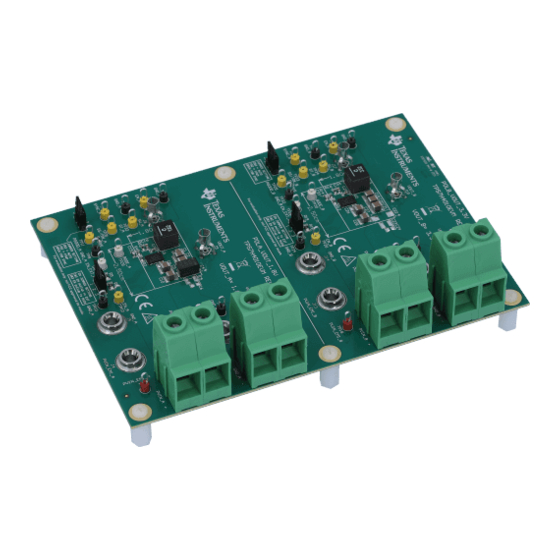
The TPS7H4010-SEP (Space Enhanced Plastic) evaluation module (EVM) with orderable part number
TPS7H4010EVM, is designed to help customers evaluate the performance of the TPS7H4010-SEP synchronous
step-down voltage converter. The EVM contains two independent buck converter circuits, each of which contains
the TPS7H4010-SEP which is in the 30-pin wettable flanks QFN (WQFN) package. The two circuits deliver very
accurate output voltages at 1.8 V and 3.3 V with up to 6 A current capacity with exceptional efficiency in a very
small solution size. The EVM provides multiple power connectors and test points, as well as mode setting and
enable input options, allowing for flexibility in testing.
1
Introduction.............................................................................................................................................................................3
1.1 TPS7H4010 Space Enhanced Plastic Evaluation Module.................................................................................................
Start...............................................................................................................................................................................6
3 Detailed Descriptions.............................................................................................................................................................
4
Schematic..............................................................................................................................................................................10
Layout.........................................................................................................................................................................12
6 Bill of Materials.....................................................................................................................................................................
Data....................................................................................................................................................19
Figure 1-1. TPS7H4010EVM.......................................................................................................................................................
Figure 4-1. TPS7H4010EVM PVIN=5 V, VOUT=1.8 V Schematic............................................................................................
Figure 4-2. TPS7H4010EVM PVIN=12 V, VOUT=3.3 V Schematic..........................................................................................
Figure 5-1. Top Layer and Silkscreen Layer..............................................................................................................................
Figure 5-2. Top Layer Routing...................................................................................................................................................
Figure 5-3. Mid-Layer 1 Ground Plane......................................................................................................................................
Figure 5-4. Mid-Layer 2 Routing................................................................................................................................................
Routing..............................................................................................................................................16
Figure 7-1. PVIN=5 V, VOUT=1.8 V, FSW=500 kHz: VOUT vs IOUT.......................................................................................
Figure 7-2. PVIN=5 V, VOUT=1.8 V, IOUT=6 A, FSW=500 kHz: Loop Response ...................................................................
Figure 7-3. PVIN=5 V, VOUT=1.8 V, FSW=500 kHz: Transient Response to current step from 2 A to 6 A at 1 A/us...............
Figure 7-4. PVIN=5 V, VOUT=1.8 V, FSW=500 kHz: Transient Response to current step from 6 A to 2 A at 1 A/us...............
Figure 7-5. PVIN=5 V, VOUT=1.8 V, IOUT=6 A, FSW=500 kHz: Output Voltage Ripple..........................................................
Figure 7-6. PVIN=5 V, VOUT=1.8 V, IOUT=6 A, FSW=500 kHz: Soft Start..............................................................................
Figure 7-8. PVIN=12 V, VOUT=3.3 V, FSW=500 kHz: VOUT vs IOUT.....................................................................................
Figure 7-9. PVIN=12 V, VOUT=3.3 V, IOUT=6 A, 3 A, 1 A, FSW=500 kHz: Loop Response ..................................................
Figure 7-12. PVIN=12 V, VOUT=3.3 V, IOUT= 6 A, FSW=500 kHz: Output Voltage Ripple.....................................................
SNVU744 - OCTOBER 2020
Submit Document Feedback
ABSTRACT
Table of Contents
Module.................................................................................................................................4
List of Figures
Schematic.....................................................................................................................................4
Marking..........................................................................................................................5
IOUT..........................................................................................................................22
Copyright © 2020 Texas Instruments Incorporated
Converter.........................................................................................3
kHz..............................................................................................19
kHz............................................................................................23
View)..................................................................4
Table of Contents
17
10
11
12
13
14
15
19
20
20
21
21
22
23
24
24
25
25
TPS7H4010EVM User's Guide
3
7
3
1
Advertisement
Table of Contents

Related Manuals for Texas Instruments TPS7H4010EVM


Summary of Contents for Texas Instruments TPS7H4010EVM
-
Page 1: Table Of Contents
The TPS7H4010-SEP (Space Enhanced Plastic) evaluation module (EVM) with orderable part number TPS7H4010EVM, is designed to help customers evaluate the performance of the TPS7H4010-SEP synchronous step-down voltage converter. The EVM contains two independent buck converter circuits, each of which contains the TPS7H4010-SEP which is in the 30-pin wettable flanks QFN (WQFN) package. - Page 2 Table 1-1. Device and Package Configurations...........................3 Table 1-2. Converter Circuit Variants............................Table 6-1. TPS7H4010EVM BOM............................. Trademarks All other trademarks are the property of their respective owners. TPS7H4010EVM User's Guide SNVU744 – OCTOBER 2020 Submit Document Feedback Copyright © 2020 Texas Instruments Incorporated...
-
Page 3: Introduction
Figure 1-1with orderable part number TPS7H4010EVM, is designed to help customers evaluate the performance of the TPS7H4010-SEP synchronous step-down voltage converter. The EVM contains two independent buck converter circuits, each of which contains the TPS7H4010-SEP which is in the 30-pin wettable flanks QFN (WQFN) package, as described Table 1-1. -
Page 4: Tps7H4010-Sep Evaluation Module
Figure 1-3. TPS7H4010-SEP Schematic Pin WQFN Package Top View) 1.3 TPS7H4010-SEP Evaluation Module The TPS7H4010-SEP evaluation module is orderable part number TPS7H4010EVM. The EVM contains two independent converter circuits targeting two common applications: • POLA: FSW=500 kHz, PVIN=5 V, VOUT=1.8 V, IOUT=0 A to 6 A •... -
Page 5: Figure 1-4. Tps7H4010-Sep Package
Introduction Figure 1-4. TPS7H4010-SEP Package Marking SNVU744 – OCTOBER 2020 TPS7H4010EVM User's Guide Submit Document Feedback Copyright © 2020 Texas Instruments Incorporated... -
Page 6: Quick Start
4. Turning on the PVIN power supply, the converter should provide a regulated V = 1.8 V across all current load conditions from 0 A to 6 A. TPS7H4010EVM User's Guide SNVU744 – OCTOBER 2020 Submit Document Feedback Copyright © 2020 Texas Instruments Incorporated... -
Page 7: Detailed Descriptions
Without control, excessive input voltage ripple can SNVU744 – OCTOBER 2020 TPS7H4010EVM User's Guide Submit Document Feedback Copyright © 2020 Texas Instruments Incorporated... - Page 8 DCM or continuous conduction mode (CCM) operation, the switching frequency is determined by the RT resistors (R6, R16) on the board, which is either 500 kHz. TPS7H4010EVM User's Guide SNVU744 – OCTOBER 2020 Submit Document Feedback Copyright © 2020 Texas Instruments Incorporated...
- Page 9 FPWM when synchronized to a clock. VCC_A (TP6) Test point to monitor the VCC pin VCC_B (TP20) This test point is to monitor the voltage at the VCC output. SNVU744 – OCTOBER 2020 TPS7H4010EVM User's Guide Submit Document Feedback Copyright © 2020 Texas Instruments Incorporated...
-
Page 10: Schematic
Schematic www.ti.com 4 Schematic The TPS7H4010EVM Schematic is shown in Figure 4-1 below. Figure 4-1. TPS7H4010EVM PVIN=5 V, VOUT=1.8 V Schematic TPS7H4010EVM User's Guide SNVU744 – OCTOBER 2020 Submit Document Feedback Copyright © 2020 Texas Instruments Incorporated... -
Page 11: Figure 4-2. Tps7H4010Evm Pvin=12 V, Vout=3.3 V Schematic
Schematic Figure 4-2. TPS7H4010EVM PVIN=12 V, VOUT=3.3 V Schematic SNVU744 – OCTOBER 2020 TPS7H4010EVM User's Guide Submit Document Feedback Copyright © 2020 Texas Instruments Incorporated... -
Page 12: Board Layout
Figure 5-1 through Figure 5-5 show the board layout for the TPS7H4010EVM. The EVM offers resistors, capacitors, and test points to configure the output voltage, precision enable pin, set frequency, and external clock synchronization. The 30-pin WQFN package offers an exposed thermal pad which must be soldered to the copper landing on the PCB for optimal thermal performance. -
Page 13: Figure 5-2. Top Layer Routing
Board Layout Figure 5-2. Top Layer Routing SNVU744 – OCTOBER 2020 TPS7H4010EVM User's Guide Submit Document Feedback Copyright © 2020 Texas Instruments Incorporated... -
Page 14: Figure 5-3. Mid-Layer 1 Ground Plane
Board Layout www.ti.com Figure 5-3. Mid-Layer 1 Ground Plane TPS7H4010EVM User's Guide SNVU744 – OCTOBER 2020 Submit Document Feedback Copyright © 2020 Texas Instruments Incorporated... -
Page 15: Figure 5-4. Mid-Layer 2 Routing
Board Layout Figure 5-4. Mid-Layer 2 Routing SNVU744 – OCTOBER 2020 TPS7H4010EVM User's Guide Submit Document Feedback Copyright © 2020 Texas Instruments Incorporated... -
Page 16: Figure 5-5. Bottom Layer Routing
Board Layout www.ti.com Figure 5-5. Bottom Layer Routing TPS7H4010EVM User's Guide SNVU744 – OCTOBER 2020 Submit Document Feedback Copyright © 2020 Texas Instruments Incorporated... -
Page 17: Bill Of Materials
Bill of Materials 6 Bill of Materials The bill of materials (BOM) of the TPS7H4010EVM is shown in Table 6-1 below. Table 6-1. TPS7H4010EVM BOM Designator Quantity Value Description Package Part Number Manufacturer Reference !PCB1 Printed Circuit Board LP044 C1, C8, C26 0.47 μF... - Page 18 Bill of Materials www.ti.com Table 6-1. TPS7H4010EVM BOM (continued) Designator Quantity Value Description Package Part Number Manufacturer Reference R6, R16 78.7 kΩ RES, 78.7 k, 1%, 0.1 W, 0603 0603 RC0603FR-0778K7L Yageo R8, R18 200 kΩ RES, 200 k, 1%, 0.125 W, AEC-Q200...
-
Page 19: Tps7H4010Evm Test Data
TPS7H4010EVM Test Data 7 TPS7H4010EVM Test Data 7.1 TPS7H4010EVM PVIN=5 V, VOUT=1.8 V, FSW=500 kHz All data presented is at ambient room temperature (~23C) with device in Auto Mode unless noted otherwise. Figure 7-1. PVIN=5 V, VOUT=1.8 V, FSW=500 kHz: VOUT vs IOUT... -
Page 20: Figure 7-2. Pvin=5 V, Vout=1.8 V, Iout=6 A, Fsw=500 Khz: Loop Response
Figure 7-2. PVIN=5 V, VOUT=1.8 V, IOUT=6 A, FSW=500 kHz: Loop Response Figure 7-3. PVIN=5 V, VOUT=1.8 V, FSW=500 kHz: Transient Response to current step from 2 A to 6 A at 1 A/us TPS7H4010EVM User's Guide SNVU744 – OCTOBER 2020 Submit Document Feedback Copyright © 2020 Texas Instruments Incorporated... -
Page 21: Figure 7-4. Pvin=5 V, Vout=1.8 V, Fsw=500 Khz: Transient Response To Current Step From 6 A To 2 A At 1 A/Us
Figure 7-4. PVIN=5 V, VOUT=1.8 V, FSW=500 kHz: Transient Response to current step from 6 A to 2 A at 1 A/us Figure 7-5. PVIN=5 V, VOUT=1.8 V, IOUT=6 A, FSW=500 kHz: Output Voltage Ripple SNVU744 – OCTOBER 2020 TPS7H4010EVM User's Guide Submit Document Feedback Copyright © 2020 Texas Instruments Incorporated... -
Page 22: Figure 7-6. Pvin=5 V, Vout=1.8 V, Iout=6 A, Fsw=500 Khz: Soft Start
TPS7H4010EVM Test Data www.ti.com Figure 7-6. PVIN=5 V, VOUT=1.8 V, IOUT=6 A, FSW=500 kHz: Soft Start Figure 7-7. FSW=500 kHz: Efficiency vs IOUT TPS7H4010EVM User's Guide SNVU744 – OCTOBER 2020 Submit Document Feedback Copyright © 2020 Texas Instruments Incorporated... -
Page 23: Tps7H4010Evm Pvin=12 V, Vout=3.3 V, Fsw=500 Khz
TPS7H4010EVM Test Data 7.2 TPS7H4010EVM PVIN=12 V, VOUT=3.3 V, FSW=500 kHz All data presented is at ambient room temperature (~23C) with device in Auto Mode unless noted otherwise. Figure 7-8. PVIN=12 V, VOUT=3.3 V, FSW=500 kHz: VOUT vs IOUT... -
Page 24: Figure 7-9. Pvin=12 V, Vout=3.3 V, Iout=6 A, 3 A, 1 A, Fsw=500 Khz: Loop Response
Figure 7-9. PVIN=12 V, VOUT=3.3 V, IOUT=6 A, 3 A, 1 A, FSW=500 kHz: Loop Response Figure 7-10. PVIN=12 V, VOUT=3.3 V, FSW=500 kHz: Transient Response to current step from 2 A to 6 A at 1 A/us TPS7H4010EVM User's Guide SNVU744 – OCTOBER 2020 Submit Document Feedback Copyright © 2020 Texas Instruments Incorporated... -
Page 25: Figure 7-11. Pvin=12 V, Vout=3.3 V, Fsw=500 Khz: Transient Response To Current Step From 6 A To 2 A At 1 A/Us
Figure 7-11. PVIN=12 V, VOUT=3.3 V, FSW=500 kHz: Transient Response to current step from 6 A to 2 A at 1 A/us Figure 7-12. PVIN=12 V, VOUT=3.3 V, IOUT= 6 A, FSW=500 kHz: Output Voltage Ripple SNVU744 – OCTOBER 2020 TPS7H4010EVM User's Guide Submit Document Feedback Copyright © 2020 Texas Instruments Incorporated... -
Page 26: Figure 7-13. Pvin=12 V, Vout=3.3 V, Iout= 6 A, Fsw=500 Khz: Soft Start
TPS7H4010EVM Test Data www.ti.com Figure 7-13. PVIN=12 V, VOUT=3.3 V, IOUT= 6 A, FSW=500 kHz: Soft Start Figure 7-14. FSW=500 kHz: Efficiency vs IOUT TPS7H4010EVM User's Guide SNVU744 – OCTOBER 2020 Submit Document Feedback Copyright © 2020 Texas Instruments Incorporated... - Page 27 STANDARD TERMS FOR EVALUATION MODULES Delivery: TI delivers TI evaluation boards, kits, or modules, including any accompanying demonstration software, components, and/or documentation which may be provided together or separately (collectively, an “EVM” or “EVMs”) to the User (“User”) in accordance with the terms set forth herein.
- Page 28 www.ti.com Regulatory Notices: 3.1 United States 3.1.1 Notice applicable to EVMs not FCC-Approved: FCC NOTICE: This kit is designed to allow product developers to evaluate electronic components, circuitry, or software associated with the kit to determine whether to incorporate such items in a finished product and software developers to write software applications for use with the end product.
- Page 29 www.ti.com Concernant les EVMs avec antennes détachables Conformément à la réglementation d'Industrie Canada, le présent émetteur radio peut fonctionner avec une antenne d'un type et d'un gain maximal (ou inférieur) approuvé pour l'émetteur par Industrie Canada. Dans le but de réduire les risques de brouillage radioélectrique à...
- Page 30 www.ti.com EVM Use Restrictions and Warnings: 4.1 EVMS ARE NOT FOR USE IN FUNCTIONAL SAFETY AND/OR SAFETY CRITICAL EVALUATIONS, INCLUDING BUT NOT LIMITED TO EVALUATIONS OF LIFE SUPPORT APPLICATIONS. 4.2 User must read and apply the user guide and other available documentation provided by TI regarding the EVM prior to handling or using the EVM, including without limitation any warning or restriction notices.
- Page 31 Notwithstanding the foregoing, any judgment may be enforced in any United States or foreign court, and TI may seek injunctive relief in any United States or foreign court. Mailing Address: Texas Instruments, Post Office Box 655303, Dallas, Texas 75265 Copyright © 2019, Texas Instruments Incorporated...
- Page 32 TI products. TI’s provision of these resources does not expand or otherwise alter TI’s applicable warranties or warranty disclaimers for TI products. Mailing Address: Texas Instruments, Post Office Box 655303, Dallas, Texas 75265 Copyright © 2020, Texas Instruments Incorporated...
Need help?
Do you have a question about the TPS7H4010EVM and is the answer not in the manual?
Questions and answers