Table of Contents
Advertisement
Quick Links
www.ti.com
User's Guide
TPS7H3302EVM (LP085)
This user's guide describes operational use of the TPS7H3302EVM evaluation module (EVM) as a reference
design for engineering demonstration and evaluation of the TPS7H3302-SEP, a 3-A sink and source DDR
termination LDO regulator. This user's guide provides details about the EVM, the configuration, schematics, and
bill of materials (BOM).
1
Introduction.............................................................................................................................................................................2
2 Description..............................................................................................................................................................................
Information............................................................................................................................................................3
Applications............................................................................................................................................................3
2.3 Features.............................................................................................................................................................................
Setup................................................................................................................................................................................4
3.1 Equipment..........................................................................................................................................................................
3.2 EVM Connectors and Test Points......................................................................................................................................
3.3 Testing Procedure..............................................................................................................................................................
Layout.........................................................................................................................................................................12
5
Schematic..............................................................................................................................................................................16
6 Bill of Materials.....................................................................................................................................................................
Documentation........................................................................................................................................................18
8 Revision History...................................................................................................................................................................
Figure 3-5. DDR3 Scope Plot of Response with 1.875 A Sinking Only with Isolated VDDQSNS.............................................
Figure 3-6. DDR3 Scope Plot of Response with 1.875 A Sourcing Only with Isolated VDDQSNS...........................................
Figure 3-7. DDR3 Scope Plot of Response With 1.875 A Sinking and Sourcing With Non-Isolated VDDQSNS......................
Figure 4-1. Top Overlay.............................................................................................................................................................
Figure 4-2. Top Solder...............................................................................................................................................................
Layer.................................................................................................................................................................13
Figure 4-4. Signal and Power Layer 1.......................................................................................................................................
Figure 4-5. Signal and Power Layer 2.......................................................................................................................................
Figure 4-6. Bottom Layer...........................................................................................................................................................
Solder..........................................................................................................................................................15
Schematic..................................................................................................................................................16
Table 3-1. Connectors and Test Points........................................................................................................................................
Materials..........................................................................................................................................................17
Trademarks
All trademarks are the property of their respective owners.
SLVUCK2A - JANUARY 2023 - REVISED APRIL 2023
Submit Document Feedback
ABSTRACT
Table of Contents
Summary.................................................................................................................................4
List of Figures
View)...........................................................................................................................2
mA...............................................................................................................................7
A......................................................................................................................................8
A......................................................................................................................................8
List of Tables
Summary..........................................................................................................................4
Points.........................................................................................................................6
Copyright © 2023 Texas Instruments Incorporated
Table of Contents
3
3
4
5
6
17
18
Isolated..........................10
10
11
11
12
12
13
14
14
5
TPS7H3302EVM (LP085)
1
Advertisement
Table of Contents

Related Manuals for Texas Instruments TPS7H3302EVM LP085


Summary of Contents for Texas Instruments TPS7H3302EVM LP085
-
Page 1: Table Of Contents
Table 3-2. I/O Voltage Measurement Test Points.........................6 Table 6-1. Bill of Materials................................17 Trademarks All trademarks are the property of their respective owners. SLVUCK2A – JANUARY 2023 – REVISED APRIL 2023 TPS7H3302EVM (LP085) Submit Document Feedback Copyright © 2023 Texas Instruments Incorporated... -
Page 2: Introduction
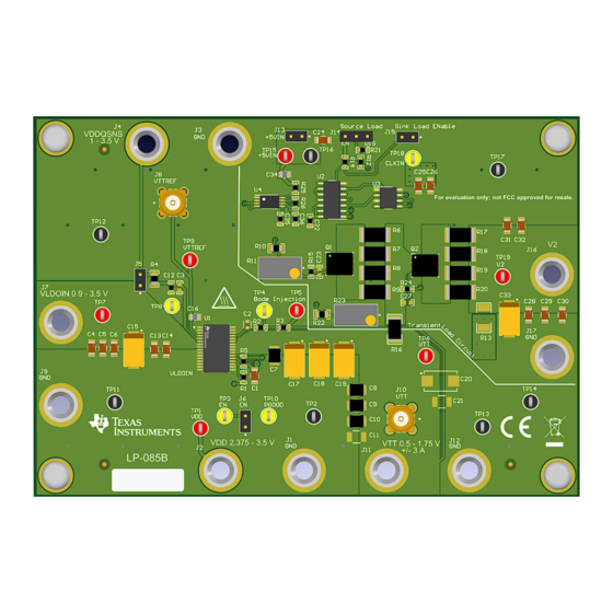
The TPS7H3302EVM-SEP (LP085) evaluation board is designed to evaluate the performance and characteristics of TI's radiation tolerant DDR/DDR2/DDR3/DDR3L/DDR4 termination regulator, the TPS7H3302- SEP. Figure 1-1. TPS7H3302EVM Board (Top View) TPS7H3302EVM (LP085) SLVUCK2A – JANUARY 2023 – REVISED APRIL 2023 Submit Document Feedback Copyright © 2023 Texas Instruments Incorporated... -
Page 3: Description
Convenient test points for probing PGOOD, CLK_IN, and loop response testing • Optional placeholders for VDDQSNS to VLDOIN filter when not using independent VDDQSNS source SLVUCK2A – JANUARY 2023 – REVISED APRIL 2023 TPS7H3302EVM (LP085) Submit Document Feedback Copyright © 2023 Texas Instruments Incorporated... -
Page 4: Performance Specification Summary
3.1.2 Load #1 Electronic load capable of testing desired DC sink or source load current (up to 3 A). TPS7H3302EVM (LP085) SLVUCK2A – JANUARY 2023 – REVISED APRIL 2023 Submit Document Feedback Copyright © 2023 Texas Instruments Incorporated... -
Page 5: Evm Connectors And Test Points
TP16 Test point Ground (GND) TP17 Test point Ground (GND) TP18 Test point Clock TP19 Test point for voltage source V2 SLVUCK2A – JANUARY 2023 – REVISED APRIL 2023 TPS7H3302EVM (LP085) Submit Document Feedback Copyright © 2023 Texas Instruments Incorporated... -
Page 6: Testing Procedure
1.2 V ≤ VDDQSNS ≤ 3.5 V J4 or (Pin2 J5)(+) TP12(–) ½ VDDQSNS TP6(+) TP13(–) VTTREF ½ VDDQSNS TP9(+) TP11(–) TPS7H3302EVM (LP085) SLVUCK2A – JANUARY 2023 – REVISED APRIL 2023 Submit Document Feedback Copyright © 2023 Texas Instruments Incorporated... -
Page 7: Figure 3-1. Ddr3 Bode Plot Iload = 500 Ma
VTT load 500 mA Gain Phase -100 -120 -140 -160 -180 -100 -200 100k Frequency Figure 3-1. DDR3 Bode Plot Iload = 500 mA SLVUCK2A – JANUARY 2023 – REVISED APRIL 2023 TPS7H3302EVM (LP085) Submit Document Feedback Copyright © 2023 Texas Instruments Incorporated... -
Page 8: Figure 3-2. Ddr3 Bode Plot Iload
VLDOIN and VDDQSNS. Adding an RC filter between VLDOIN and VDDQSNS results in some loss of dynamic tracking of VTT and VTTREF to VDDQSNS. TPS7H3302EVM (LP085) SLVUCK2A – JANUARY 2023 – REVISED APRIL 2023 Submit Document Feedback Copyright © 2023 Texas Instruments Incorporated... - Page 9 R4, and C3. Note the large fluctuation on VTTREF due to VLDOIN and hence VDDQSNS transients. SLVUCK2A – JANUARY 2023 – REVISED APRIL 2023 TPS7H3302EVM (LP085) Submit Document Feedback Copyright © 2023 Texas Instruments Incorporated...
-
Page 10: Figure 3-4. Ddr3 Scope Plot Response With Both Sinking And Sourcing Enabled And Vddqsns Isolated
Figure 3-4. DDR3 Scope Plot Response With Both Sinking and Sourcing Enabled and VDDQSNS Isolated. Figure 3-5. DDR3 Scope Plot of Response with 1.875 A Sinking Only with Isolated VDDQSNS TPS7H3302EVM (LP085) SLVUCK2A – JANUARY 2023 – REVISED APRIL 2023 Submit Document Feedback Copyright © 2023 Texas Instruments Incorporated... -
Page 11: Figure 3-6. Ddr3 Scope Plot Of Response With 1.875 A Sourcing Only With Isolated Vddqsns
Figure 3-6. DDR3 Scope Plot of Response with 1.875 A Sourcing Only with Isolated VDDQSNS Figure 3-7. DDR3 Scope Plot of Response With 1.875 A Sinking and Sourcing With Non-Isolated VDDQSNS SLVUCK2A – JANUARY 2023 – REVISED APRIL 2023 TPS7H3302EVM (LP085) Submit Document Feedback Copyright © 2023 Texas Instruments Incorporated... -
Page 12: Board Layout
Board Layout www.ti.com 4 Board Layout Figure 4-1. Top Overlay Figure 4-2. Top Solder TPS7H3302EVM (LP085) SLVUCK2A – JANUARY 2023 – REVISED APRIL 2023 Submit Document Feedback Copyright © 2023 Texas Instruments Incorporated... -
Page 13: Figure 4-3. Top Layer
Board Layout Figure 4-3. Top Layer Figure 4-4. Signal and Power Layer 1 SLVUCK2A – JANUARY 2023 – REVISED APRIL 2023 TPS7H3302EVM (LP085) Submit Document Feedback Copyright © 2023 Texas Instruments Incorporated... -
Page 14: Figure 4-5. Signal And Power Layer 2
Board Layout www.ti.com Figure 4-5. Signal and Power Layer 2 Figure 4-6. Bottom Layer TPS7H3302EVM (LP085) SLVUCK2A – JANUARY 2023 – REVISED APRIL 2023 Submit Document Feedback Copyright © 2023 Texas Instruments Incorporated... -
Page 15: Figure 4-7. Bottom Solder
Board Layout Figure 4-7. Bottom Solder SLVUCK2A – JANUARY 2023 – REVISED APRIL 2023 TPS7H3302EVM (LP085) Submit Document Feedback Copyright © 2023 Texas Instruments Incorporated... -
Page 16: Schematic
0.9-3.5V 10µF 10µF 10µF 10µF 10µF RESET DISCH 47uF 7.5k 2.2µF THRES CONT 100nF 100nF TRIG NE555PWR Figure 5-1. LP085B Schematic TPS7H3302EVM (LP085) SLVUCK2A – JANUARY 2023 – REVISED APRIL 2023 Submit Document Feedback Copyright © 2023 Texas Instruments Incorporated... -
Page 17: Bill Of Materials
ESR03EZPJ102 Rohm 0603 Resistor, 7.5 kΩ, 5%, 0.1 W, 0603 RC0603JR-077K5L Yageo SH-J1,SH-J2,SH-J3 Shunt, 100 mil, gold plated, black SNT-100-BK-G Samtec SLVUCK2A – JANUARY 2023 – REVISED APRIL 2023 TPS7H3302EVM (LP085) Submit Document Feedback Copyright © 2023 Texas Instruments Incorporated... -
Page 18: Related Documentation
Deleted notes pertaining to revision A board......................7 • Changed board plots to LP085B........................• Changed schematic to LP085B........................• Change Bill of Materials to LP085B........................17 TPS7H3302EVM (LP085) SLVUCK2A – JANUARY 2023 – REVISED APRIL 2023 Submit Document Feedback Copyright © 2023 Texas Instruments Incorporated... - Page 19 STANDARD TERMS FOR EVALUATION MODULES Delivery: TI delivers TI evaluation boards, kits, or modules, including any accompanying demonstration software, components, and/or documentation which may be provided together or separately (collectively, an “EVM” or “EVMs”) to the User (“User”) in accordance with the terms set forth herein.
- Page 20 www.ti.com Regulatory Notices: 3.1 United States 3.1.1 Notice applicable to EVMs not FCC-Approved: FCC NOTICE: This kit is designed to allow product developers to evaluate electronic components, circuitry, or software associated with the kit to determine whether to incorporate such items in a finished product and software developers to write software applications for use with the end product.
- Page 21 www.ti.com Concernant les EVMs avec antennes détachables Conformément à la réglementation d'Industrie Canada, le présent émetteur radio peut fonctionner avec une antenne d'un type et d'un gain maximal (ou inférieur) approuvé pour l'émetteur par Industrie Canada. Dans le but de réduire les risques de brouillage radioélectrique à...
- Page 22 www.ti.com EVM Use Restrictions and Warnings: 4.1 EVMS ARE NOT FOR USE IN FUNCTIONAL SAFETY AND/OR SAFETY CRITICAL EVALUATIONS, INCLUDING BUT NOT LIMITED TO EVALUATIONS OF LIFE SUPPORT APPLICATIONS. 4.2 User must read and apply the user guide and other available documentation provided by TI regarding the EVM prior to handling or using the EVM, including without limitation any warning or restriction notices.
- Page 23 Notwithstanding the foregoing, any judgment may be enforced in any United States or foreign court, and TI may seek injunctive relief in any United States or foreign court. Mailing Address: Texas Instruments, Post Office Box 655303, Dallas, Texas 75265 Copyright © 2023, Texas Instruments Incorporated...
- Page 24 TI products. TI’s provision of these resources does not expand or otherwise alter TI’s applicable warranties or warranty disclaimers for TI products. TI objects to and rejects any additional or different terms you may have proposed. IMPORTANT NOTICE Mailing Address: Texas Instruments, Post Office Box 655303, Dallas, Texas 75265 Copyright © 2023, Texas Instruments Incorporated...
Need help?
Do you have a question about the TPS7H3302EVM LP085 and is the answer not in the manual?
Questions and answers