Table of Contents
Advertisement
Quick Links
www.ti.com
User's Guide
TPS7H1101SPEVM User's Guide
1
Introduction.............................................................................................................................................................................2
Documentation......................................................................................................................................................2
2 Description..............................................................................................................................................................................
Setup................................................................................................................................................................................3
3.1 Equipment..........................................................................................................................................................................
3.2 Bench Test Setup Conditions.............................................................................................................................................
Procedure..........................................................................................................................................................4
4 Board Layout.........................................................................................................................................................................
4.1 EVM Layout Flexibility......................................................................................................................................................
Materials...........................................................................................................................................17
History.......................................................................................................................................................................20
Figure 3-3. IOUT (A) vs IPCL (A) across CSR range..................................................................................................................
Figure 3-4. VCS (V) vs IOUT (A).................................................................................................................................................
............................................................................................................................................................7
Figure 3-7. Load Transient Response: Step Load 0.1 A to 1.6 mA.............................................................................................
Figure 3-8. Expanded View Overshoot........................................................................................................................................
Figure 3-9. Expanded View Undershoot......................................................................................................................................
Figure 3-10. Current Sharing LDO_1 and LDO_2.......................................................................................................................
Figure 3-12. Turn-Off.................................................................................................................................................................
Figure 4-2. Component Placement (Bottom
Figure 4-3. PCB Layout (Top Layer)..........................................................................................................................................
Figure 4-4. Board Layout - Second Layer (Mid Layer 1)...........................................................................................................
Figure 4-5. Board Layout - Third Layer (Mid Layer 2)...............................................................................................................
Trademarks
All trademarks are the property of their respective owners.
SLVU944B - OCTOBER 2015 - REVISED OCTOBER 2020
Submit Document Feedback
Table of Contents
List of Figures
Placement............................................................................................................3
(uA)...............................................................................................................................................5
(A)...................................................................................................................................................6
Pin......................................................................................................................10
Side)...........................................................................................................................11
Side).....................................................................................................................12
Layer)...........................................................................................................16
Schematic...............................................................................................................................17
Copyright © 2020 Texas Instruments Incorporated
Table of Contents
TPS7H1101SPEVM User's Guide
2
3
3
11
11
5
6
7
8
8
9
10
13
14
15
1
Advertisement
Table of Contents

Related Manuals for Texas Instruments TPS7H1101SPEVM


Summary of Contents for Texas Instruments TPS7H1101SPEVM
-
Page 1: Table Of Contents
Figure 4-6. Board Layout - Fourth Layer (Bottom Layer)......................16 Figure 5-1. TPS7H1101SPEVM Schematic..........................17 Trademarks All trademarks are the property of their respective owners. SLVU944B – OCTOBER 2015 – REVISED OCTOBER 2020 TPS7H1101SPEVM User’s Guide Submit Document Feedback Copyright © 2020 Texas Instruments Incorporated... -
Page 2: Introduction
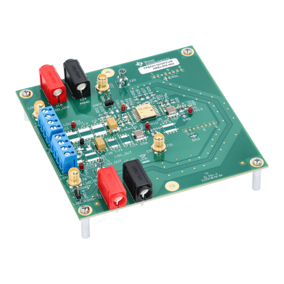
This user’s guide includes setup instructions, a schematic diagram, a bill of materials (BOM), and PCB layout drawings for the EVM. 1.1 Related Documentation TPS7H1101A (SLVSDW6) Data Sheet 2 Description The TPS7H1101SPEVM helps designers evaluate the operation and performance of the TPS7H1101A-SP ultra LDO regulator. Table 2-1. Summary of Performance Test Conditions Output Current Range = 1.5 V to 7 V... -
Page 3: Test Setup
An Tektronix Oscilloscope, for example, DPO 7104CCurrent Probe Tektronix TCP202 or equivalent. 3.2 Bench Test Setup Conditions 3.2.1 Headers Description and Jumper Placement Figure 3-1. Headers Description and Jumper Placement SLVU944B – OCTOBER 2015 – REVISED OCTOBER 2020 TPS7H1101SPEVM User’s Guide Submit Document Feedback Copyright © 2020 Texas Instruments Incorporated... -
Page 4: Power-Up Procedure
A resistor value R30 connected from PCL pin to GND determines the output current limit set point based on Equation TPS7H1101SPEVM User’s Guide SLVU944B – OCTOBER 2015 – REVISED OCTOBER 2020 Submit Document Feedback Copyright © 2020 Texas Instruments Incorporated... -
Page 5: Figure 3-2. Iout (A) Vs Ipcl (Ua)
Vin = 2.28 V and R23 = 3.65 kΩ. A resistor connected from current sense (CS) pin to V indicates voltage proportional to the output current. SLVU944B – OCTOBER 2015 – REVISED OCTOBER 2020 TPS7H1101SPEVM User’s Guide Submit Document Feedback Copyright © 2020 Texas Instruments Incorporated... -
Page 6: Figure 3-4. Vcs (V) Vs Iout (A)
) is the difference between the input voltage and output voltage needed to maintain regulation. V vs I is highlighted in Figure 3-6. TPS7H1101SPEVM User’s Guide SLVU944B – OCTOBER 2015 – REVISED OCTOBER 2020 Submit Document Feedback Copyright © 2020 Texas Instruments Incorporated... -
Page 7: Figure 3-6. Vdo Vs Iout
Channel 2: Step load in current Channel 3: Input voltage Figure 3-7. Load Transient Response: Step Load 0.1 A to 1.6 mA SLVU944B – OCTOBER 2015 – REVISED OCTOBER 2020 TPS7H1101SPEVM User’s Guide Submit Document Feedback Copyright © 2020 Texas Instruments Incorporated... -
Page 8: Figure 3-8. Expanded View Overshoot
Test Setup www.ti.com Figure 3-8. Expanded View Overshoot Figure 3-9. Expanded View Undershoot TPS7H1101SPEVM User’s Guide SLVU944B – OCTOBER 2015 – REVISED OCTOBER 2020 Submit Document Feedback Copyright © 2020 Texas Instruments Incorporated... -
Page 9: Figure 3-10. Current Sharing Ldo_1 And Ldo_2
2N7002 MOSFET as shown in Figure 3-11. A high signal at the gate of Q100 will discharge the SS pin and disable the device. SLVU944B – OCTOBER 2015 – REVISED OCTOBER 2020 TPS7H1101SPEVM User’s Guide Submit Document Feedback Copyright © 2020 Texas Instruments Incorporated... -
Page 10: Figure 3-11. Disabling The Ldo Via Soft-Start Pin
Test Setup www.ti.com Figure 3-11. Disabling the LDO via Soft-Start Pin 3.3.11 Turn-Off Figure 3-12. Turn-Off TPS7H1101SPEVM User’s Guide SLVU944B – OCTOBER 2015 – REVISED OCTOBER 2020 Submit Document Feedback Copyright © 2020 Texas Instruments Incorporated... -
Page 11: Board Layout
Additionally, placeholder is provided thus one can add esr in series with the output capacitor (R47 in series with C39) thus making it easier to evaluate performance with increased capacitor esr. Figure 4-1. Component Placement (Top Side) SLVU944B – OCTOBER 2015 – REVISED OCTOBER 2020 TPS7H1101SPEVM User’s Guide Submit Document Feedback Copyright © 2020 Texas Instruments Incorporated... -
Page 12: Figure 4-2. Component Placement
Board Layout www.ti.com Figure 4-2. Component Placement (Bottom Side) TPS7H1101SPEVM User’s Guide SLVU944B – OCTOBER 2015 – REVISED OCTOBER 2020 Submit Document Feedback Copyright © 2020 Texas Instruments Incorporated... -
Page 13: Figure 4-3. Pcb Layout (Top Layer)
Board Layout Figure 4-3. PCB Layout (Top Layer) SLVU944B – OCTOBER 2015 – REVISED OCTOBER 2020 TPS7H1101SPEVM User’s Guide Submit Document Feedback Copyright © 2020 Texas Instruments Incorporated... -
Page 14: Figure 4-4. Board Layout - Second Layer (Mid Layer 1)
Board Layout www.ti.com Figure 4-4. Board Layout - Second Layer (Mid Layer 1) TPS7H1101SPEVM User’s Guide SLVU944B – OCTOBER 2015 – REVISED OCTOBER 2020 Submit Document Feedback Copyright © 2020 Texas Instruments Incorporated... -
Page 15: Figure 4-5. Board Layout - Third Layer (Mid Layer 2)
Board Layout Figure 4-5. Board Layout - Third Layer (Mid Layer 2) SLVU944B – OCTOBER 2015 – REVISED OCTOBER 2020 TPS7H1101SPEVM User’s Guide Submit Document Feedback Copyright © 2020 Texas Instruments Incorporated... -
Page 16: Figure 4-6. Board Layout - Fourth Layer
Board Layout www.ti.com Figure 4-6. Board Layout - Fourth Layer (Bottom Layer) TPS7H1101SPEVM User’s Guide SLVU944B – OCTOBER 2015 – REVISED OCTOBER 2020 Submit Document Feedback Copyright © 2020 Texas Instruments Incorporated... -
Page 17: Schematic And Bill Of Materials
101_ 14 PS7H1 VOUT 101_7 101_ 16 TPS7H1101_9 TPS7H1101_1 TPS7H1101_ 1 6 AGND AGND AGND HDR_1X8_100MIL HDR_1X8_100MIL Figure 5-1. TPS7H1101SPEVM Schematic SLVU944B – OCTOBER 2015 – REVISED OCTOBER 2020 TPS7H1101SPEVM User’s Guide Submit Document Feedback Copyright © 2020 Texas Instruments Incorporated... - Page 18 Schematic and Bill of Materials www.ti.com Table 5-1. TPS7H1101SPEVM Bill of Materials ITEM NO. DESIGNATOR VALUE FOOTPRINT MANUFACTURER PART NO. DESCRIPTION 220uF 7260-38 Kemet T543X227M016ATE035 CAP TANT 220UF 16V 20% 2917 C32,C61 10nF 0805 Kemet C0805C103K3RACTU CAP CER 10000PF 25V 10% X7R 0805...
- Page 19 Schematic and Bill of Materials Table 5-1. TPS7H1101SPEVM Bill of Materials (continued) ITEM NO. DESIGNATOR VALUE FOOTPRINT MANUFACTURER PART NO. DESCRIPTION Keystone 2029K-ND Standoffs Pencom 4-40X1/4PH-PN-MS-SS Screws for standoffs HREL008 HREL008 Label on the EVM under TI logo =...
-
Page 20: Revision History
Changes from Revision * (September 2013) to Revision A (October 2015) Page • Corrected the y-axis scale in the image......................5 TPS7H1101SPEVM User’s Guide SLVU944B – OCTOBER 2015 – REVISED OCTOBER 2020 Submit Document Feedback Copyright © 2020 Texas Instruments Incorporated... - Page 21 STANDARD TERMS FOR EVALUATION MODULES Delivery: TI delivers TI evaluation boards, kits, or modules, including any accompanying demonstration software, components, and/or documentation which may be provided together or separately (collectively, an “EVM” or “EVMs”) to the User (“User”) in accordance with the terms set forth herein.
- Page 22 www.ti.com Regulatory Notices: 3.1 United States 3.1.1 Notice applicable to EVMs not FCC-Approved: FCC NOTICE: This kit is designed to allow product developers to evaluate electronic components, circuitry, or software associated with the kit to determine whether to incorporate such items in a finished product and software developers to write software applications for use with the end product.
- Page 23 www.ti.com Concernant les EVMs avec antennes détachables Conformément à la réglementation d'Industrie Canada, le présent émetteur radio peut fonctionner avec une antenne d'un type et d'un gain maximal (ou inférieur) approuvé pour l'émetteur par Industrie Canada. Dans le but de réduire les risques de brouillage radioélectrique à...
- Page 24 www.ti.com EVM Use Restrictions and Warnings: 4.1 EVMS ARE NOT FOR USE IN FUNCTIONAL SAFETY AND/OR SAFETY CRITICAL EVALUATIONS, INCLUDING BUT NOT LIMITED TO EVALUATIONS OF LIFE SUPPORT APPLICATIONS. 4.2 User must read and apply the user guide and other available documentation provided by TI regarding the EVM prior to handling or using the EVM, including without limitation any warning or restriction notices.
- Page 25 Notwithstanding the foregoing, any judgment may be enforced in any United States or foreign court, and TI may seek injunctive relief in any United States or foreign court. Mailing Address: Texas Instruments, Post Office Box 655303, Dallas, Texas 75265 Copyright © 2019, Texas Instruments Incorporated...
- Page 26 TI products. TI’s provision of these resources does not expand or otherwise alter TI’s applicable warranties or warranty disclaimers for TI products. Mailing Address: Texas Instruments, Post Office Box 655303, Dallas, Texas 75265 Copyright © 2020, Texas Instruments Incorporated...
Need help?
Do you have a question about the TPS7H1101SPEVM and is the answer not in the manual?
Questions and answers