Table of Contents
Advertisement
Quick Links
www.ti.com
User's Guide
TPS7H4011-SP (TPS7H4011EVM-CVAL) Evaluation Module
This user's guide describes the characteristics, operation, and use of the TPS7H4011EVM-CVAL board. This
evaluation module (EVM) is optimized for 4.5V to 14V input voltage range and 12A maximum output current. The
feedback divider and compensation network can be modified for other application conditions according to the
TPS7H4011-SP data
sheet.
1 Description..............................................................................................................................................................................
2
Features...................................................................................................................................................................................2
3 Evaluation Module Overview.................................................................................................................................................
3.1 Introduction........................................................................................................................................................................
Contents........................................................................................................................................................................3
3.3
Specification.......................................................................................................................................................................3
3.4 Device Information.............................................................................................................................................................
4 Hardware.................................................................................................................................................................................
4.1
Setup..................................................................................................................................................................................5
Descriptions......................................................................................................................................................5
4.3 Best Practices....................................................................................................................................................................
5 Implementation Results.........................................................................................................................................................
5.1 Default Configuration Results............................................................................................................................................
5.2 Soft Startup........................................................................................................................................................................
5.3 Voltage Ripple on VOUT....................................................................................................................................................
Step.........................................................................................................................................................................10
5.5 Frequency Response.......................................................................................................................................................
6 Hardware Design Files.........................................................................................................................................................
6.1
Schematics.......................................................................................................................................................................12
6.2 PCB Layouts....................................................................................................................................................................
6.3 Bill of Materials (BOM).....................................................................................................................................................
Information.......................................................................................................................................................22
Documentation........................................................................................................................................................23
Trademarks
All trademarks are the property of their respective owners.
SLVUCK1 - APRIL 2024
Submit Document Feedback
ABSTRACT
Table of Contents
Copyright © 2024 Texas Instruments Incorporated
TPS7H4011-SP (TPS7H4011EVM-CVAL) Evaluation Module
Table of Contents
2
3
3
4
5
7
8
8
8
9
11
12
13
18
1
Advertisement
Table of Contents

Related Manuals for Texas Instruments TPS7H4011-SP


Summary of Contents for Texas Instruments TPS7H4011-SP
-
Page 1: Table Of Contents
6.2 PCB Layouts..................................6.3 Bill of Materials (BOM)..............................7 Compliance Information...............................22 8 Related Documentation................................23 Trademarks All trademarks are the property of their respective owners. SLVUCK1 – APRIL 2024 TPS7H4011-SP (TPS7H4011EVM-CVAL) Evaluation Module Submit Document Feedback Copyright © 2024 Texas Instruments Incorporated... -
Page 2: Description
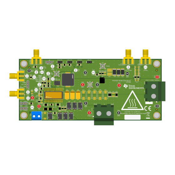
Selectable current limit, switching frequency, and slope compensation • High-current transient test circuit • 0.6V ±0.67% voltage reference over line, temperature, and radiation Figure 2-1. EVM Board TPS7H4011-SP (TPS7H4011EVM-CVAL) Evaluation Module SLVUCK1 – APRIL 2024 Submit Document Feedback Copyright © 2024 Texas Instruments Incorporated... -
Page 3: Evaluation Module Overview
SS_TR FB_BOT FAULT VSNS- AVDD PWRGD LDOCAP PWRGD ILIM COMP ILIM_TOP COMP SYNCM REFCAP ILIM_BOT COMP SYNC1 PGND SYNC2 Figure 3-1. Simplified Schematic SLVUCK1 – APRIL 2024 TPS7H4011-SP (TPS7H4011EVM-CVAL) Evaluation Module Submit Document Feedback Copyright © 2024 Texas Instruments Incorporated... -
Page 4: Device Information
The wide voltage range of the TPS7H4011-SP enables it to be used as a point of load regulator to convert directly from a 12V rail. Additionally, various features are included such as differential remote sensing, selectable current limit, a flexible fault input pin, and configurable compensation. -
Page 5: Hardware
333mΩ load resistance created by 3, 1Ω chip resistors connected in parallel. While the CSD16408Q5 power MOSFET is capable of conducting the full 12A output current of the TPS7H4011-SP, the chip resistors are each rated for only 2W. When utilizing the transient circuit on the TPS7H4011EVM-CVAL, the signal sent to the MOSFET gate through TP30 (TRANS) can be modulated to keep the average power through the load resistors below the 2W rating. - Page 6 VOUTremote+ TP30 TRANS TP31 Vremote- VOUT Compact probe tip connector TRANS ILIM_19A RSC_SEL FSW_SEL ILIM_14A Jumper for mode selection SYNCM ILIM_9A SYNC2 ILIM6A TPS7H4011-SP (TPS7H4011EVM-CVAL) Evaluation Module SLVUCK1 – APRIL 2024 Submit Document Feedback Copyright © 2024 Texas Instruments Incorporated...
-
Page 7: Best Practices
Some components can reach high temperatures > 55°C when the board is powered on. Do not touch the board at any point during operation or immediately after operating, as high temperatures can be present. SLVUCK1 – APRIL 2024 TPS7H4011-SP (TPS7H4011EVM-CVAL) Evaluation Module Submit Document Feedback Copyright © 2024 Texas Instruments Incorporated... -
Page 8: Implementation Results
5-1. Table 5-1. Test Settings SPECIFICATION VALUE VOUT 3.3V 500kHz ILIM 18.3A 511kΩ 5.2 Soft Startup Figure 5-1. Soft Startup Into 275mΩ Load TPS7H4011-SP (TPS7H4011EVM-CVAL) Evaluation Module SLVUCK1 – APRIL 2024 Submit Document Feedback Copyright © 2024 Texas Instruments Incorporated... -
Page 9: Voltage Ripple On Vout
To avoid coupled noise from the switch node, output voltage ripple was measured across C24 using a "tip-and-barrel" method with a coil wire ground. Figure 5-2. Output Voltage Ripple SLVUCK1 – APRIL 2024 TPS7H4011-SP (TPS7H4011EVM-CVAL) Evaluation Module Submit Document Feedback Copyright © 2024 Texas Instruments Incorporated... -
Page 10: Load Step
Figure 5-3. Transiant Response to Load Step 100mA to 12A at 8A/µs Figure 5-4. Transiant Response to Load Step 12A to 100mA at 8A/µs TPS7H4011-SP (TPS7H4011EVM-CVAL) Evaluation Module SLVUCK1 – APRIL 2024 Submit Document Feedback Copyright © 2024 Texas Instruments Incorporated... -
Page 11: Frequency Response
Implementation Results 5.5 Frequency Response Figure 5-5. Frequency Response IOUT = 6A SLVUCK1 – APRIL 2024 TPS7H4011-SP (TPS7H4011EVM-CVAL) Evaluation Module Submit Document Feedback Copyright © 2024 Texas Instruments Incorporated... -
Page 12: Hardware Design Files
TRANS AUX_5V 2.23k 49.9 TP31 FB/NC Vremote- Vremote- 10µF VSNS- 1.00 1.00 1.00 0.01 100nF 3.3µF Thermal_pad TPS7B8450QWDRBRQ1 Figure 6-1. Default EVM Schematic TPS7H4011-SP (TPS7H4011EVM-CVAL) Evaluation Module SLVUCK1 – APRIL 2024 Submit Document Feedback Copyright © 2024 Texas Instruments Incorporated... -
Page 13: Pcb Layouts
Hardware Design Files 6.2 PCB Layouts Figure 6-2. Top Overlay Figure 6-3. Top Solder Mask Figure 6-4. Layer 1 (Top) SLVUCK1 – APRIL 2024 TPS7H4011-SP (TPS7H4011EVM-CVAL) Evaluation Module Submit Document Feedback Copyright © 2024 Texas Instruments Incorporated... - Page 14 Hardware Design Files www.ti.com Figure 6-5. Layer 2 Figure 6-6. Layer 3 Figure 6-7. Layer 4 TPS7H4011-SP (TPS7H4011EVM-CVAL) Evaluation Module SLVUCK1 – APRIL 2024 Submit Document Feedback Copyright © 2024 Texas Instruments Incorporated...
- Page 15 Hardware Design Files Figure 6-8. Layer 5 Figure 6-9. Layer 6 Figure 6-10. Layer 7 SLVUCK1 – APRIL 2024 TPS7H4011-SP (TPS7H4011EVM-CVAL) Evaluation Module Submit Document Feedback Copyright © 2024 Texas Instruments Incorporated...
- Page 16 Hardware Design Files www.ti.com Figure 6-11. Layer 8 (Bottom) Figure 6-12. Bottom Solder Mask Figure 6-13. Bottom Overlay TPS7H4011-SP (TPS7H4011EVM-CVAL) Evaluation Module SLVUCK1 – APRIL 2024 Submit Document Feedback Copyright © 2024 Texas Instruments Incorporated...
- Page 17 Hardware Design Files Figure 6-14. Drill Drawing SLVUCK1 – APRIL 2024 TPS7H4011-SP (TPS7H4011EVM-CVAL) Evaluation Module Submit Document Feedback Copyright © 2024 Texas Instruments Incorporated...
-
Page 18: Bill Of Materials (Bom)
Screw NY PMS 440 0025 PH B&F Fastener Supply Philips panhead H5, H6, H7, H8 Standoff, Hex, 0.5"L #4-40 Nylon Standoff 1902C Keystone TPS7H4011-SP (TPS7H4011EVM-CVAL) Evaluation Module SLVUCK1 – APRIL 2024 Submit Document Feedback Copyright © 2024 Texas Instruments Incorporated... - Page 19 RES, 49.9 k, 1%, 0.125 W, AEC-Q200 Grade 0, R9, R12, R18 49.9k 0805 ERJ-6ENF4992V Panasonic 0805 43.2k RES, 43.2 k, 0.1%, 0.125 W, 0805 0805 RT0805BRD0743K2L Yageo America SLVUCK1 – APRIL 2024 TPS7H4011-SP (TPS7H4011EVM-CVAL) Evaluation Module Submit Document Feedback Copyright © 2024 Texas Instruments Incorporated...
- Page 20 Cap Tant Polymer 100uF 25VDC D CASE 20% 100µF (7.3 X 4.3 X 2.8mm) SMD 7343-31 0.04 Ohm 2917 T521D107M025ATE040 KEMET 105C T/R TPS7H4011-SP (TPS7H4011EVM-CVAL) Evaluation Module SLVUCK1 – APRIL 2024 Submit Document Feedback Copyright © 2024 Texas Instruments Incorporated...
- Page 21 RES, 2.21 k, 0.1%, 0.125 W, 0805 0805 RT0805BRD072K21L Yageo America 10 mOhms ±1% 10W Chip Resistor 2817 (7142 0.01 2817 GMR320HJBFA10L0 ROHM Metric) Current Sense Metal Element SLVUCK1 – APRIL 2024 TPS7H4011-SP (TPS7H4011EVM-CVAL) Evaluation Module Submit Document Feedback Copyright © 2024 Texas Instruments Incorporated...
-
Page 22: Compliance Information
Compliance Information www.ti.com 7 Compliance Information • Texas Instruments, TPS7H4011EVM-CVAL EU RoHS Declaration of Conformity (DoC) TPS7H4011-SP (TPS7H4011EVM-CVAL) Evaluation Module SLVUCK1 – APRIL 2024 Submit Document Feedback Copyright © 2024 Texas Instruments Incorporated... -
Page 23: Related Documentation
Related Documentation 8 Related Documentation • Texas Instruments, TPS7H4011-SP and TPS7H4011-SEP 4.5V to 14V Input 12A Radiation Hardened Synchronous Buck Converter data sheet • Texas Instruments, N-Channel NexFET™ Power MOSFET (CSD16408Q5) data sheet SLVUCK1 – APRIL 2024 TPS7H4011-SP (TPS7H4011EVM-CVAL) Evaluation Module Submit Document Feedback Copyright ©... - Page 24 STANDARD TERMS FOR EVALUATION MODULES Delivery: TI delivers TI evaluation boards, kits, or modules, including any accompanying demonstration software, components, and/or documentation which may be provided together or separately (collectively, an “EVM” or “EVMs”) to the User (“User”) in accordance with the terms set forth herein.
- Page 25 www.ti.com Regulatory Notices: 3.1 United States 3.1.1 Notice applicable to EVMs not FCC-Approved: FCC NOTICE: This kit is designed to allow product developers to evaluate electronic components, circuitry, or software associated with the kit to determine whether to incorporate such items in a finished product and software developers to write software applications for use with the end product.
- Page 26 www.ti.com Concernant les EVMs avec antennes détachables Conformément à la réglementation d'Industrie Canada, le présent émetteur radio peut fonctionner avec une antenne d'un type et d'un gain maximal (ou inférieur) approuvé pour l'émetteur par Industrie Canada. Dans le but de réduire les risques de brouillage radioélectrique à...
- Page 27 www.ti.com EVM Use Restrictions and Warnings: 4.1 EVMS ARE NOT FOR USE IN FUNCTIONAL SAFETY AND/OR SAFETY CRITICAL EVALUATIONS, INCLUDING BUT NOT LIMITED TO EVALUATIONS OF LIFE SUPPORT APPLICATIONS. 4.2 User must read and apply the user guide and other available documentation provided by TI regarding the EVM prior to handling or using the EVM, including without limitation any warning or restriction notices.
- Page 28 Notwithstanding the foregoing, any judgment may be enforced in any United States or foreign court, and TI may seek injunctive relief in any United States or foreign court. Mailing Address: Texas Instruments, Post Office Box 655303, Dallas, Texas 75265 Copyright © 2023, Texas Instruments Incorporated...
- Page 29 TI products. TI’s provision of these resources does not expand or otherwise alter TI’s applicable warranties or warranty disclaimers for TI products. TI objects to and rejects any additional or different terms you may have proposed. IMPORTANT NOTICE Mailing Address: Texas Instruments, Post Office Box 655303, Dallas, Texas 75265 Copyright © 2024, Texas Instruments Incorporated...
Need help?
Do you have a question about the TPS7H4011-SP and is the answer not in the manual?
Questions and answers