Table of Contents
Advertisement
Quick Links
Advertisement
Table of Contents

Related Manuals for JHCTech KMDA-2701


Summary of Contents for JHCTech KMDA-2701
- Page 1 User’s Manual User’s Manual KMDA-2701 Ver.A1.0 Date:15, October, 2018...
- Page 2 User’s Manual Version Note Ver. Note Date Writer A1.0 first publish 20180815 Tracy Liu...
- Page 3 Microsoft Windows and MS-DOS are registered trademarks of Microsoft Corp. RTL is a trademark of Realtek Semi-Conductor Co., Ltd. All other product names or trademarks are properties of their respective owners. For more information on this and other JHC products, please visit our websites at: http://www.jhctech.com.cn...
- Page 4 User’s Manual Product Warranty (2 years) JHC warrants to you, the original purchaser, that each of its products will be free from defects in materials and workmanship for two years from the date of purchase. This warranty does not apply to any products which have been repaired or altered by persons other than repair personnel authorized by JHC, or which have been subject to misuse, abuse, accident or improper installation.
- Page 5 Technical Support and Assistance Step 1. Visit the JHC web site at www.jhctech.com.cn where you can find the latest information about the product. Step 2. Contact your distributor, sales representative, or JHC’s customer service center for technical support if you need additional assistance.
-
Page 6: Table Of Contents
User’s Manual CONTENTS GENERAL INFORMATION ............................ 1 1.1 I ..............................2 NTRODUCTION 1.2 F ................................ 2 EATURES 1.3 S ............................... 2 PECIFICATIONS 1.3.1 General ..............................2 1.3.2 Display ..............................3 1.3.3 Ethernet ..............................3 1.3.4 Audio ............................... 3 1.3.5 Power Consumption ..........................3 1.4 E ......................... - Page 7 User’s Manual 3.4 B ..............................51 3.5 S ............................... 52 ECURITY 3.6 S & E ............................53 3.7 U BIOS ............................53 PDATING THE DRIVER INSTALLATION ............................. 55 4.1 A DVD-ROM/CD-ROM ....................56 BOUT THE OFTWARE 4.2 A 8/10 ...................... 56 INSTALLING UNDER INDOWS 4.3 M...
-
Page 8: General Information
User’s Manual General Information... -
Page 9: Introduction
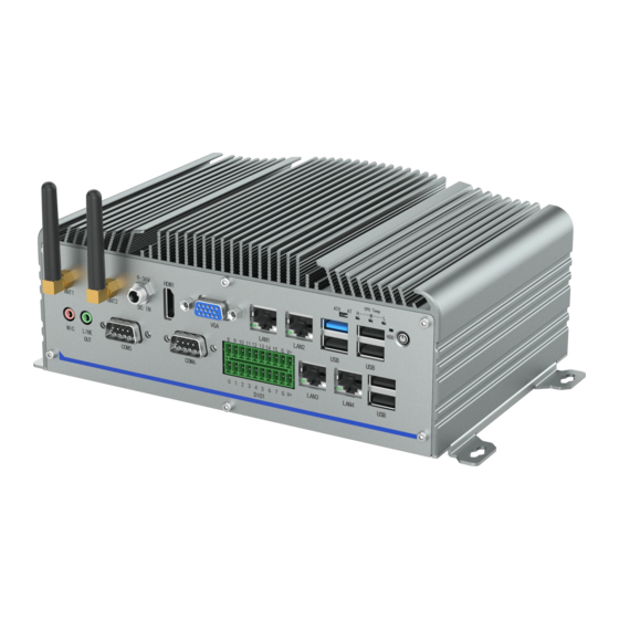
6*USB2.0 ports (1 inside), 1*Audio line out, 1*MIC, 6*COM ports, 24-bit DIO ports, 2*Mini PCIe sockets one with PCIe and USB signal, one with SATA and USB signal; The KMDA-2701 supports 1*3.5 inches SATA HDD driver bay, 1* mSATA for storage, DC 9-36V wide power input. Besides, operating temperature showing in LEDs, economic and reliable, it will be fit for security and manufacture application. -
Page 10: Display
User’s Manual Serial Ports: 2* RS-232 DB9 male, 4* RS-232/422/485, DB9 male USB: 1*USB 3.0 Type A port, 5*USB2.0 Type A ports(Front),1* USB 2.0 Type A port (inside) Expansion Interface: 1* Mini PCIe with PCIeX1\ USB2.0 signal, 1*micro Sim slot for 4G LTE/WiFi/BT etc 1* Mini PCIe with SATA3\ USB2.0 signal, used to be mSATA Storage: 1* mSATA (Full size), dual AHCI... -
Page 11: Mechanical Specifications
User’s Manual -10 ~ 55° C (Fanless with HDD, Airflow) Relative humidity: 10~90% @ 40° C (non-condensing) Storage temperature: -40 ~ 85° C (-40 ~ 185° F) Vibration loading during operation: With SSD: 5 Grms, random, 5 ~ 500 Hz With HDD:1 Grms, random, 5 ~ 500 Hz Shock during operation: With SSD: 50g, peak acceleration (11 ms duration) - Page 12 User’s Manual Main board (rear) Figure 1.1 Sub-board(ECB 154) Figure 1.2...
- Page 13 User’s Manual KMDA-2701 Dimensions: Uint: mm Figure 1.3...
-
Page 14: Hardware Installation
User’s Manual Hardware Installation... -
Page 15: Introduction
2.2 Jumpers and connectors The KMDA-2701 Fanless Embedded Box Computer consists of an JHC SBC (Single Board Computer) board and an JHC sub-board that is housed in an aluminum plate chassis. Warning: Do not remove any mechanical parts until you have verified that no power is flowing within the Embedded Box Computer. -
Page 16: Setting Jumpers
2.2.1 Setting Jumpers You can configure your KMDA-2701 to match the needs of your application by setting the jumpers. A jumper is the simplest kind of electrical switch. It consists of two metal pins and a small metal clip (often protected by a plastic cover) that slides over the pins to connect them. -
Page 17: Jumper Location
2.3 Jumper Location The KMDA-2701 Embedded Box Computer has a number of jumpers inside the chassis that allows you to configure your system to suit your application. The table below lists the functions of the various jumpers. -
Page 18: Clear Cmos Data
User’s Manual 2.3.1 Clear CMOS Data Figure 2.6 If you encounter the followings a) CMOS data becomes corrupted. b) You forget the supervisor or user password. you can reconfigure the system with the default values stored in the ROM BIOS. To load the default values stored in the ROM BIOS, please follow the steps below. -
Page 19: Lvds Power Supply 12V/5V/3.3V Mode Select
User’s Manual 2.3.2 LVDS Power supply 12V/5V/3.3V Mode Select Figure 2.7 J_PANEL is used to select the power supplied of LVDS panel. 2.3.3 COM5/COM6 RS232/RS485/RS422 Mode Select Figure 2.8 NOTE:JP1 is for COM5; JP3 is for COM6. -
Page 20: Com5/Com6 Matching Resistor Select Jumper
User’s Manual 2.3.4 COM5/COM6 Matching resistor Select Jumper Figure 2.9 NOTE:JP2 is for COM5; JP4 is for COM6. 2.3.5 COM5/COM6 RI/5V/12V Power supply Select Figure 2.10 NOTE: Pin 12 and 34 are for COM5; Pin 56 and 78 are for COM6. -
Page 21: I/O、Button And Led Indication
User’s Manual 2.4 I/O、Button and LED indication Front view Figure 2.11 Rear view Figure 2.12... -
Page 22: Ethernet Connector (Lan)
2.4.2 Power Input Connector (DC-IN) The KMDA-2701 uses a power socket that supports up to 60W of power and is a low-power solution. Using a 12V adapter to input voltage and a DC power supply to the outlet. If the voltage used is greater than the recommended voltage, the system will not boot or even damage the motherboard. -
Page 23: Usb Connector
The USB2.0 pin definition is as follows: Figure 2.15 USB2.0 connector Table 2.2: USB2.0 Connector Signal USB_VCC USB_D- USB_D+ USB_GND The KMDA-2701 provides one USB3.0 port by type A connector. Please refer to Table 2.3 for their pin assignments. Figure 2.16: USB3.0 Connector... -
Page 24: Hdmi
GND_DRAIN StdA_SSTX- StdA_SSTX+ Shell Shield 2.4.4 HDMI The KMDA-2701 provides a high-resolution HDMI display port, it supports the most resolution up to 1920*1080@60Hz. The Pin assignments are as follows: Figure 2.17 HDMI Connector Table 2.4: HDMI Pin Assignments Signal Signal... -
Page 25: Vga Connector
GREEN BLUE Note: NC represents —No Connection The KMDA-2701 provides a high-resolution VGA interface via D-sub 15-pin connector to support a VGA CRT monitor, it supports the most resolution up to 1920*1080@60Hz. 2.4.6 COM1/2 Connector The KMDA-2701 provides 2 serial ports of COM1/2 by 2*D-sub 9-pin connectors. COM1/2 can be configured as RS232、RS422 or RS485 by BIOS setup. -
Page 26: Com3/4 Connector
User’s Manual Note: NC represents —No Connection 2.4.7 COM3/4 Connector Figure 2.20 COM3/4 Connector COM3/4 are only for RS232. The Pin assignments are as follows: Table 2.7: COM3/4 Serial Port Pin Assignments Signal Signal 2.4.8 COM5/6 Connector Figure 2.21 COM5/6 Connector... -
Page 27: Dio Connector
DATA- DATA+ RI/5V/12V 2.4.9 DIO Connector The KMDA-2701 provides a 24-bit DIO by a 2*10Pin 16-bit DIO terminal connector and a 2*5Pin 8-bit DIO terminal connector in rear. The Pin assignments are as follows: Figure 2.22 8-bit DIO Connector Table 2.9: 8-bit DIO Pin Assignments... -
Page 28: Sata2.0 Port Connector
DIO2_7 DIO2_15 2.4.10 SATA2.0 Port connector The KMDA-2701 provides a serial ATA 2.0 port with data transfer rate up to 3Gb/s. The Serial ATA connector is used to connect Serial ATA devices. The Pin assignments are as follows: Figure 2.24... -
Page 29: Sata Power Connector
Pin-1 of PWOUT to avoid possible damage to the board and hard disk driver! 2.4.12 Line-Out and Mic Connector The KMDA-2701 provides a Line-Out connector and a Mic connector for audio output and input. 2.4.13 I-port Connector There are optional 1*USB2.0 or Mini PCIe module I/O ports(such as CAN Bus, Gig LAN etc.). -
Page 30: At/Atx Sw
2.4.15 AT/ATX SW The KMDA-2701 provides a AT/ATX SW, which users can set Power-on mode by it. When you dial it at AT, it means power on by AC Power; When you dial it at ATX, it means power on by Power button. - Page 31 User’s Manual Step 9: Close the bottom cover back to the chassis. install the front panel and screw 2 screws on the front/rear panel. Step 10: Screw 5 screws and 6 serial copper columns on the front panel. Lock the spring pad and nut of the DC-IN on the front panel.
- Page 32 User’s Manual Figure 2.29 Figure 2.30 Figure 2.31...
- Page 33 User’s Manual Figure 2.32 Figure 2.33 Figure 2.34...
- Page 34 User’s Manual Figure 2.35 Figure 2.36 Figure 2.37...
-
Page 35: Installing Mini Pcie Module
User’s Manual 2.5.2 Installing Mini PCIe Module Step 1: Unscrew 4 screws on the bottom cover, remove the bottom bracket. Unscrew 2 screws on the front/rear panel. Rotate the bottom assembly 180° , separate the SATA cable which connected the HDD/SSD with the mother board. - Page 36 User’s Manual Figure 2.40 Figure 2.41 Figure 2.42...
- Page 37 User’s Manual Figure 2.43 Step 2: Hold the Mini PCIe module with its notch aligned with the Mini PCIe socket of the board and insert it at a 30 degrees angle into the socket as shown in the picture. Figure 2.44 Step 3: Screw one screw to the holder as shown in the picture.
- Page 38 User’s Manual Step 4: Install the sub-card on the mainboard, Screw 7 screws on the sub-card. Install the front panel. Screw 5 screws and 6 serial coppers on the front panel, lock the nut and spring pad of the DC-IN. Install the rear panel.
- Page 39 User’s Manual Figure 2.48 Figure 2.49 Figure 2.50...
-
Page 40: Installing Msata
User’s Manual Figure 2.51 2.5.3 Installing MSATA Step 1: The step here is the same as above chapter “ 2.5.2 Installing Mini PCIe Module -Step 1”, For details, please refer to the above chapter “ 2.5.2 Installing Mini PCIe Module -Step 1”... - Page 41 User’s Manual Step 3. Screw one screw to the holder as shown in the picture. Figure 2.53 Step 4. The step here is the same as above chapter “ 2.5.2 Installing Mini PCIe Module -Step 4”, For details, please refer to the above chapter “ 2.5.2 Installing Mini PCIe Module -Step 4”...
-
Page 42: Bios Setup
User’s Manual BIOS Setup... -
Page 43: Ami Bios Description
User’s Manual 3.1 AMI BIOS Description When booting, the BIOS will self-diagnose the hardware on the motherboard, set hardware timing parameters, etc., and finally hand over the system control to the operating system. BIOS is the communication bridge between hardware and software. How to correctly set the BIOS parameters is crucial for the system to work stably and whether the system works at its best. -
Page 44: Main Menu
User’s Manual For the purpose of better product maintenance, the manufacture reserves the right to change the BIOS items presented in this manual. The BIOS setup screens shown in this chapter are for reference only and may differ from the actual BIOS. Please visit the manufacture’s website for updated manual. 3.2.2 Main Menu When you enter the BIOS Setup program, the main menu appears, giving you an overview of the basic system information. -
Page 45: Advanced Menu
User’s Manual 3.2.3 Advanced Menu This page sets up more advanced information about your system. Handle this page with caution. Any changes can affect the operation of your computer. Figure 3.2 ▶ ACPI Settings The item in the menu shows the highest ACPI sleep state when the system enters suspend. Figure 3.3... - Page 46 User’s Manual ACPI Sleep State Suspend Disabled: Shut down system sleep S3:Suspend to RAM This item allows user to enter the ACPI S3 (Suspend toRAM) Sleep State (default). Press <Esc> to return to the Advanced Menu page. ▶ IT8786 Supper IO Configuration The item in the menu shows the information of RTC wake settings.
- Page 47 User’s Manual Figure 3.5 Serial Port This item is used to set the serial interface to be turned on or off. The setting value is [Enabled] [Disabled] Device Setting (Read Only) This item displays the interrupt and address of the serial port. Change Setting Set port interrupt and address of the serial port.
- Page 48 User’s Manual Figure 3.7 Serial Port 5-10Configuration Serial Port 5-10 Configuration is the same as above ▶ H/W Monitor PC Health Status This item is used for hardware security detection. The BIOS will display the current CPU and system temperature. Figure 3.8...
- Page 49 User’s Manual ▶ S5 RTC Wake Settings Figure 3.9 Wake system from S5 This item is used to set whether to power on regularly. The setting value is [Enabled] [Disabled]. If you select [Enabled], set the hour, minute, and second in the pop-up options. ▶...
- Page 50 User’s Manual ▶ CPU Configuration This item in the menu shows the information of the CPU. Figure 3.11 Socket 0 CPU Information This item contains detailed information about the CPU, including the CPU manufacturer, model, frequency, L1 cache size, and L2 cache size. CPU Speed This item shows the processor speed.
- Page 51 User’s Manual malicious attacks based on buffer overflow viruses. In addition, the execution of the prohibition bit requires Windows XP SP2, Windows Server 2003 SP1 and other OS to work properly. The implementation principle is that the processor divides several areas in memory, some areas can execute application code, while others do not allow.
- Page 52 User’s Manual ▶ SATA Configuration This item in the menu shows the mode of serial ATA configuration options. Figure 3.13 Serial-ATA(SATA) This item allows you to enable or disable serial-ATA. SATA Speed Support This item shows the speed of support SATA. Press <Esc>...
- Page 53 User’s Manual ▶ CSM Configuration Figure 3.14 CSM Support Compatibility Support Module, which is a compatibility support module, is a special module of UEFI and provides compatibility support for systems that do not support UEFI. GateA20 Active This item indicates whether to disable GA20 through the BIOS server or keep the activation status all the time.
- Page 54 User’s Manual Other PCI devices This item is used to set the EFI PCI device OpROM boot or the traditional PCI device OpROM boot ▶ USB Configuration Use this item to show the information of USB configuration. Figure 3.15 Legacy USB Support This item is used to set the USB interface support.
-
Page 55: Chipset Menu
User’s Manual USB Transfer time-out This item Sets the timeout period for control, batch, and interrupt transmission. The default is 20 seconds. Device reset time-out This item sets boot command timeout of the large capacity USB disk. The default is 20 seconds. Device Power-up Delay This item sets the maximum delay time that the USB device reports to the primary controller. - Page 56 User’s Manual ▶ North Bridge Scroll to this item and press <Enter> and view the following screen: Figure 3.17 Integrated Graphics Device This item indicates whether integrated graphics is enabled. Primary Display This item shows the main output display device when the system starts up. DVMT pre-AIIocated This item sets the memory size pre-assigned to the motherboard integrated graphics in DVMT mode.
- Page 57 User’s Manual Primary IGFX Boot Display This item sets IGFX main display device on POST stage, not affected by external graphics card, options are LVDS, CRT, HDMI. It defaults by VBIOS. Secondary IGFX Boot Display This item sets IGFX second display device on POST stage. LCD Panel Type This item sets resolution of the motherboard LVDS screen.
-
Page 58: Boot Menu
User’s Manual 3.2.5 Boot Menu This page enables you to set the keyboard Num-Lock state and devices boot sequence. Figure 3.20 Setup Prompt Timeout This item sets the wait time for the Setup shortcut. If you do not press the Setup shortcut within the set time, it will continue to boot. -
Page 59: Security Menu
User’s Manual Hard Drive BBS Priorities Figure 3.21 This item sets the hard disk that can be used as the boot device. If there are multiple hard disks, you should select the priority of these hard disks in the item. The highest priority hard disk will be displayed in Boot Option #1. -
Page 60: Save & Exit Menu
User’s Manual 3.2.7 Save & Exit Menu This page enables you to exit system setup after saving or without saving the changes. Figure 3.23 Save Changes and Exit This item enables you to save the changes that you have made and exit. Discard Changes and Exit This item enables you to discard any changes that you have made and exit. - Page 61 User’s Manual Fpt64.efi is a FLASH IC read/write program that loads BIOS data on the motherboard and needs to be operated in a shell environment. Please boot the system into the shell environment, enter the directory where the BIOS file is located, and then use the fpt64.efi program to write the BIOS data you used to upgrade (for example, XXXX.ROM) to the FLASH IC.
-
Page 62: Driver Installation
User’s Manual Driver Installation... -
Page 63: About The Software Dvd-Rom/Cd-Rom
User’s Manual The KMDA-2701 comes with a CD-ROM that contains all drivers and utilities that meet your needs. 4.1 About the Software DVD-ROM/CD-ROM The support software DVD-ROM/CD-ROM that is included in the motherboard package contains all the drivers and utility programs needed to properly run the bundled products. Below you can find a brief description of each software program, and the location for your motherboard version. - Page 64 User’s Manual Drivers Tab Table 4.1: Drivers Tab Setup Click the Setup button to run the software installation program. Select from the menu which software you want to install. Browse CD The Browse CD button is the standard Windows command that allows you to open Windows Explorer and show the contents of the support disk.
- Page 65 User’s Manual Figure 4.1 3. Check the box next to the items you want to install. The default options are recom-mended. 4. Click Next run the Installation Wizard. An item installation screen appears: Figure 4.2 5.Follow the instructions on the screen to install the items. Drivers and software are automatically installed in sequence.
-
Page 66: Manual Installation
User’s Manual bottom left to install the next driver. Figure 4.3 Windows 8/10 will appear below UAC (User Account Control) message after the system restart. You must select “Allow” to install the next driver. Continue this process to complete the drivers installation. Figure 4.4 4.3 Manual Installation Insert the disk in the DVD-ROM/CD-ROM drive and locate the PATH.DOC file in the root directory. -
Page 67: Cpu Temp Led Driver
4.4 CPU TEMP LED driver The KMDA-2701 provides temperature showing in LEDs, economic and reliable. Users can monitor the working state of the CPU according to the display of the LED. Please perform the following operations,... -
Page 68: System Resource
User’s Manual SYSTEM RESOURCE... -
Page 69: Wdt And Gpio
User’s Manual 5.1 WDT and GPIO 5.1.1 WDT /* ====================================================================== * void jhctech_init(); * function description: library initializated, This function must be called before calling other functions * parameter description: * creation date: ======================================================================*/ void jhctech_init(); /* ====================================================================== * void jhctech_init(); * function description:library release,Pair with jhctech_init, release the library's occupied resources when not needed * parameter description:... -
Page 70: Gpio
User’s Manual 5.1.2 GPIO /* ====================================================================== * BYTE I715_MB_gpio_input(WORD port) * function description:read the motherboard GPIO input level * parameter description: Return value:Return a byte (8 bit), each bit of the 8 bit corresponding to the level state of a GPIO pin. - Page 71 User’s Manual * parameter description: parameter: Port Fill in the motherboard GPIO port, which is a fixed value designed by the manufacturer Value 8 bits of a byte, each bit controls a GPIO pin output value Bit =1, means output high level Bit =0, means output low level value Bit7...
- Page 72 User’s Manual ======================================================================*/ void I715_MB_gpio_init(); void I715_MB_gpio_init(); /*====================================================================== * void I715_watchdog_set(int time); * function description:WDT function * parameter:Time sets the dog feed time, the time value is 0-255, Setting 0 means to turn off the watchdog * creation date: ======================================================================*/ void I715_watchdog_set(int time);...
- Page 73 User’s Manual parameter:port fill in GPIO number,1 or 2 mode 8 bits of a byte, each bit controls input and output mode of a GPIO pin bit = 1, Corresponding pin as input bit = 0, Corresponding pin as output mode Bit7 Bit6...
- Page 74 User’s Manual Bit =1, means output high level Bit =0, means output low level level Bit7 Bit6 Bit5 Bit4 Bit3 Bit2 Bit1 Bit0 GPIO pin PIN8 PIN7 PIN6 PIN5 PIN4 PIN3 PIN2 PIN1 description:The output value is valid only when the pin is in output mode 4 * creation date:...
- Page 75 User’s Manual Return value Bit7 Bit6 Bit5 Bit4 Bit3 Bit2 Bit1 Bit0 GPIO pin PIN8 PIN7 PIN6 PIN5 PIN4 PIN3 PIN2 PIN1 parameter:port fill in subcard GPIO number, 1 or 2 descripiton:The read value is valid only when the pin is in input mode * creation date:...
Need help?
Do you have a question about the KMDA-2701 and is the answer not in the manual?
Questions and answers