Table of Contents
Advertisement
Quick Links
Advertisement
Table of Contents

Related Manuals for JHCTech KMDA-2630-S Series


Summary of Contents for JHCTech KMDA-2630-S Series
- Page 1 用户手册 KMDA-2630-S Series User’s Manual Ver. A0.1 Date:2022-11-29...
- Page 2 User’s Manual Version Note Ver. Note Date A0.1 First publish 2022.11.29...
- Page 3 Microsoft Windows and MS-DOS are registered trademarks of Microsoft Corp. RTL is a trademark of Realtek Semi-Conductor Co., Ltd. All other product names or trademarks are properties of their respective owners. For more information on this and other JHC products, please visit our websites at: http://www.jhctech.com.cn...
- Page 4 User’s Manual Product Warranty (2 years) JHC warrants to you, the original purchaser, that each of its products will be free from defects in materials and workmanship for two years from the date of purchase. This warranty does not apply to any products which have been repaired or altered by persons other than repair personnel authorized by JHC, or which have been subject to misuse, abuse, accident or improper installation.
- Page 5 Technical Support and Assistance Step 1. Visit the JHC web site at www.jhctech.com.cn where you can find the latest information about the product. Step 2. Contact your distributor, sales representative, or JHC’s customer service center for technical support if you need additional assistance.
-
Page 6: Table Of Contents
User’s Manual CONTENTS General Information ..........................1 1.1 Introduction ............................2 1.2 Features ..............................2 1.3 Specifications ............................2 1.3.1 General ..................................2 1.3.2 Display ...................................3 1.3.3 Ethernet ..................................3 1.3.4 Audio .....................................3 1.3.5 Power Consumption ..............................4 1.4 Environmental requirements ........................ 4 1.5 Ordering Information ...........................5 1.6 I/O Interface ............................ - Page 7 2.3.15 SATA power ................................19 2.3.16 mSATA port ................................20 2.3.17 Front PANEL ................................21 2.3.18 Front Audio ................................21 2.3.19 JHCTECH Express-01 Composite signal high-speed interface(EIO) ..............22 2.3.20 LED .................................... 23 2.3.21 Mini-PCIe .................................. 24 2.4 Installation ............................25 2.4.1 Install or replace the HDD/SDD ..........................
- Page 8 User’s Manual 3.2.5 Security menu ................................46 3.2.6 Boot menu .................................. 47 3.2.7 Save & Exit menu ................................ 48 3.3 Updating the BIOS ..........................49 Driver Installation ..........................50 4.1 Follow the sequence below to install the drivers: .................. 51 4.2 Installation: ............................51 4.3 Utility Software Reference ........................
-
Page 9: General Information
User’s Manual General Information... -
Page 10: Introduction
User’s Manual 1.1 Introduction KMDA-2630-S is an ultra-low power consumption compact fanless box computer, Powered by Intel Elkhart lake SoC Celeron series quad-core or dual-core CPU, supports 2.5G bandwidth network and dual USB3.1 gen2 10G high-speed ports, with comprehensive IO functions. The aluminum profile has no fan for heat dissipation, small and exquisite, and wide-voltage power supply, suitable for machine vision, AGV/AMR and data gateway and other fields. -
Page 11: Display
User’s Manual COM: Rear:2*RS232/422/485(DB9 Male,setting working mode via BIOS),2*RS232(DB9 Male) Expansion Interface: 1*M.2 B-key 3052, with PCIe X1+USB2.0+SIM slot,support 5G NR or 4G LTE; 1*Full size Mini PCIe,PCIe X1 Signal 存储: 1*2.5 inch SATA3.0(6.0Gbps) bay 1*mSATA,support AHCI 1.3.2 Display Chipset: Intel Gen10 UHD Graphics, HW Encode: H.265/HEVC, H.264/MPEG-4 AVC, MPEG-2, JPEG/MJPEG ,VP8;... -
Page 12: Power Consumption
User’s Manual 1.3.5 Power Consumption Input Voltage: DC in 12V, 1*3-pin phoenix terminal Optional power board: Optional power board OFX-075 , DC 9-36V , overvoltage and overcurrent reverse connection short circuit protection Power Consumption:26.4W(J6412 CPU/4G DDR4/64G SSD) Power Adapter: AC/DC power adapter, DC 12V/5A 60W 1.4 Environmental requirements Operating temperature: -20 ~60°... -
Page 13: Ordering Information
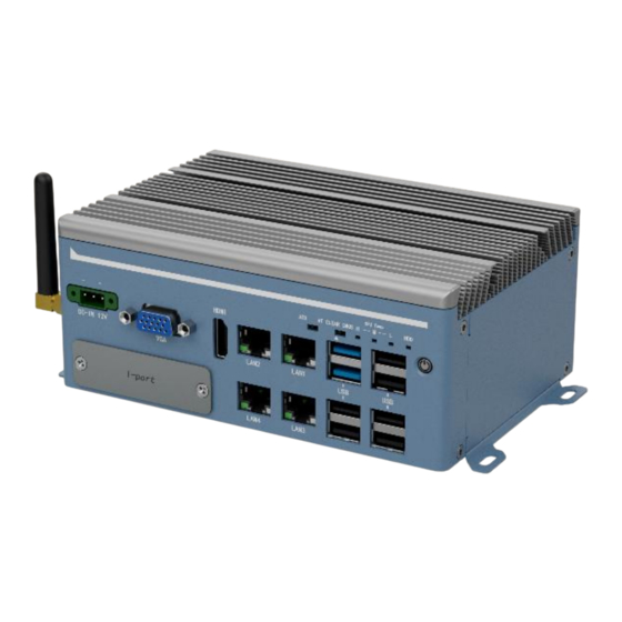
User’s Manual 1.5 Ordering Information Model No. Introduction 1*DDR4 SODIMM, 4*LAN, 2*USB3.1, 6*USB2.0, KMDA-2630/S001 Intel® Celeron J6412 4*COM, 8-bit DIO, 1*M.2, 1*Mini PCIe, 1*VGA, 1*HDMI, 1*Line out + 1*Line in + 1*Mic, 1*mSATA, KMDA-2630/S002 Intel® Celeron N6210 1*2.5”SATA bay, I-port, DC-IN 12V 1*DDR4 SODIMM, 4*LAN, 2*USB3.1, 6*USB2.0, KMDA-2630/S001/WP Intel®... - Page 14 User’s Manual 1*Power button 1*I-Port KMDA-2630-S Rear view: Figure 1. 2 I/O interface included on the rear panel: 1*8-bit DIO 2*RS232/422/485 2*RS232 1*Remote SW 1*Line out 1*Line in 1*Mic KMDA-2630-S Side view: Figure 1.
-
Page 15: Dimension
User’s Manual 1.7 Dimension KMDA-2630-S Series dimension(Unit:mm) Figure 1.4 ECM-I716(front) : Figure 1.5... - Page 16 User’s Manual ECM-I716(back) : Figure 1.6 ECB-277: Figure 1.7...
-
Page 17: Hardware Installation
User’s Manual Hardware Installation... -
Page 18: Introduction
User’s Manual 2.1 Introduction The following sections describe the panel dip switch setup and external connector and pin assignment for the product. 2.2 DIP switch setting KMDA-2630 fanless box computer is equipped with a simple DIP switch on the panel. This simple DIP switch can be toggled with tweezers or a card pin, which is convenient for users to set according to different configuration requirements. -
Page 19: At/Atx Power-On Mode Selection Switch
2.3 Connector Pin Assignments 2.3.1 Ethernet port(JLAN1, JLAN2) KMDA-2630-S Series is equipped with 2*Intel I226V (LAN1/2) + 2*Realtek 8111H (LAN3/4) chips through 4 RJ45 interfaces, and I226V Network port supports 10M/100M/1000M/2.5G rate self-adaption. The Ethernet provides a standard RJ-45 interface with LED indicators. Table 2.1 is a detailed pin assignment introduction. -
Page 20: Power Connector
User’s Manual LAN_DC-(GHz) RX-(10/100), LAN_DB-(GHz) LAN_DD+(GHz) LAN_DD-(GHz) Table 2.2 shows the connection rate represented by the LAN1/2 network port LED. Table 2.2: RJ-45 Led display state Type Left LED Right LED LED color Green Yellow 10 M cable Green fast blink 100M cable Green blink 1000M cable... -
Page 21: Cmos Battery
User’s Manual 2.3.3 CMOS battery KMDA-2630 provides CMOS battery interface through 1*2pin, 1.25mm terminal, the interface pin definition is as follows. Figure 2.5 CMOS battery interface Table 2.5:CMOS battery Port Pin Assignments Signal Signal BAT+ 2.3.4 Reset Port(RST) Figure 2.6 Reset Table 2.6 Reset Port Pin Assignments Signal Signal... -
Page 22: Sm Bus
User’s Manual Figure 2.8 8-bit DIO Table 2.8:DIO Port Pin Assignments Signal Signal DIO0 DIO4 DIO1 DIO5 DIO2 DIO6 DIO3 DIO7 2.3.7 SM Bus Figure 2.9 SM Bus Table 2.9:SMB Port Pin Assignments Signal Signal +V3.3 2.3.8 USB ports The front panel of KMDA-2630-S provides 2*USB3.1 Gen2 X1 Type A through a double-layer connector, with a transmission speed of up to 10G bit/sec;... -
Page 23: Hdmi
User’s Manual Table 2.10:USB3.1 type A Port Pin Assignments Signal Signal VBUS RX0+ TX0- TX0+ RX0- Shell Shield Table 2.11 shows the detailed pin assignment of USB2.0 Type A: Figure 2.11 USB2.0 Table 2.11: USB2.0 Port Pin Assignments Signal 2.3.9 HDMI The front panel of KMDA-2630 provides a high-resolution vertical HDMI display interface, the highest resolution supported can reach 4096 x 2304@60Hz, Table 2.12 is the detailed pin assignment introduction. -
Page 24: Vga Port
User’s Manual DATA0_N DATA2_N CLK_P DATA1_P CLK_N DETECT DATA1_N DATA0_P 2.3.10 VGA port The front panel of KMDA-2630 provides a VGA interface, which supports the maximum resolution of 1920*1200@60Hz. Table 2.13 shows the detailed pin assignment. Figure 2.13 VGA显示接口 Table 2.13: VGA Port Pin Assignments Signal Signal Signal... -
Page 25: B-Key 3052
User’s Manual 2.3.12 M.2 B-Key 3052 KMDA-2630 provides a M.2 B-Key 3052 with PCIe X1+USB2.0+SIM slot, which can support 5G NR or 4G LTE wireless routing module. Table 2.15 shows the specific pin assignments. Figure 2.14 M.2 B-Key插槽 Table 2.15: M.2 B-Key 3052 (NGFF1)Port Pin Assignments Signal Signal +V3_M2... -
Page 26: Com Ports
User’s Manual CLK_PCIe_P15 SIM_DET +3VS SUSCLK M.2_SSD_PEDET +V3_M2 +V3_M2 +V3_M2 2.3.13 COM ports The rear panel of KMDA-2630-S provides 2 RS232/422/485 serial ports (COM1, COM2) and 2 RS232 serial ports (COM3/COM4) through 4 DB9 single-row thin layers. Through BIOS setting, COM1/2 can be configured as RS232, RS422 or RS485. -
Page 27: Sata Port
User’s Manual Table 2.17: COM3/4 Port Pin Assignments Signal Signal 2.3.14 SATA port KMDA-2630 provides one SATA3.0 bay through one 7pin connectors, and the data transfer rate reaches 6Gb/s, which is used to connect SATA devices. Table 2.18 shows the detailed pin assignment of the SATA interface. -
Page 28: Msata Port
User’s Manual Signal Signal Warning: Make sure that Pin-1 of the SATA power connector has been inserted into the pin-1 of the corresponding plug to avoid damage to the board and hard drive! 2.3.16 mSATA port KMDA-2630 provides 1 mSATA slot and supports AHCI. The detailed pin assignment is as follows. Figure 2.18 mSATA port Table 2.20 mSATA Port Pin Assignments... -
Page 29: Front Panel
2.19 F-Panel Table 2.21:F_PANEL Port Pin Assignments Signal Signal HDD_LED+ PWR_SW#_C PWR_LED+ RST_SW# HDDLED- PWR_LED- SPK_OUT 2.3.18 Front Audio KMDA-2630-S series machine provides F_Audio interface through 2*5pin pins with 2.0mm pitch. The pin definitions are as follows. Figure 2.20 F-Audio port... -
Page 30: Jhctech Express-01 Composite Signal High-Speed Interface(Eio
GND_AUD 2.3.19 JHCTECH Express-01 Composite signal high-speed interface(EIO) KMDA-2630 provides the 80pin seismic high-speed signal interface of JHCTECH-01 E/IO high-speed interface specification through an 80pin connector, with 2*PCIeX1, 4*USB2.0, Front-Audio; 1*PS/2, Front-Panel, 1*Sm bus and 1*eSPI. The detailed pin assignment is as follows:... -
Page 31: Led
User’s Manual SIN4 DSR3# PCIE_WAKE- SIN3 DSR4# RTS3# DTR4# SOUT3 SOUT4 CTS3# PLTRST_N DTR3# POWERON RI3# SATA_LED# LPC_CLK PWR_LED LPC_AD0 GND_24 LPC_AD1 PWRBTN# LPC_AD2 RESET_IN# LPC_AD3 GPIO_8 LPC_SERIRQ GPIO_9 LPC_FRAME# GPIO_10 GND_69 GPIO_11 USB0_D+ GPIO_12 USB0_D- GPIO_13 GND_72 GND_33 USB1_D+/USB_SSTX+ SMB_CLK USB1_D-/USB_SSTX SMB_DAT... -
Page 32: Mini-Pcie
LEDs Working status warning Yellow high temperature Green Normal 2.3.21 Mini-PCIe KMDA-2630-S series machine provides one Mini-PCIe slot. Detailed pin allocation is shown in the following table. Figure 2.22 Mini-PCIe interface Table 2.25:Mini-PCIe Port Pin Assignments Signal Signal PCIE_WAKE_N +V3.3_MINICARD2 +V1.5... -
Page 33: Installation
User’s Manual PCIE_MINI_TX2+ +V3.3_MINICARD2 +V3.3_MINICARD2 +V1.5 +V3.3_MINICARD2 2.4 Installation 2.4.1 Install or replace the HDD/SDD Step 1: Unscrew the four screws near the bottom cover of the machine body and remove the bottom cover. Figure 2.4.1... - Page 34 User’s Manual Figure 2.4.2 Step 2: Remove the original SATA disk cable. Figure 2.4.3 Step 3: Unscrew the four screws on the hard disk tray and remove the hard disk tray. Figure 2.4.4 Step 4: Unscrew the four screws fastening the hard disk, remove the original hard disk, install the new HDD/SSD disk in the hard disk tray, and tighten the four screws respectively to secure the hard disk.
-
Page 35: Install The Ofx-075 Wide-Voltage Power Module
User’s Manual Figure 2.4.5 Step 5: Tighten the four screws on the hard disk tray with a hard disk in step three to secure the hard disk tray to the bottom cover. Step 6: Install bottom cover and tighten 4 screws according to Step 1. 2.4.2 Install the OFX-075 wide-voltage power module Tips: If you want to install the OFX-075 wide voltage power supply module, you need to remove the R3H2 resistor on the motherboard. - Page 36 User’s Manual hard disk bottom cover assembly. Step 2: Unscrew the four screws on the front panel and remove the front panel. Figure 2.4.7 Figure 2.4.8 Figure 2.4.9 Step 3: Unscrew a total of 12 screws on the rear panel, and remove the rear panel.
- Page 37 User’s Manual Figure 2.4.10 Figure 2.4.11 Figure 2.4.12 Step 4: Unscrew the four screws fixing the sub-card as shown in the figure and remove the sub-card.
- Page 38 User’s Manual Figure 2.4.13 Step 5: Install the OFX-075 wide voltage power module upside down at the position shown in the figure, and tighten two screws to fix the power module. Figure 2.4.14...
-
Page 39: Installing Memory Modules
User’s Manual Figure 2.4.15 Figure 2.4.16 Step 6: According to the disassembly steps, complete the installation of the bottom cover with the reverse disassembly method. 2.4.3 Installing Memory Modules Step 1: Remove the bottom cover, front and rear panels and subcards as in Steps 1, 2, 3 and 4 of 2.4.2. - Page 40 User’s Manual Figure 2.4.17 Step 4: Unscrew the 8 screws fixing the motherboard, and remove the motherboard. Figure 2.4.18 Step 5: Press the latches on both sides of the memory module and remove the original memory module from the mainboard. Take out the new memory module, align the gap, tilt the memory module 30 degrees, insert the memory module into the slot, and press down the memory module until the memory module is locked by the latches on both sides.
- Page 41 User’s Manual Figure 2.4.19 Step 6: Reinstall the specified thermal tape on the CPU and south bridge, then follow the disassembly steps and complete the product installation with the reverse steps. Figure 2.4.20...
-
Page 42: Bios Setup
User’s Manual BIOS Setup... -
Page 43: Bios Description
User’s Manual 3.1 BIOS Description BIOS is the communication bridge between hardware and software. How to correctly set the BIOS parameters is crucial for the system to work stably and whether the system works at its best. This chapter describes how to change the system settings through the BIOS settings. Note: For the purpose of better product maintenance, the manufacture reserves the right to change the BIOS items presented in this manual. - Page 44 User’s Manual...
-
Page 45: Bios Parameter Settings
User’s Manual 3.2 BIOS parameter settings When you start the Setup Utility, the main menu appears. The main menu of the Setup Utility displays a list of the options that are available. A highlight indicates which option is currently selected. Use the cursor arrow keys to move the highlight to other options. -
Page 46: Main Menu
User’s Manual 3.2.2 Main Menu When you enter the BIOS Setup program, the main menu appears, giving you an overview of the basic system information. Select an item and press <Enter> to display the submenu. Press <Esc> to back to the main menu. - Page 47 User’s Manual BIOS Information This item shows the information of the BIOS vendor, version, build date and time etc. Processor Information This item shows the basic information about the currently used processor, including name, type, speed, ID, core, Microcode version, etc. Total Memory This item shows the total memory size of the current motherboard.
-
Page 48: Advanced Menu
User’s Manual This item shows the basic information about PCH, including name, model, type, etc. System Language Set the language interface of the BIOS. System Date Set the date. The format of the date is <week><month><day><year>. System Time Set the time. The format of the time is <hour><minute><second>. 3.2.3 Advanced Menu This page sets up more advanced information about your system. - Page 49 User’s Manual CPU-Power Management Control This item contains the CPU-Power management control configuration, enter this sub-menu, there will be detailed details of the CPU-Power Management Control, as well as related settings of the CPU-Power Management Control function. Boot performance mode Boot performance mode settings, enter this sub-menu, there will be set boot performance mode: Max Battery, Max Non-Turbo Performance, Turbo Performance.
- Page 50 User’s Manual Turbo Mode Turbo mode settings, enter this sub-menu, you can choose whether to set it to turbo mode.
- Page 51 User’s Manual Platform PL1 Enable If Platform PL1 is enabled, you can manually limit CPU power consumption at Platform PL1 Power. Trusted Computing Trusted computing, enter this sub-menu, there will be the setting of the encryption security module (the motherboard will install the encryption module hardware will take effect). ACPI Settings Advanced configuration and power management interface settings, enter this submenu, there will be ACPI related settings.
-
Page 52: Chipset Menu
User’s Manual Hardware Monitor Hardware monitoring, enter this sub-menu, there will be CPU temperature, fan speed, status display of each common working voltage, as well as parameter settings of intelligent fan control. USB Configuration This item contains the USB configuration, enter this sub-menu, there will be detailed details of the USB, as well as related settings of the USB. - Page 53 User’s Manual System Agent (SA) Configuration System agent configuration menu,enter this submenu, there will be system agent configuration related settings. PCH-IO Configuration (South Bridge Configuration) PCH-IO configuration menu, enter this submenu, there will be PCH-IO configuration related settings. State After G3 State After G3 related settings, you can select S0 State or S5 State.
-
Page 54: Security Menu
User’s Manual 3.2.5 Security menu Administrator Password This item sets the information of the administrator password. User Password This item sets the information of the normal user password. Secure Boot This item sets the information of the secure boot.Secure Boot feature is Actice if Secure Boot is Enabled,Platform key(PK) is enrolled and mode change requires platform reset. -
Page 55: Boot Menu
User’s Manual 3.2.6 Boot menu Setup Prompt Timeout Setup prompts for waiting time. This option is to set the time to wait for the Del key to enter the BIOS setup after booting. Bootup NumLock State Set the state of the small numeric keypad at startup. Quiet Boot Switch full screen logo control. -
Page 56: Save & Exit Menu
User’s Manual 3.2.7 Save & Exit menu Save changes and Exit; This item enables you to save the changes that you have made and exit. Discard Changes and Exit; This item enables you to discard the changes that you have made and exit. Save Changes and Reset;... -
Page 57: Updating The Bios
User’s Manual 3.3 Updating the BIOS The BIOS (Basic Input and Output System) Setup Utility displays the system’s configuration status and provides you with options to set system parameters. The parameters are stored in battery-backed-up CMOS RAM that saves this information when the power is turned off. When the system is turned back on, the system is configured with the values you stored in CMOS. -
Page 58: Driver Installation
User’s Manual Driver Installation... -
Page 59: Follow The Sequence Below To Install The Drivers
User’s Manual The KMDA-2630 comes with a CD-ROM that contains all drivers and utilities that meet your needs. 4.1 Follow the sequence below to install the drivers: Figure 4.1 Step 1 – Install Chipset Driver Step 2 – Install Graphic Driver Step 3 –... -
Page 60: Utility Software Reference
User’s Manual 4.3 Utility Software Reference All the utility software available from this page is Windows compliant. They are provided only for the convenience of the customer. The following software is furnished under license and may only be used or copied in accordance with the terms of the license. -
Page 61: System Resource
User’s Manual SYSTEM RESOURCE... -
Page 62: Wdt And Gpio
User’s Manual 5.1 WDT and GPIO /* ====================================================================== * void jhctech_init(); * function description: library initializated, This function must be called before calling other functions * parameter description: * creation date: 5*======================================================================*/ /* ====================================================================== * void jhctech_deinit(); * function description: library release, Pair with jhctech_init, release the library's occupied resources when not needed * parameter description:... - Page 63 User’s Manual 5*========================================================================*/ /*========================================================================== 1 * void MB_gpio_output(WORD port,BYTE value); 2 * function description:The motherboard outputs high and low levels 3 * parameter description: parameter:port is the GPIO port of the main board, which is a fixed value designed by the manufacturer Level 8 bit of a bit, each bit controls a GPIO pin output value, Bit =1, means output high level...
- Page 64 User’s Manual 4 * creation date: 5*=======================================================================*/ Note: If you want more programs of the motherboard’s watchdog and GPIO, please call +86-0755-86021176-(8021)/+86-0755-86021176-(8023) for more information.
Need help?
Do you have a question about the KMDA-2630-S Series and is the answer not in the manual?
Questions and answers