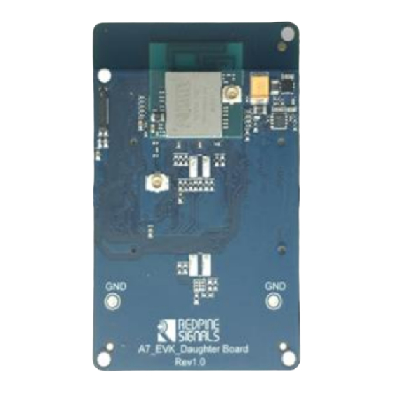
Summary of Contents for Silicon Laboratories AN1342
- Page 1 AN1342: RS9116 CC1 Board Layout Guidelines Version 1.1 August 20, 2021 silabs.com | Building a more connected world. 1 | Page...
-
Page 2: Table Of Contents
AN1342: RS9116 CC1 Board Layout Guidelines Version 1.1 Table of Contents Introduction .................................. 3 Placement Guidelines ..............................4 Antenna Layout Guidelines ............................5 SDIO/SPI Layout Guidelines ............................7 USB Layout Guidelines ............................... 9 UART Layout Guidelines ............................10 Power Supply Layout Guidelines ..........................11 GND Layout Guidelines ............................ -
Page 3: Introduction
AN1342: RS9116 CC1 Board Layout Guidelines Version 1.1 1 Introduction This Application Note provides PCB layout guidelines for the RS9116 CC1 module. These guidelines cover parts placement, various critical traces routing like RF, Host interfaces routing like SDIO/SPI, USB, UART, power routing, and GND pour. -
Page 4: Placement Guidelines
AN1342: RS9116 CC1 Board Layout Guidelines Version 1.1 2 Placement Guidelines Here are the recommendations for the placement of the CC1 module and its associated parts. Parts are placed on the same side of the CC1 module, in this Application Note. However, designers can choose to place them on either side of PCB for achieving best placement and routing. -
Page 5: Antenna Layout Guidelines
AN1342: RS9116 CC1 Board Layout Guidelines Version 1.1 3 Antenna Layout Guidelines The CC1 module has an integrated PCB trace antenna, and it works at both 2.4 GHz and 5 GHz. This antenna must be positioned toward outer periphery of the PCB edge. There is also a U.FL connector on the module, through which an external antenna can be connected. - Page 6 AN1342: RS9116 CC1 Board Layout Guidelines Version 1.1 Figure 3: U.FL Connector Details silabs.com | Building a more connected world. 6 | Page...
-
Page 7: Sdio/Spi Layout Guidelines
AN1342: RS9116 CC1 Board Layout Guidelines Version 1.1 4 SDIO/SPI Layout Guidelines SDIO and SPI are high speed interfaces where-in clock signals can reach up to 100 MHz. High speed design guidelines like below must be followed for the signals in these interfaces. SDIO/SPI signals include SDIO_CLK/SPI_CLK, SDIO_CMD/SPI_CSN, SDIO_D0/SPI_MOSI, SDIO_D1/SPI_MISO, SDIO_D2/SPI_INTR, SDIO_D3. - Page 8 AN1342: RS9116 CC1 Board Layout Guidelines Version 1.1 Since SDIO_CMD/SPI_CSN, SDIO_D1/SPI_MISO, SDIO_D3 signals are present on the inner row pins of the module, these must be routed in Layer 4 as shown below. SDIO_D3 SDIO_D1/ SDIO_CMD/ SPI_CSN SPI_MISO Figure 5: SDIO/SPI Signals Routing in Layer 4 silabs.com | Building a more connected world.
-
Page 9: Usb Layout Guidelines
AN1342: RS9116 CC1 Board Layout Guidelines Version 1.1 5 USB Layout Guidelines USB signals can reach speeds of 480 Mbps. Guidelines for the differential signals USB_DP and USB_DM must be followed. 1. It is highly recommended that the two USB differential signals (USB_DP and USB_DN) be routed in parallel with a spacing (i.e., a) that achieves 90 Ω... -
Page 10: Uart Layout Guidelines
AN1342: RS9116 CC1 Board Layout Guidelines Version 1.1 6 UART Layout Guidelines The guidelines below must be followed for UART signals. The signals are UART1_TX, UART1_RX, UART1_RTS, UART1_CTS. 1. Keep the UART signals away from noisy sources or other sensitive signals. -
Page 11: Power Supply Layout Guidelines
AN1342: RS9116 CC1 Board Layout Guidelines Version 1.1 7 Power Supply Layout Guidelines There are many power pins on the CC1 module. Careful routing with appropriate trace widths must be followed for better power delivery to the module. Follow the guidelines below for all the power traces. - Page 12 AN1342: RS9116 CC1 Board Layout Guidelines Version 1.1 The image below shows some of the Power Supply traces routing in Layer 3. As shown, they are routed in Star fashion from the supply source. VOUTLDOSOC Star routing UULP_VOUTSCDC Routing 3V3/1.85/VBATT...
-
Page 13: Gnd Layout Guidelines
AN1342: RS9116 CC1 Board Layout Guidelines Version 1.1 8 GND Layout Guidelines All the returns paths of critical signals like RF, high speed signals like SPI/SDIO/USB and Power, flow through GND. So, GND carries lot of return currents and high speed signals. Designer must ensure return paths are short. There are various possible ways to achieve good grounding, and below guidelines provide some of the possible insights into it. - Page 14 AN1342: RS9116 CC1 Board Layout Guidelines Version 1.1 The following image shows the example picture of GND pour in Layer 1 with one just via. Such hanging GND pour must be avoided. Stitch GND vias near the periphery of the GND pour, or else restrict such GND pour shapes.
-
Page 15: Revision History
AN1342: RS9116 CC1 Board Layout Guidelines Version 1.1 9 Revision History Revision No Version No Date Changes Jun, 2021 Initial version Aug, 2021 Added Figures titles and numbers silabs.com | Building a more connected world. 15 | Page... - Page 16 AN1342: RS9116 CC1 Board Layout Guidelines Version 1.1 silabs.com | Building a more connected world. 16 | Page...

Need help?
Do you have a question about the AN1342 and is the answer not in the manual?
Questions and answers