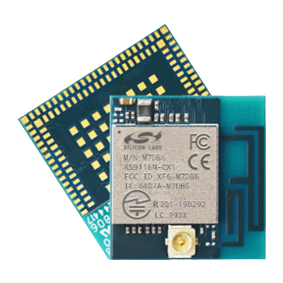
Summary of Contents for Silicon Laboratories RS9116
- Page 1 AN1344: RS9116 QMS Board Layout Guidelines Version 1.0 August 24, 2021 silabs.com | Building a more connected world. 1 | Page...
-
Page 2: Table Of Contents
AN1344: RS9116 QMS Board Layout Guidelines Version 1.0 Table of Contents Introduction ................................3 Placement Guidelines ............................... 4 RF Layout Guidelines ..............................6 Crystal Layout Guidelines ............................8 SDIO/SPI Layout Guidelines ............................. 9 USB Layout Guidelines ............................10 UART Layout Guidelines ............................11 Power Supply Layout Guidelines ........................... -
Page 3: Introduction
Version 1.0 1 Introduction This Application Note provides PCB layout guidelines for designing a PCB using the RS9116 QMS SoC. These guidelines cover parts placement, routing of various critical traces like RF, host interfaces routing like SDIO/SPI, USB, UART, power routing, and GND pour. -
Page 4: Placement Guidelines
AN1344: RS9116 QMS Board Layout Guidelines Version 1.0 2 Placement Guidelines The designer can choose a suitable antenna as per the product needs, like a chip antenna, on-board PCB trace, external PCB trace, dipole, etc. The design described in this Application Note uses a chip antenna. - Page 5 AN1344: RS9116 QMS Board Layout Guidelines Version 1.0 Considering the above recommendations, the QMS SoC and its circuitry can be placed on a single side of the PCB as shown below. This takes less than 25 mm x 20 mm of board space approximately, until RF antenna tuning network. The designer can choose to place the components better than what is shown below to suit the product needs.
-
Page 6: Rf Layout Guidelines
AN1344: RS9116 QMS Board Layout Guidelines Version 1.0 3 RF Layout Guidelines RF parts placement and trace routing affect the RF performance of the SoC and circuitry. Great care must be taken to ensure best design practices and the guidelines below are followed. - Page 7 AN1344: RS9116 QMS Board Layout Guidelines Version 1.0 The image below shows the overlap of RF routing on Top layer and the GND plane in the second layer. As can be observed, the entire RF circuitry has the second layer as GND reference. GND vias around RF circuitry are stitched directly to the GND plane.
-
Page 8: Crystal Layout Guidelines
AN1344: RS9116 QMS Board Layout Guidelines Version 1.0 4 Crystal Layout Guidelines Crystal placement and traces routing affect the crystal performance, and hence the start-up of the SoC after power on. The designer must ensure best design practices and guidelines below are followed. -
Page 9: Sdio/Spi Layout Guidelines
AN1344: RS9116 QMS Board Layout Guidelines Version 1.0 5 SDIO/SPI Layout Guidelines SDIO and SPI are high speed interfaces where-in clock signals can reach up to 100 MHz. High speed design guidelines like below must be followed for the signals in these interfaces. SDIO/SPI signals include SDIO_CLK/SPI_CLK, SDIO_CMD/SPI_CSN, SDIO_D0/SPI_MOSI, SDIO_D1/SPI_MISO, SDIO_D2/SPI_INTR, SDIO_D3. -
Page 10: Usb Layout Guidelines
7xa be maintained for high-speed periodic signals. 3. It is recommended that the total trace length of the signals between RS9116 part and USB connector (or USB host part) be less than 450 mm. -
Page 11: Uart Layout Guidelines
AN1344: RS9116 QMS Board Layout Guidelines Version 1.0 7 UART Layout Guidelines Below guidelines must be followed for UART signals. The signals are UART1_TX, UART1_RX, UART1_RTS, UART1_CTS. 1. Keep the UART signals away from noisy sources or other sensitive signals. -
Page 12: Power Supply Layout Guidelines
AN1344: RS9116 QMS Board Layout Guidelines Version 1.0 8 Power Supply Layout Guidelines There are many power pins on the QMS SoC. Careful routing with appropriate trace widths must be followed for better power delivery to the module. Follow the guidelines below for all the power traces. - Page 13 AN1344: RS9116 QMS Board Layout Guidelines Version 1.0 The image below shows example layout of Internal Buck regulator’s Power Supply traces routing in Layer 1. VOUTBCKDC VINLDOSOC INDUCTOR 1uH Ground Vias Isolation Ground under inductor VINBCKDC Input Cap VOUTBCKDC Cap...
- Page 14 AN1344: RS9116 QMS Board Layout Guidelines Version 1.0 The image below shows some of the Power Supply traces routing in Layer 3. As shown, they are routed in Star fashion from the supply source. VOUTLDO1P8 VOUTLDOSOC Star routing VOUTBCKC Star routing...
- Page 15 AN1344: RS9116 QMS Board Layout Guidelines Version 1.0 The image below shows Power Supply traces routing in Layer 4. As shown, they are routed in Star fashion from the supply source. VOUTLDOAFE 3.3V/1.85V/ VBATT Star routing Figure 10: Power Supply Routing in Layer 4 silabs.com | Building a more connected world.
-
Page 16: Gnd Pour Layout Guidelines
AN1344: RS9116 QMS Board Layout Guidelines Version 1.0 9 GND Pour Layout Guidelines All the returns paths of critical signals like RF, high speed signals like SPI/SDIO/USB and power, flow through GND. So, GND carries lot of return currents and high speed signals. Designer must ensure return paths are short. There are various possible ways to achieve good grounding, and below guidelines provide some of the possible insights into it. - Page 17 AN1344: RS9116 QMS Board Layout Guidelines Version 1.0 The image below shows the example picture of GND pour in Layer 1 with one just via. Such hanging GND pour must be avoided. Stitch GND vias near the periphery of the GND pour, or else restrict such GND pour shapes.
- Page 18 AN1344: RS9116 QMS Board Layout Guidelines Version 1.0 silabs.com | Building a more connected world. 18 | Page...


Need help?
Do you have a question about the RS9116 and is the answer not in the manual?
Questions and answers