
Related Manuals for Advantech AIMB-277


Summary of Contents for Advantech AIMB-277
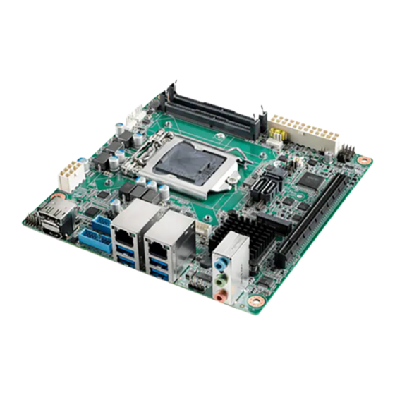
- Page 1 User Manual AIMB-277 Intel® Core™ i9/i7/i5/i3/Pentium/ Celeron LGA1200 Mini-ITX with HDMI/DP/VGA/LVDS (or eDP), 2 COM & 8 USB, 2 LAN, and M.2 E/M key...
- Page 2 No part of this manual may be reproduced, copied, translated or transmitted in any form or by any means without the prior written permission of Advantech Co., Ltd. Information provided in this manual is intended to be accurate and reliable. How- ever, Advantech Co., Ltd.
- Page 3 Advantech has come to be known. Your satisfaction is our primary concern. Here is a guide to Advantech’s cus- tomer services.
- Page 4 SNEFB AQD- SEC019 AQD- DDR4 3200 32GB Advantech SD4U32GN32- K4AAG08 SD4U32GN3 PASS 5WABCWE 2-SB SEC 552 AQD- AQD- BCPB DDR4 2133 Advantech SD4U8GN21- SD4U8GN21 PASS K4A4G085W AQD- SEC001 AQD- DDR4 3200 Advantech SD4U8GN32- K4A8G08 SD4U8GN32 PASS 5WCBCWE AIMB-277 User Manual...
- Page 5 TPM AMP /eDP 2.0a AIII 2 Gen2 2 Gen1 AIMB-277G2- Q470E 1 / (1) 1 FLA1E AIMB-277G2- Q470E 0 / (1) 0 00A1E *() Supports by BOM options Note! USB power current delivery under S5 Max. 1.8A. AIMB-277 User Manual...
- Page 6 It should be free of marks and scratches and in perfect working order upon receipt. As you unpack the AIMB-277, check it for signs of ship- ping damage. (For example, damaged box, scratches, dents, etc.) If it is damaged or it fails to meet the specifications, notify our service department or your local sales representative immediately.
-
Page 7: Table Of Contents
Figure 1.1 Jumper and Connector Location (Top Side)....5 Figure 1.2 Jumper and Connector Location (Bottom Side) ..6 AIMB-277 Board Diagram ................. 6 Figure 1.3 AIMB-277 Board Diagram .......... 6 Safety Precautions ..................7 Jumper Settings ..................7 1.8.1 How to Set Jumpers.............. - Page 8 Windows® 10 Driver Setup (Intel i219LM&Intel i211AT) ....... 79 Appendix A I/O Pin Assignments ......81 Connector and Header List Description: ..........82 A.1.1 SYSTEM FAN Power Connector (SYSFAN1) ......82 Table A.1: SYSTEM FAN Power Connector (SYSFAN1)..82 AIMB-277 User Manual viii...
- Page 9 Table A.26:SYSTEM FAN Power Connector (SYSFAN2) ..99 A.1.28 DDR4 SO-DIMM Socket (DIMMB1)..........99 A.1.29 DDR4 SO-DIMM Socket(DIMMA1)..........99 A.1.30 NGFF M.2 E-Key connector for 2242 module (M2E1)....99 Table A.27:NGFF M.2 E-Key conn for 2242 module (M2E1) ... 100 AIMB-277 User Manual...
- Page 10 AIMB-277 User Manual...
-
Page 11: Chapter 1 General Information
Chapter General Information... -
Page 12: Introduction
Introduction AIMB-277 is designed with the Intel® Q470E PCH for industrial applications that require both performance computing and enhanced power management capabilities. The motherboard supports Intel desktop Corei9/i7/i5/i3/Pentium/Celeron processors, up to 20 MB SmartCache, and 2 x DDR4 2933MHz SO-DIMM, up to 64 GB. Multiple I/O connectivity of 2 x serial ports, 4 x USB 3.2 Gen 2 + 4 x USB 3.2 Gen 1, 2 x GbE... -
Page 13: Graphics
Power supply voltage: +3.3V, +5V, +12V, -12V, +5VSB Power consumption: Intel Core i9-10900E 2.8GHz, 2pcs 32GB DDR4 3200MHz SDRAM, Boost: 117.882W; Typical: 102W Board size: 170 mm x 170 mm (6.69" x 6.69"). Board weight: 0.365 kg. AIMB-277 User Manual... -
Page 14: Jumpers And Connectors
Jumpers and Connectors Connectors on the AIMB-277 motherboard link it to devices such as hard disk drives and a keyboard. In addition, the board has a number of jumpers used to configure the system for your application. The tables below list the function of each of the board jumpers and connectors. Later sections in this chapter give instructions on setting jumpers. -
Page 15: Board Layout: Jumper And Connector Locations
USB78 JLVDS_VCON3 LVDS_EDP3 INV3 JLVDS3 PCIEX16 ATX12V1 M2M1 COM12 SATA1 CPU1 SATA3 SATA2 CPUFAN1 SPI1 ESPI1 JFP2 JCMOS1 BAT1 SYSFAN1 SYSFAN2 PSON1 GPIO1 JCASE2 DIMMB1 DIMMA1 EATXPWR1 JWDT1+JOBS1 JFP1 Figure 1.1 Jumper and Connector Location (Top Side) AIMB-277 User Manual... -
Page 16: Aimb-277 Board Diagram
3 SATAIII SATA III USB2.0 PCIe x4 (Gen2) M.2_M Socket (Storage) M.2_E Socket (WiFi) PCIe x1 SATA III eSPI ALC 888S SPI 256MB BIOS Super I/O Nuvuton TPM 2.0 HD Audio 2 RS-232/422/485 Figure 1.3 AIMB-277 Board Diagram AIMB-277 User Manual... -
Page 17: Safety Precautions
1, 2, and 3. In this case you connect either pins 1 and 2, or 2 and 3. A pair of needle-nose pliers may be useful when set- ting jumpers. AIMB-277 User Manual... -
Page 18: Cmos Clear (Jcmos1)
1.8.2 CMOS Clear (JCMOS1) The AIMB-277 motherboard contains a jumper that can erase CMOS data and reset the system BIOS information. Normally this jumper should be set with pins 1-2 closed. If you want to reset the CMOS data, set CMOS1 to 2-3 closed for just a few seconds, and then move the jumper back to 1-2 closed. -
Page 19: Lvds/Edp Panel Voltage Selection (Jlvds3)
Jumper position for +12V 1.8.6 LVDS VESA, JEIDA Format Selection Pin Header (JLVDS_VCON3) Table 1.6: LVDS VESA, JEIDA Format Selection Pin Header (JLVDS_VCON3) Function Jumper Setting JEIDA mode Setting: +V3.3 VESA mode Setting: GND (Default) Signal Pin Definition +3.3V LVDS1_VCON AIMB-277 User Manual... -
Page 20: System Memory
System Memory AIMB-277 has two sockets for a 260-pin DDR4 SO-DIMM. These sockets use a 1.2 V unbuffered double data rate synchronous DRAM (DDR SDRAM). DRAM is available in capacities of 4GB, 8GB, 16GB and 32GB. The sockets can take any combination with SODIMMs of any size, giving a total memory size between 4GB, 8GB, 16GB, and up to max 64GB. -
Page 21: Chapter 2 Connecting Peripherals
Chapter Connecting Peripherals... -
Page 22: Introduction
ATX 12V Power Supply Connector (ATX12V1) & ATX Power Supply Connector (EATXPWR1) Signal Pin Definition +12V +12V +12V +12V Signal Pin Definition Signal Pin Definition +3.3V_1 +3.3V_4 +3.3V_2 -12V COM_1 COM_4 +5V_1 PS_ON# COM_2 COM_5 +5V_2 COM_6 COM_3 COM_7 PWR_OK AIMB-277 User Manual... -
Page 23: Displayport+ High Definition Multimedia Interface (Dp1+Hdmi1)
+5VSB +5V_3 +12V1_1 +5V_4 +12V1_2 +5V_5 +3.3V_3 COM_8 DisplayPort+ High Definition Multimedia Interface (DP1+HDMI1) AIMB-277 User Manual... -
Page 24: Lan1_Usb12 + Lan2_Usb34, Usb56, Usb78
LAN1_USB12 + LAN2_USB34, USB56, USB78 The AIMB-277 provides up to eight USB ports. Four USB3.2 Gen2 on the rear side and two pin header on the board. The USB interface complies with USB specification Rev. 2.0 and Rev. 3.0 supporting transmission rates up to 10 Gbps for USB1234, and up to 5Gbps for USB5678. -
Page 25: Vga Connector (Vga1)
VGA connector (VGA1) Signal Pin Definition VGA1_b_R VGA1_a_DCLK VGA1_b_G VGA1_FOC_ON VGA1_b_B VGA1_a_DDAT VGA1_b_VS VGA1_b_HS +VCC_TMDS AIMB-277 User Manual... -
Page 26: Hd Analog Audio Interface (Audio1)
HD Analog Audio Interface (Audio1) Amplifier Connector (AMP1) Signal Pin Definition SPK_R+ SPK_R- SPK_L- SPK_L+ AIMB-277 User Manual... -
Page 27: Ngff M.2 M-Key Connector For 2280 Module (M2M1)
NGFF M.2 M-Key Connector for 2280 Module (M2M1) AIMB-277 User Manual... -
Page 28: Ngff M.2 E-Key Connector For 2230 Module (M2E1)
NGFF M.2 E-Key Connector for 2230 Module (M2E1) 2.10 LVDS/eDP Connector (LVDS_EDP3) AIMB-277 User Manual... -
Page 29: Lvds Backlight Inverter Power Connector (Inv3)
LVDS Backlight Inverter Power Connector (INV3) 2.12 Serial ATA Interface Connector (SATA1/2/3) AIMB-286EF features a high performance Serial ATA III interface (up to 600 MB/s) which eases hard drive cabling with thin, space-saving cables. SATA3 SATA1 SATA2 Signal AIMB-277 User Manual... -
Page 30: Espi Interface Connector (Espi1)
2.13 eSPI Interface Connector (ESPI1) AIMB-277 User Manual... -
Page 31: 8-Bit General Purpose I/O Pin Header (Gpio1)
2.14 8-bit General Purpose I/O Pin Header (GPIO1) 2.15 COM Port Pin Header (COM12) Signal Pin Definition Signal Pin Definition COM1_422_485_TX- COM1_DSR# COM1_422_485_TX+ COM1_RTS# COM1_422_RX+ COM1_CTS# COM1_422_RX- COM1_RI# AIMB-277 User Manual... -
Page 32: Case Open Connector (Jcase2)
COM2_422_485_TX- COM2_DSR# COM2_422_485_TX+ COM2_RTS# COM2_422_RX+ COM2_CTS# COM2_422_RX- COM2_RI# 2.16 Case Open Connector (JCASE2) Signal Case Open AIMB-277 User Manual... -
Page 33: Pci Express X16 Slot (Pciex16_1)
2.17 PCI Express X16 Slot (PCIEX16_1) AIMB-277 provides 1 x PCI express x16 slot. 2.18 Power LED Pin Header (JFP2) Signal Pin Definition SIO_SUSLED_R SIO_SUSLED AIMB-277 User Manual... -
Page 34: Spi Bios Flash Socket (Spi1)
2.19 SPI BIOS Flash Socket (SPI1) 2.20 Power Switch/HDD LED/SMBUS/Speaker Pin Header (JFP1) Signal Pin Definition Signal Pin Definition FP_HDD_LED PWR_BTN FP_HDD_LED# SMB_DAT_JFP1 FP_SYS_RESET# SMB_CLK_JFP1 AIMB-277 User Manual... -
Page 35: System Fan #1 Connector /System Fan #2 Connector (Sysfan1/2)
If a fan is used, this connector supports cooling fans of 500 mA (6 W) or less. SYSFAN1 SYSFAN2 2.22 CPU FAN Connector (CPUFAN1) If a fan is used, this connector supports cooling fans of 500 mA (6 W) or less. AIMB-277 User Manual... -
Page 36: Cmos Battery Connector (Bat1)
2.23 CMOS Battery Connector (BAT1) 2.24 CPU Socket (CPU1) AIMB-277 User Manual... -
Page 37: Ddr4 So-Dimm Socket (Dimma1, Dimmb1)
2.25 DDR4 SO-DIMM Socket (DIMMA1, DIMMB1) DIMMA1 DIMMB1 AIMB-277 User Manual... - Page 38 AIMB-277 User Manual...
-
Page 39: Bios Operation
Chapter BIOS Operation... -
Page 40: Introduction
AIMB-277 setup screens. BIOS Setup The AIMB-277 Series system has AMI BIOS built in, with a CMOS SETUP utility that allows users to configure required settings or to activate certain system features. The CMOS SETUP saves the configuration in the CMOS RAM of the motherboard. When the power is turned off, the battery on the board supplies the necessary power to pre- serve the CMOS RAM. -
Page 41: Main Menu
System Date using the <Arrow> keys. Enter new values via the keyboard. Press the <Tab> or <Arrow> keys to move between fields. The date must be entered in MM/DD/YY format. The time must be entered in HH:MM:SS format. AIMB-277 User Manual... -
Page 42: Advanced Bios Features
3.2.2 Advanced BIOS Features Select the Advanced tab from the AIMB-277 setup screen to enter the Advanced BIOS Setup screen. You can select any of the items in the left frame of the screen, such as CPU Configuration, to go to the sub menu for that item. You can display an Advanced BIOS Setup option by highlighting it using the <Arrow>... - Page 43 3.2.2.1 Platform Misc Configuration Native PCIE Enable [Enable] Native ASPM [Auto] AIMB-277 User Manual...
- Page 44 3.2.2.2 CPU Configuration CPU Flex Ratio Override [Disabled] Intel (VMX) Virtualization [Enabled] Active Processor Cores [All] Hyper-Threading [Enabled] Intel Trusted Execution Technology [Disabled] Alias Check Request [Disabled] AIMB-277 User Manual...
- Page 45 3.2.2.3 Power & Performance CPU - Power Management Control AIMB-277 User Manual...
- Page 46 IO MWAIT Redirection [Disabled] Package C-state Limit [Auto] Time Unit [1024 ns] Thermal Monitor [Enabled] Interrupt Redirection Mode Selection [PAIR with Fixed Priority] Timed MWAIT [Disabled] Energy Performance Gain [Disabled] AIMB-277 User Manual...
- Page 47 Current Turbo Settings Energy Efficient P-state [Enabled] Package Power Limit MSR Lock [Disabled] Power Limit 1 Override [Enabled] Power Limit 1 Time Window [0] Power Limit 2 Override [Enabled] Energy Efficient Turbo [Auto] AIMB-277 User Manual...
- Page 48 Custom P-State Table GT - Power Management Control RC6 (Render Standby) [Enabled] Maximum GT frequency [Default Max Frequency] Disable Turbo GT frequency [Disabled] AIMB-277 User Manual...
- Page 49 3.2.2.4 PCH-FW Configuration ME State [Enabled] Manageability Features Stage [Enabled] AMT BIOS Features [Enabled] AMT Configuration Firmware Update Configuration USB Provisioning of AMT [Disabled] AIMB-277 User Manual...
- Page 50 CIRA Configuration Activate Remote Assistance Process [Disabled] ASF Configuration PET Progress [Enabled] WatchDog [Disabled] ASF Sensors Table [Disabled] AIMB-277 User Manual...
- Page 51 Secure Erase Configuration Secure Erase mode [Simulated] Force Secure Erase [Disabled] OEM Flags Settings MEBx Hotkey Pressed [Disabled] MEBx Selection Screen [Disabled] AIMB-277 User Manual...
- Page 52 Hide Unconfigured ME Confirmation Prompt [Disabled] MEBx OEM Debug Menu Enable [Disabled] Unconfigure ME [Disabled] MEBx Resolution Settings Non-UI Mode Resolution [Auto] UI Mode Resolution [Auto] Graphics Mode Resolution [Auto] AIMB-277 User Manual...
- Page 53 Firmware Update Configuration Me FW Image Re-Flash [Disabled] FW Update [Enabled] 3.2.2.5 Trusted Computing Security Device Support [Enabled] SHA-1 PCR Bank [Enabled] AIMB-277 User Manual...
- Page 54 Physical Presence Spec Version [1.3] TPM 2.0 InterfaceType [TIS] Device Select [Auto] 3.2.2.6 ACPI Settings Enable ACPI Auto Configuration [Disabled] Enable Hibernation [Enabled] ACPI Sleep State [S3 (Suspend to RAM) ] AIMB-277 User Manual...
- Page 55 3.2.2.7 NCT6796D Super IO Configuration Serial Port [Enabled] Change Settings [Auto] Device Mode [RS232] AIMB-277 User Manual...
- Page 56 Serial Port [Enabled] Change Settings [Auto] Device Mode [RS232] 3.2.2.8 NCT6796D HW Monitor Smart Fan Function [Enabled] CPU Warning Temperature [Disabled] AIMB-277 User Manual...
- Page 57 ACPI Shutdown Temperature [Disabled] Case Open Warning [Disabled] Wake On Ring [Disabled] Watch Dog Timer [Disabled] Smart Fan Function CPU Fan Mode [SMART FAN IV Mode] AIMB-277 User Manual...
- Page 58 Digital I/O Configuration Digital I/O Pin 1~8 [Input] 3.2.2.9 S5 RTC Wake Settings Wake system from S5 [Disabled] AIMB-277 User Manual...
- Page 59 3.2.2.10 Serial Port Console Redirection Console Redirection [Disabled] Console Redirection EMS [Disabled] Legacy Console Redirection Settings Redirection COM Port [COM1] Resolution [80x24] Redirect After POST [Always Enable] AIMB-277 User Manual...
- Page 60 3.2.2.11 Intel TXT Information 3.2.2.12 USB Configuration Legacy USB Support [Enabled] XHCI Hand-off [Enabled] USB Mass Storage Driver Support [Enabled] USB transfer time-out [20 sec] Device reset time-out [20 sec] AIMB-277 User Manual...
- Page 61 USB PWR OFF Configuration1 [Disabled] USB PWR OFF Configuration2 [Disabled] USB PWR OFF Configuration3 [Disabled] USB PWR OFF Configuration4 [Disabled] Note! USB power current delivery under S5 Max. 1.8A. 3.2.2.13 Network Stack Configuration Network Stack [Disabled] AIMB-277 User Manual...
- Page 62 3.2.2.14 CSM Configuration CSM Support [Disabled] 3.2.2.15 NVMe Configuration AIMB-277 User Manual...
-
Page 63: Chipset Configuration Setting
Users can display a Chipset Setup option by highlighting it using the <Arrow> keys. All Chipset Setup options are described in this section. The Chipset Setup screens are shown below. The sub menus are described on the following pages. AIMB-277 User Manual... -
Page 64: System Agent (Sa) Configuration
3.3.1 System Agent (SA) Configuration VT-d [Enabled] Above 4GB MMIO BIOS assignment [Disabled] DMA Control Guarantee [Disabled] AIMB-277 User Manual... - Page 65 3.3.1.1 Memory Configuration The item shows you memory specification included RC version, frequency, size and voltage information etc. Maximum Memory Frequency (Auto) Max TOLUD [ Dynamic ] Train On Warm boot [Disabled] AIMB-277 User Manual...
- Page 66 3.3.1.2 Graphics Configuration GTT size [8MB] Aperture Size [256MB] DVMT Pre-Allocated [32M] DVMT Total Gfx Mem [256M] PM Support [Enabled] PAVP Enable [Enabled] AIMB-277 User Manual...
- Page 67 3.3.1.3 LCD Control LVDS Panel Type [Disabled] eDP/LVDS Backlight Signal Control [LINEAR] LVDS Backlight PWM Frequency Control [23.47 KHz] AIMB-277 User Manual...
-
Page 68: Pch-I/O Configuration
3.3.2 PCH-I/O Configuration 3.3.2.1 PCI Express Configuration PCI Express Clock Gating [Enabled] PCIe-USB Glitch W/A [Disabled] AIMB-277 User Manual... - Page 69 M.2 M-key slot M.2 M-key slot [Enabled] ASPM 4 [Auto] L1 Substates [L1.1 & L1.2] Advanced Error Reporting [Enabled] PCIe Speed [Auto] LAN2 Controller AIMB-277 User Manual...
- Page 70 M.2 E-key slot M.2 E-key slot [Enabled] ASPM 11 [Auto] L1 Substates [L1.1 & L1.2] Advanced Error Reporting [Enabled] PCIe Speed [Auto] Extra options Detect Non-Compliance Device [ Disabled ] AIMB-277 User Manual...
- Page 71 Serial ATA Port 1 (SATA) Port 1 [Enabled ] Spin Up Device [ Disabled ] SATA Device Type [ Hard Disk Drive ] SATA Port 1 DevS1p [ Disabled] DITO Configuration [ Disabled ] AIMB-277 User Manual...
- Page 72 Serial ATA Port 3 (SATA) Port 3 [Enabled ] Spin Up Device [ Disabled ] SATA Device Type [ Hard Disk Drive ] SATA Port 3 DevS1p [ Disabled] DITO Configuration [ Disabled ] AIMB-277 User Manual...
- Page 73 3.3.2.3 Security Configuration RTC Memory Lock [Enabled] BIOS Lock [Enabled] AIMB-277 User Manual...
-
Page 74: Security
3.3.2.4 HD Audio Configuration HD Audio [Enabled] Security AIMB-277 User Manual... - Page 75 Administrator password. User Password Select this option and press <ENTER> to access the sub menu, and then type in the password to set the User Password. Secure Boot [ Enabled] Secure Boot Mode [Standard] AIMB-277 User Manual...
-
Page 76: Boot Setting
On or off power on state for the NumLock. Quiet Boot [Disabled] If this option is set to disabled, the BIOS displays normal POST messages. If enabled, an OEM logo is shown instead of POST messages. AIMB-277 User Manual... -
Page 77: Save & Exit Configuration
Restore Default Restore/Load default values for all the setup options. Save as User Default Save the changes done so far as user defaults. Restore User Default Restore the user defaults to all the setup options. AIMB-277 User Manual... - Page 78 AIMB-277 User Manual...
-
Page 79: Software Introduction & Service
Chapter Software Introduction & Service... -
Page 80: Introduction
Introduction The mission of Advantech Embedded Software Services is to "Enhance quality of life with Advantech platforms and Microsoft® Windows® embedded technology." We enable Windows® Embedded software products on Advantech platforms to more effectively support the embedded computing community. Customers are freed from the hassle of dealing with multiple vendors (hardware suppliers, system integrators, embedded OS distributors) for projects. - Page 81 (restarting the system) after a certain number of seconds. Hardware Monitor The Hardware Monitor (HWM) API is a system health super- vision API that inspects certain condition indexes, such as fan speed, temperature and voltage. AIMB-277 User Manual...
- Page 82 AIMB-277 User Manual...
-
Page 83: Chipset Software Installation Utility
Chapter Chipset Software Installation Utility... -
Page 84: Before You Begin
Before You Begin To facilitate the installation of the enhanced display drivers and utility software, read the instructions in this chapter carefully. The drivers for the AIMB-277 are located on the Advantech support website: http://support.advantech.com/Support/. The drivers on the support website will guide and link you to the utilities and drivers under a Win- dows system. -
Page 85: Vga Setup
Chapter VGA Setup... -
Page 86: Introduction
See Chapter 5 for information on installing the CSI util- ity. Download the driver from website on your computer. Navigate to the “AIMB- 277_Graphic_Win10 (64-bit)” folder and click “setup.exe” to complete the installation of the drivers for Windows 10. AIMB-277 User Manual... -
Page 87: Lan Configuration
Chapter LAN Configuration... -
Page 88: Introduction
Introduction The AIMB-277 has two Gigabit Ethernet LANs via dedicated PCI Express x1 lanes Intel i211AT and I219LM (Phi) that offer bandwidth of up to 500 MB/sec, eliminating the bottleneck of network data flow and incorporating Gigabit Ethernet at 1000 Mbps. -
Page 89: Windows® 10 Driver Setup (Intel I219Lm&Intel I211At)
Select the “Autorun” then navigate to the directory for your OS. Note! Before installing this driver, make sure the CSI utility has been installed in your system. See Chapter 5 for information on installing the CSI util- ity. AIMB-277 User Manual... - Page 90 AIMB-277 User Manual...
-
Page 91: Appendix A I/O Pin Assignments
Appendix I/O Pin Assignments... -
Page 92: Connector And Header List Description
Connector and Header List Description: A.1.1 SYSTEM FAN Power Connector (SYSFAN1) Table A.1: SYSTEM FAN Power Connector (SYSFAN1) Signal Pin Definition SYSTEM FAN VCC SYSTEM FAN SPEED SYSTEM FAN PWM A.1.2 CPU FAN Power Connector (CPUFAN1) Table A.2: CPU FAN Power Connector (CPUFAN1) Signal Pin Definition SYSTEM FAN VCC SYSTEM FAN SPEED... - Page 93 A.1.4 ATX 12V Power Supply Connector (ATX12V1) Table A.3: ATX 12V Power Supply Connector (ATX12V1) Signal Pin Definition +12V +12V +12V +12V A.1.5 VGA connector (VGA1) Table A.4: VGA connector (VGA1) Signal Pin Definition VGA1_b_R VGA1_a_DCLK VGA1_b_G VGA1_FOC_ON VGA1_b_B VGA1_a_DDAT VGA1_b_VS VGA1_b_HS +VCC_TMDS...
- Page 94 A.1.6 DisplayPort+ High Def Multimedia Interface (DP1+HDMI1) Table A.5: DisplayPort+ High Definition Multimedia Interface (DP1+HDMI1) Signal Pin Definition Signal Pin Definition HDMI2_Z_D2+ DP1_0+ HDMI2_Z_D2- DP1_0- HDMI2_Z_D1+ DP1_1+ HDMI2_Z_D1- DP1_1- HDMI2_Z_D0+ DP1_2+ HDMI2_Z_D0- DP1_2- HDMI2_Z_CLK+ DP1_3+ HDMI2_Z_CLK- DP1_3- A.1.7 USB 3.2 Gen1+2.0 pin header (USB56) Table A.6: USB 3.2 Gen1+2.0 pin header (USB56) Signal Pin Definition Signal Pin Definition...
- Page 95 Table A.6: USB 3.2 Gen1+2.0 pin header (USB56) USB31_P5_z_RX+ USB31_P6_z_TX+ USB31_P5_z_TX- USB31_P6_z_TX- USB31_P5_z_TX+ USB31_P6_z_RX+ USB2_D5- USB31_P6_z_RX- USB2_D5+ +USBV3 A.1.8 USB 3.2 Gen1+2.0 pin header (USB78) Table A.7: USB 3.2 Gen1+2.0 pin header (USB78) Signal Pin Definition Signal Pin Definition +USBV4 USB2_D8+ USB31_P7_z_RX- USB2_D8-...
- Page 96 A.1.9 eDP/LVDS Panel Connector (LVDS_EDP3) Table A.8: eDP/LVDS Panel Connector (LVDS_EDP3) Signal Pin Definition Signal Pin Definition +VDD_LVDS1 +VDD_LVDS1 LVDS_DET# +VDD_LVDS1 +VDD_LVDS1 LVDS1_A0N LVDS1_A4N LVDS1_A0P LVDS1_A4P LVDS1_A1N LVDS1_A5N LVDS1_A1P LVDS1_A5P LVDS1_A2N LVDS1_A6N LVDS1_A2P LVDS1_A6P LVDS1_CLK1N LVDS1_CLK2N LVDS1_CLK1P LVDS1_CLK2P LVDS1_SCD LVDS1_SDD LVDS1_A3N LVDS1_A7N LVDS1_A3P...
- Page 97 A.1.10USB 3.2 Gen2+RJ45 1 port (LAN2_USB34) Table A.9: USB 3.2 Gen2+RJ45 1 port (LAN2_USB34) Signal Pin Definition Signal Pin Definition LAN2_LED2_1G#_R +USBV2 LAN2_LED0_100M#_R USB2_D3- LAN2_VCT USB2_D3+ LAN2_MDI0+ LAN2_MDI0- USB31_P3_z_RX- LAN2_MDI1+ USB31_P3_z_RX+ LAN2_MDI1- LAN2_MDI2+ USB31_P3_z_TX- LAN2_MDI2- USB31_P3_z_TX+ LAN2_MDI3+ +USBV2 LAN2_MDI3- USB2_D4- LAN2_CT USB2_D4+ LAN2_LED1_ACT#_R...
- Page 98 A.1.11 USB 3.2 Gen2+RJ45 1 port (LAN1_USB12) Table A.10: USB 3.2 Gen2+RJ45 1 port (LAN1_USB12) Signal Pin Definition Signal Pin Definition LAN1_LED2_1G#_R +USBV1 LAN1_LED0_100M#_R USB2_D1- LAN1_VCT USB2_D1+ LAN1_MDI0+ LAN1_MDI0- USB31_P1_z_RX- LAN1_MDI1+ USB31_P1_z_RX+ LAN1_MDI1- LAN1_MDI2+ USB31_P1_z_TX- LAN1_MDI2- USB31_P1_z_TX+ LAN1_MDI3+ +USBV1 LAN1_MDI3- USB2_D2- LAN1_CT USB2_D2+...
- Page 99 A.1.12Audio amplifier output pin header (AMP1) Table A.11: Audio amplifier output pin header (AMP1) Signal Pin Definition SPK_R+ SPK_R- SPK_L- SPK_L+ A.1.13Front panel audio pin header (AUDIO1) Table A.12: Front panel audio pin header (AUDIO1) Signal Pin Definition GND_A A_z_MIC1-L GND_A A_MIC1-JD A_z_MIC1-R...
- Page 100 A.1.14LVDS backlight inverter power connector (INV3) Table A.13: LVDS Backlight inverter power connector (INV3) Signal Pin Definition +V12_INV1 INV1_ENBKL INV1_VBR +V5_INV1 A.1.15PCI Express X16 Slot (PCIEX16_1) Table A.14: PCI Express X16 Slot (PCIEX16_1) Signal Pin Definition Signal Pin Definition 12V_1 PRSNT1 AIMB-231 User Manual...
- Page 101 Table A.14: PCI Express X16 Slot (PCIEX16_1) 12V_2 12V_4 12V_3 12V_5 GND_1 GND_3 SMCLK JTAG2 SMDAT JTAG3 GND_2 JTAG4 3_3V_1 JTAG5 JTAG1 3_3V_2 3_3VAUX 3_3V_3 WAKE PWRGD RSVD_1 GND_7 GND_4 REFCLK+ HSOP0 REFCLK- HSON0 GND_8 GND_5 HSIP0 PRSNT2_1 HSIN0 GND_6 GND_9 HSOP1 RSVD_3...
- Page 102 Table A.14: PCI Express X16 Slot (PCIEX16_1) GND_29 GND_37 HSOP8 RSVD_7 HSON8 GND_53 GND_38 HSIP8 GND_39 HSIN8 HSOP9 GND_54 HSON9 GND_55 GND_40 HSIP9 GND_41 HSIN9 HSOP10 GND_56 HSON10 GND_57 GND_42 HSIP10 GND_43 HSIN10 HSOP11 GND_58 HSON11 GND_59 GND_44 HSIP11 GND_45 HSIN11 HSOP12 GND_60...
- Page 103 A.1.16NGFF M.2 M-Key connector for 2280 module (M2M1) Table A.15: NGFF M.2 M-Key conn for 2280 module (M2M1) Signal Pin Definition Signal Pin Definition DCD# [1] DSR# [1] RXD [1] RST# [1] TXD [1] CTS# [1] DTR# [1] RI# [1] DCD# [2] DSR# [2] RXD [2]...
- Page 104 PERP2 NC_3 GND_5 NC_4 PETN2 NC_5 PETP2 NC_6 GND_6 NC_7 PERN1 NC_8 PERP1 NC_9 GND_7 NC_10 PETN1 NC_11 PETP1 DEVSLP-O GND_8 NC_12 PERN0/SATA-B+ NC_13 PERP0/SATA-B- NC_14 GND_9 NC_15 PETN0/SATA-A- NC_16 PETP0/SATA-A+ PERST-O-0/3p3V/NC GND_10 CLKREQ-I/O-0/3p3V/NC REFCLKN PEWAKE-I/O-0/3p3V/NC REFCLKP NC_17 GND_11 NC_18 NC_19 SUSCLK-32KHZ-O-0/3p3V PEDET-NC-PCIE/GND-SATA...
- Page 105 A.1.17COM Port (COM12) Table A.16: COM Port (COM12) Signal Pin Definition Signal Pin Definition COM1_422_485_TX- COM1_DSR# COM1_422_485_TX+ COM1_RTS# COM1_422_RX+ COM1_CTS# COM1_422_RX- COM1_RI# COM2_422_485_TX- COM2_DSR# COM2_422_485_TX+ COM2_RTS# COM2_422_RX+ COM2_CTS# COM2_422_RX- COM2_RI# A.1.18SATA Signal Connector (SATA1~3) Table A.17: SATA Signal Connector (SATA1~3 Signal Pin Definition AIMB-231 User Manual...
- Page 106 A.1.19SPI BIOS Flash Socket (SPI1) Table A.18: SPI BIOS Flash Socket (SPI1) Signal Pin Definition Signal Pin Definition MOSI MISO WP# / IO2 HOLD# / IO3 +3.3V A.1.20ESPI debug card Pin Header (ESPI1) Table A.19: ESPI debug card Pin Header (ESPI1) Signal Pin Definition Signal Pin Definition SIO_LED_A...
- Page 107 A.1.228-bit General Purpose I/O Pin Header (GPIO1) Table A.21: 8-bit General Purpose I/O Pin Header (GPIO1) Signal Pin Definition Signal Pin Definition GPIO0 GPIO4 GPIO1 GPIO5 GPIO2 GPIO6 GPIO3 GPIO7 +V5_DUAL A.1.23Power Switch/HDD LED/SMBUS/Speaker Pin Header (JFP1) Table A.22: Power Switch/HDD LED/SMBUS/Speaker Pin Header (JFP1) Signal Pin Definition Signal Pin Definition FP_HDD_LED...
- Page 108 Table A.24: Power LED Pin Header (JFP2) Signal Pin Definition SIO_SUSLED_R SIO_SUSLED A.1.26ATX 12/5V/3V/5VSBV Power Supply Connector (EATXPWR1) Table A.25: ATX 12/5V/3V/5VSBV Power Supply Connector (EATXPWR1) Signal Pin Definition Signal Pin Definition +3.3V_1 +3.3V_4 +3.3V_2 -12V COM_1 COM_4 +5V_1 PS_ON# COM_2 COM_5 +5V_2...
- Page 109 A.1.27SYSTEM FAN Power Connector (SYSFAN2) Table A.26: SYSTEM FAN Power Connector (SYSFAN2) Signal Pin Definition SYS2_FAN_PWMOUT_R SYS2_FAN_SPEED SYS2_FAN_PWMOUT_R A.1.28DDR4 SO-DIMM Socket (DIMMB1) A.1.29DDR4 SO-DIMM Socket(DIMMA1) (Please see JEDEC STANDARD Pin Definition) A.1.30NGFF M.2 E-Key connector for 2242 module (M2E1) AIMB-231 User Manual...
- Page 110 Table A.27: NGFF M.2 E-Key conn for 2242 module (M2E1) Signal Pin Definition Signal Pin Definition +3.3V USB_D+ +3.3V USB_D- WiFi_LED# (I)(OD) I2S SCK (O/I)(0/1.8V) I2S WS (I/O)(0/1.8V) I2S SD_IN (I)(0/1.8V) I2S SD_OUT (O)(0/1.8V) BT_LED# (I)(OD) UART WAKE# (I)(0/3.3V) UART RXD (I)(0/1.8V) Connector KEY Connector KEY Connector KEY...
- Page 111 AIMB-231 User Manual...
- Page 112 No part of this publication may be reproduced in any form or by any means, electronic, photocopying, recording or otherwise, without prior written permis- sion of the publisher. All brand and product names are trademarks or registered trademarks of their respective companies. © Advantech Co., Ltd. 2021...
Need help?
Do you have a question about the AIMB-277 and is the answer not in the manual?
Questions and answers