
Related Manuals for Quectel UG89


Summary of Contents for Quectel UG89
- Page 1 UG89 Hardware Design UMTS/HSPA+ Module Series Rev. UG89_Hardware_Design_V1.0 Date: 2020-07-12 Status: Preliminary www.quectel.com...
- Page 2 QUECTEL OFFERS THE INFORMATION AS A SERVICE TO ITS CUSTOMERS. THE INFORMATION PROVIDED IS BASED UPON CUSTOMERS’ REQUIREMENTS. QUECTEL MAKES EVERY EFFORT TO ENSURE THE QUALITY OF THE INFORMATION IT MAKES AVAILABLE. QUECTEL DOES NOT MAKE ANY WARRANTY AS TO THE INFORMATION CONTAINED HEREIN, AND DOES NOT ACCEPT ANY LIABILITY FOR ANY INJURY, LOSS OR DAMAGE OF ANY KIND INCURRED BY USE OF OR RELIANCE UPON THE INFORMATION.
-
Page 3: About The Document
UMTS/HSPA+ Module Series UG89 Hardware Design About the Document History Revision Date Author Description 2020-07-12 Woody Initial UG89_Hardware_Design 2 / 73... -
Page 4: Table Of Contents
UMTS/HSPA+ Module Series UG89 Hardware Design Contents About the Document ..........................2 Contents ..............................3 Table Index ..............................5 Figure Index ..............................6 Introduction ............................7 1.1. Safety Information........................8 Product Concept ..........................9 2.1. General Description ........................9 2.2. - Page 5 UMTS/HSPA+ Module Series UG89 Hardware Design 4.1.2. Operating Frequency ....................44 4.1.3. Reference Design of RF Antenna Interface ..............45 4.1.4. Reference Design of RF Layout..................45 4.2. Antenna Installation ........................ 48 4.2.1. Antenna Requirements ....................48 4.2.2. Recommended RF Connector for Antenna Installation ..........48 Electrical, Reliability and Radio Characteristics ................
- Page 6 Table Index Table 1: UG89 Frequency Bands ......................... 9 Table 2: P/N Information ..........................9 Table 3: Key Features of UG89 Module ..................... 10 Table 4: I/O Parameters Definition ......................16 Table 5: Pin Description ..........................16 Table 6: Overview of Operating Modes ...................... 22 Table 7: VBAT and GND Pins ........................
- Page 7 UMTS/HSPA+ Module Series UG89 Hardware Design Figure Index Figure 1: Functional Diagram ........................13 Figure 2: Pin Assignment (Bottom View) ....................15 Figure 3: Voltage Drop during Burst Transmission ..................24 Figure 4: Star Structure of the Power Supply .................... 24 Figure 5: Reference Circuit of Power Supply .....................
-
Page 8: Introduction
This document helps customers quickly understand module interface specifications, electrical and mechanical details, as well as other related information of UG89 module. Associated with application note and user guide, customers can use UG89 module to design and set up mobile applications easily. UG89_Hardware_Design... -
Page 9: Safety Information
The following safety precautions must be observed during all phases of operation, such as usage, service or repair of any cellular terminal or mobile incorporating UG89 module. Manufacturers of the cellular terminal should send the following safety information to users and operating personnel, and incorporate these guidelines into all manuals supplied with the product. -
Page 10: Product Concept
B1/B2/B5/B6/B8 850/900/1800/1900MHz With a compact profile of 27.6mm × 25.4mm × 2.2mm, UG89 can meet almost all requirements of M2M applications such as wireless POS, metering, telematics, security, industry PDA/PC and tablet, etc. UG89 is an SMD-type module, which can be embedded in application through its 120 LGA pins. -
Page 11: Key Features
UMTS/HSPA+ Module Series UG89 Hardware Design 2.2. Key Features The following table describes the detailed features of UG89 module. Table 3: Key Features of UG89 Module Feature Details Supply voltage: 3.3V~4.5V Power Supply Typical supply voltage: 3.8V Class 4 (33dBm± 2dB) for GSM850/EGSM900 Class 1 (30dBm±... - Page 12 115200bps baud rate Compliant with I2C specification version 5.0 I2C Interfaces Multi-master is not supported Used for codec configuration by default Compliant with 3GPP TS 27.007, 27.005 and Quectel enhanced AT AT Commands commands Real Time Clock Support Antenna Interface GSM/UMTS antenna, 50Ω...
-
Page 13: Functional Diagram
3GPP specifications again. 3. “*” means under development. 2.3. Functional Diagram The following figure shows a block diagram of UG89 and illustrates the major functional parts. RF transceiver ... -
Page 14: Evaluation Board
Figure 1: Functional Diagram 2.4. Evaluation Board In order to help customers to develop applications with UG89, Quectel provides an evaluation board (EVB), USB to RS-232 converter cable, earphone, antenna and other peripherals to control or test the module. For more details, please refer to document [4]. -
Page 15: Application Interfaces
UG89 Hardware Design Application Interfaces 3.1. General Description UG89 is equipped with 120 pins that can be connected to customers’ cellular application platforms. Sub- interfaces included in these pins are described in detail in the following chapters: Power supply ... -
Page 16: Pin Assignment
UMTS/HSPA+ Module Series UG89 Hardware Design 3.2. Pin Assignment The following figure shows the pin assignment of UG89 module. PWM1 / USB_BOOT GPIO4 COUNTER GPIO3 VBAT RESET_N DBG_CTS DBG_RTS DBG_TXD DBG_RXD I2C_SCL ANT_MAIN I2C_SDA PCM_CLK PCM_DIN PCM_SYNC PCM_DOUT VCORE RESERVED... -
Page 17: Pin Description
UMTS/HSPA+ Module Series UG89 Hardware Design 3.3. Pin Description The following tables show the pin definition of UG89 module. Table 4: I/O Parameters Definition Type Description Analog Input Analog Output Digital Input Digital Output Bidirectional Open Drain Power Input Power Output... - Page 18 UMTS/HSPA+ Module Series UG89 Hardware Design If unused, keep it open. 3, 5, 8,37, 39, 41, 52, 58~62, 64~67, 73 Ground 82~84, 89~97, 110~120 Turn On/Off Pin Name Pin No. Description DC Characteristics Comment High pulse. Set this signal low...
- Page 19 UMTS/HSPA+ Module Series UG89 Hardware Design open. (U)SIM Interface Pin Name Pin No. Description DC Characteristics Comment Iomax=50mA Either 1.8V or 3.0V For 1.8V (U)SIM: (U)SIM card is Vmax=1.9V Power supply for supported and can USIM_VDD Vmin=1.7V (U)SIM card be identified automatically by the For 3.0V (U)SIM:...
- Page 20 UMTS/HSPA+ Module Series UG89 Hardware Design UART1 Interface Pin Name Pin No. Description DC Characteristics Comment 1.8V power domain. max=0.45V UART1_RI Ring indicator If unused, keep it min=1.35V open. 1.8V power domain. Data carrier max=0.45V UART1_DCD If unused, keep it detection min=1.35V...
- Page 21 UMTS/HSPA+ Module Series UG89 Hardware Design min=1.2V open. max=2.0V 1.8V power domain. max=0.45V DBG_CTS Debug clear to send If unused, keep it min=1.35V open. RF Interface Pin Name Pin No. Description DC Characteristics Comment ANT_MAIN Main antenna 50Ω impedance ADC Interface...
- Page 22 UMTS/HSPA+ Module Series UG89 Hardware Design capacitor close to the pin. I2C Interface Pin Name Pin No. Description DC Characteristics Comment An external 1.8V I2C serial clock. pull-up resistor is I2C_SDA Used for external required. codec If unused, keep it open.
-
Page 23: Operating Modes
UMTS/HSPA+ Module Series UG89 Hardware Design min=-0.3V 1.8V power domain. NOTE max=0.6V COUNTER Pulse Counter If unused, keep it min=1.2V open. max=2.0V RESERVED Pins Pin Name Pin No. Description DC Characteristics Comment 1, 2, 15, 38, 40, 42, 43, 50, 51,... -
Page 24: Power Supply
VBAT pins are still powered. 3.5. Power Supply 3.5.1. Power Supply Pins UG89 provides two VBAT pins for connection with the external power supply. The following table shows the details of power supply and GND pins. Table 7: VBAT and GND Pins Pin Name Pin No. -
Page 25: Reference Design For Power Supply
UMTS/HSPA+ Module Series UG89 Hardware Design Burst Burst Transmission Transmission ≤2.0A Current VBAT <400mV Min. 3.3V Figure 3: Voltage Drop during Burst Transmission To decrease voltage drop, a bypass capacitor of about 100µF with low ESR (ESR≤0.7Ω) should be used, and a multi-layer ceramic chip (MLCC) capacitor array should also be reserved due to its ultra-low ESR. -
Page 26: Power-On/Off/Reset Scenarios
VBAT power domain When UG89 is in power-down mode, it can be turned on to normal mode by driving the PWRKEY pin to a low level for at least 500ms. It is recommended to use an open drain/collector driver to control the PWRKEY. - Page 27 UMTS/HSPA+ Module Series UG89 Hardware Design PWRKEY ≥ 500ms 4.7K 10nF Turn-on pulse Figure 6: Reference Circuit of Turing on the Module Using Driving Circuit The other way to control the PWRKEY is using a button directly. When pressing the key, an electrostatic strike may generate from the finger.
-
Page 28: Turn Off The Module
UMTS/HSPA+ Module Series UG89 Hardware Design NOTE 1 VBAT ≥500ms ≤0.5V PWRKEY About VDD_EXT ≥100ms. After this time, the pin can be set high level by an external circuit. USB_BOOT About 22ms RESET_N ≥ STATUS (DO) ≥ UART I nactive Active ≥... -
Page 29: Turn Off The Module Using The Pwrkey Pin
UMTS/HSPA+ Module Series UG89 Hardware Design 3.6.2.1. Turn off the Module Using the PWRKEY Pin Driving the PWRKEY pin to a low-level voltage for at least 650ms, the module will execute power-down procedure after the PWRKEY is released. The timing of turning off the module is illustrated in the following figure. - Page 30 UMTS/HSPA+ Module Series UG89 Hardware Design possible and must be encircled by ground traces. Table 9: Pin Description of RESET_N Pin Name Pin No. Description Comment Reset the module. 1.8V power domain. RESET_N Active low. If unused, keep it open.
-
Page 31: Automatic Shutdown
NTC resistor are measured directly on the board and therefore, are not fully identical with the ambient temperature. Each time the board temperature goes out of range or back to normal, UG89 instantly displays an alert (if enabled). -
Page 32: Undervoltage Shutdown
UMTS/HSPA+ Module Series UG89 Hardware Design of UG89. After expiry of the 2 minute guard period, the presentation of URCs will be disabled, i.e. no URCs with alert levels "1" or ''-1" will be generated. URCs indicating the level "2" or "-2" are instantly followed by an orderly shutdown. The presentation of these URCs is always enabled, i.e. -
Page 33: Overvoltage Shutdown
3.6.4.3. Overvoltage Shutdown* The overvoltage shutdown threshold is the specified maximum supply voltage VBAT given in Table 23. When the average supply voltage measured by UG89 approaches the overvoltage shutdown threshold (i.e., 0.05V offset) the module will send the following URC:... - Page 34 UMTS/HSPA+ Module Series UG89 Hardware Design UART1_CTS DTE clear to send UART1_RTS DTE request to send UART1_DTR Data terminal ready UART1_TXD Transmit data UART1_RXD Receive data UART1_DSR Data set ready Table 12: Pin Definition of the Debug UART Interface Pin Name Pin No.
- Page 35 UMTS/HSPA+ Module Series UG89 Hardware Design VDD_EXT VCCA VCCB VDD_MCU 0.1uF 0.1uF 120K UART1_RI RI_MCU UART1_DCD DCD_MCU Translator UART1_CTS CTS_MCU UART1_RTS RTS_MCU UART1_DTR DTR_MCU UART1_TXD TXD_MCU UART1_RXD RXD_MCU UART1_DSR DSR_MCU Figure 13: Reference Circuit with a Level Translator Chip Please visit http://www.ti.com for more information.
-
Page 36: U)Sim Interface
USIM_RST (U)SIM card reset UG89 supports (U)SIM card hot-plug via the USIM_DET pin. The function supports low-level and high- level detections. By default, it is disabled and can be configured via AT+QSIMDET. Please refer to document [2] for details about the command. - Page 37 UMTS/HSPA+ Module Series UG89 Hardware Design VDD_EXT USIM_VDD 100nF (U)SIM Card Connector USIM_GND USIM_VDD USIM_RST Module USIM_CLK USIM_DET USIM_DATA 33pF 33pF 33pF Figure 15: Reference Circuit of (U)SIM Interface with an 8-pin (U)SIM Card Connector If (U)SIM card detection function is not needed, please keep USIM_DET unconnected. A reference circuit for (U)SIM interface with a 6-pin (U)SIM card connector is illustrated in the following figure.
-
Page 38: Usb Interface
(U)SIM card connector. 3.9. USB Interface UG89 provides one integrated Universal Serial Bus (USB) interface which complies with the USB 2.0 specification and supports full-speed (12Mbps) and high-speed (480Mbps) modes. The USB interface can only serve as a slave device and is used for AT command communication, data transmission, software debugging and firmware upgrade. -
Page 39: Adc Interfaces
UMTS/HSPA+ Module Series UG89 Hardware Design Test Points Minimize these stubs Module NM_0R NM_0R ESD Array USB_VBUS USB_DM USB_DM USB_DP USB_DP Close to Module Figure 17: Reference Circuit of USB Application A common mode choke L1 is recommended to be added in series between the module and customer’s MCU in order to suppress EMI spurious transmission. -
Page 40: Pcm And I2C Interfaces
It is recommended to use a resistor divider circuit for ADC application. 3.11. PCM and I2C Interfaces UG89 provides one Pulse Code Modulation (PCM) digital interface for audio design, which supports the primary mode (short frame synchronization) and UG89 works as both master and slave. - Page 41 UMTS/HSPA+ Module Series UG89 Hardware Design 125us P CM _CLK 2 5 5 2 5 6 P CM _S YNC MS B LS B MS B P CM _DOUT MS B MS B LS B P CM _DIN Figure 18: Primary Mode Timing The following table shows the pin definition of PCM and I2C interfaces which can be applied on audio codec design.
-
Page 42: Status
UMTS/HSPA+ Module Series UG89 Hardware Design external codec is required. If unused, it is recommended to mount a 33pF capacitor close to the pin. An external 1.8V pull-up resistor I2C serial data for an external I2C_SDA is required. codec If unused, keep it open. -
Page 43: Behaviors Of The Uart1_Ri
UMTS/HSPA+ Module Series UG89 Hardware Design Pin Name Pin No. Description Comment STATUS Indicate the module’s operation status The following figure shows different circuit designs of STATUS, and customers can choose either one according to the application demands. VBAT Module 2.2K... - Page 44 UMTS/HSPA+ Module Series UG89 Hardware Design Table 20: Behaviors of the UART1_RI State Response Idle UART1_RI keeps at a high level UART1_RI outputs 120ms low pulse when a new URC is returned The UART1_RI behavior can be changed via AT+QCFG="urc/ri/ring" *. Please refer to document [2] for details.
-
Page 45: Antenna Interface
UMTS/HSPA+ Module Series UG89 Hardware Design Antenna Interface UG89 includes a GSM/UMTS antenna interface. The RF interface has a 50Ω impedance. 4.1. GSM/UMTS Antenna Interface 4.1.1. Pin Definition The pin definition of the RF antenna is shown below. Table 21: Pin Definition of RF Antenna Pin Name Pin No. -
Page 46: Reference Design Of Rf Antenna Interface
RF antenna pad should be micro-strip line or other types of RF traces, whose characteristic impendence should be close to 50Ω. UG89 comes with grounding pins which are next to the antenna pad in order to give a better grounding. - Page 47 UMTS/HSPA+ Module Series UG89 Hardware Design Figure 22: Microstrip Design on a 2-layer PCB Figure 23: Coplanar Waveguide Design on a 2-layer PCB Figure 24: Coplanar Waveguide Design on a 4-layer PCB (Layer 3 as Reference Ground) UG89_Hardware_Design 46 / 73...
- Page 48 UMTS/HSPA+ Module Series UG89 Hardware Design Figure 25: Coplanar Waveguide Design on a 4-layer PCB (Layer 4 as Reference Ground) In order to ensure RF performance and reliability, the following principles should be complied with in RF layout design: ...
-
Page 49: Antenna Installation
UMTS/HSPA+ Module Series UG89 Hardware Design 4.2. Antenna Installation 4.2.1. Antenna Requirements The following table shows the requirements on GSM/UMTS antenna. Table 23: Antenna Requirements Type Requirements VSWR: ≤ 2 Efficiency: > 30% Max input power: 50W GSM/UMTS Input impedance: 50Ω... - Page 50 UMTS/HSPA+ Module Series UG89 Hardware Design U.FL-LP serial connectors listed in the following figure can be used to match the U.FL-R-SMT. Figure 27: Mechanicals of U.FL-LP Connectors The following figure describes the space factor of mated connector Figure 28: Space Factor of Mated Connector (Unit: mm) For more details, please visit http://www.hirose.com.
-
Page 51: Electrical, Reliability And Radio Characteristics
UMTS/HSPA+ Module Series UG89 Hardware Design Electrical, Reliability and Radio Characteristics 5.1. Absolute Maximum Ratings Absolute maximum ratings for power supply and voltage on digital and analog pins of the module are listed in the following table. Table 24: Absolute Maximum Ratings Parameter Min. -
Page 52: Power Supply Ratings
UMTS/HSPA+ Module Series UG89 Hardware Design 5.2. Power Supply Ratings Table 25: The Module Power Supply Ratings Parameter Description Conditions Min. Typ. Max. Unit The actual input voltages must be kept between the VBAT minimum and maximum VBAT values. Voltage drop during... -
Page 53: Current Consumption
Only one or more parameters like P might reduce their value and exceed the specified tolerances. When the temperature returns to the normal operating temperature levels, the module will meet 3GPP specifications again. 5.4. Current Consumption Table 27: UG89 Current Consumption Parameter Description Condition... - Page 54 UMTS/HSPA+ Module Series UG89 Hardware Design DCS1800 2DL/3UL @28.77dBm 373.7 DCS1800 1DL/4UL @26.69dBm 393.5 EGSM900 4DL/1UL @27.23dBm 171.3 EGSM900 3DL/2UL @27.10dBm 269.9 EGSM900 2DL/3UL @24.96dBm 316.9 EGSM900 1DL/4UL @23.15dBm 359.4 EDGE data transfer DCS1800 4DL/1UL @26.62dBm 160.3 DCS1800 3DL/2UL @26.46dBm 246.8...
-
Page 55: Rf Output Power
In GPRS 4 slots TX mode, the maximum output power is reduced by 4.0dB. The design conforms to the GSM specification as described in Chapter 13.16 of 3GPP TS 51.010-1. 5.6. RF Receiving Sensitivity The RF receiving sensitivity of UG89 is listed in the following tables. Table 29:UG89 Conducted RF Receiving Sensitivity Receive sensitivity... -
Page 56: Electrostatic Discharge
UMTS/HSPA+ Module Series UG89 Hardware Design GSM850 -109.5dBm -102.0dBm EGSM900 -109.5dBm -102.0dBm DCS1800 -108.5dBm -102.0dBm PCS1900 -108dBm -102.0dBm WCDMA B1 -109.5dBm -106.7dBm WCDMA B2 -109.5dBm -104.7dBm WCDMA B5 -110dBm -104.7dBm WCDMA B6 -111dBm -106.7dBm WCDMA B8 -110dBm -103.7dBm 5.7. Electrostatic Discharge The module is not protected against electrostatics discharge (ESD) in general. -
Page 57: Mechanical Dimensions
UMTS/HSPA+ Module Series UG89 Hardware Design Mechanical Dimensions This chapter describes the mechanical dimensions of the module. All dimensions are measured in millimeter (mm). The tolerances for dimensions without tolerance values are ± 0.05mm. 6.1. Mechanical Dimensions of the Module... - Page 58 UMTS/HSPA+ Module Series UG89 Hardware Design Figure 30: Module Bottom Dimensions (Top View) UG89_Hardware_Design 57 / 73...
-
Page 59: Recommended Footprint Design
UMTS/HSPA+ Module Series UG89 Hardware Design 6.2. Recommended Footprint Design Figure 31: Recommended Footprint (Top View) NOTES 1. For easy maintenance of the module, please keep about 3mm between the module and other components in the host PCB. 2. All RESERVED pins should be kept open and MUST NOT be connected to ground. -
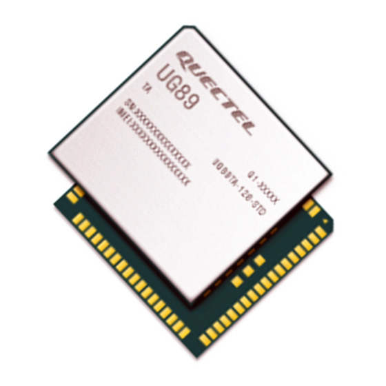
Page 60: Top And Bottom Views Of The Module
UMTS/HSPA+ Module Series UG89 Hardware Design 6.3. Top and Bottom Views of the Module Figure 32: Top View of the Module Figure 33: Bottom View of the Module UG89_Hardware_Design 59 / 73... - Page 61 UMTS/HSPA+ Module Series UG89 Hardware Design NOTE These are renderings of UG89 module. For authentic dimension and appearance, please refer to the module that you receive from Quectel. UG89_Hardware_Design 60 / 73...
-
Page 62: Storage, Manufacturing And Packaging
Storage, Manufacturing and Packaging 7.1. Storage UG89 is stored in the vacuum-sealed bag. It is rated at MSL 3 and its storage restrictions are shown as below. Shelf life in the vacuum-sealed bag: 12 months at <40º C/<90%RH. After the vacuum-sealed bag is opened, devices that will be subjected to reflow soldering or other high temperature processes must be: ... -
Page 63: Manufacturing And Soldering
UMTS/HSPA+ Module Series UG89 Hardware Design 7.2. Manufacturing and Soldering Push the squeegee to apply the solder paste on the surface of stencil, thus making the paste fill the stencil openings and then penetrate to the PCB. The force on the squeegee should be adjusted properly so as to produce a clean stencil surface on a single pass. -
Page 64: Packaging
2D barcode is still readable, although white rust may be found. 7.3. Packaging UG89 is packaged in a vacuum-sealed bag which is ESD protected. The bag should not be opened until the devices are ready to be soldered onto the application. -
Page 65: Appendix A References
Appendix A References Table 32: Related Documents Document Name Remark Quectel_Module_Secondary_SMT_User_Guide Module Secondary SMT User Guide Quectel_UG89_AT_Commands_Manual UG89 AT Commands Manual Quectel_RF_Layout_Application_Note RF Layout Application Note UMTS<E EVB user guide for UMTS<E Quectel_UMTS<E_EVB_User_Guide modules Table 33: Terms and Abbreviations Abbreviation... - Page 66 UMTS/HSPA+ Module Series UG89 Hardware Design Electrostatic Discharge Equivalent Series Resistance Frequency Division Duplex Full Rate File Transfer Protocol FTPS FTP-over-SSL GMSK Gaussian Minimum Shift Keying Global System for Mobile Communications Half Rate HSPA High Speed Packet Access HSDPA High Speed Downlink Packet Access...
- Page 67 UMTS/HSPA+ Module Series UG89 Hardware Design Point-to-Point Protocol Phase Shift Keying Quadrature Amplitude Modulation QPSK Quadrature Phase Shift Keying Radio Frequency Short Message Service SMTP Simple Mail Transfer Protocol Secure Sockets Layer Transmission Control Protocol Time Division Duplexing UART Universal Asynchronous Receiver &Transmitter...
- Page 68 UMTS/HSPA+ Module Series UG89 Hardware Design Maximum Output Low Level Voltage Value Minimum Output Low Level Voltage Value VSWR Voltage Standing Wave Ratio WCDMA Wideband Code Division Multiple Access WLAN Wireless Local Area Network UG89_Hardware_Design 67 / 73...
-
Page 69: Appendix B Gprs Coding Schemes
UMTS/HSPA+ Module Series UG89 Hardware Design Appendix B GPRS Coding Schemes Table 34: Description of Different Coding Schemes Scheme CS-1 CS-2 CS-3 CS-4 Code Rate Pre-coded USF Radio Block excl.USF and BCS Tail Coded Bits Punctured Bits Data Rate Kb/s 9.05... -
Page 70: Appendix C Gprs Multi-Slot Classes
UMTS/HSPA+ Module Series UG89 Hardware Design Appendix C GPRS Multi-slot Classes Twenty-nine classes of GPRS multi-slot modes are defined for MS in GPRS specification. Multi-slot classes are product dependent, and determine the maximum achievable data rates in both the uplink and downlink directions. - Page 71 UMTS/HSPA+ Module Series UG89 Hardware Design UG89_Hardware_Design 70 / 73...
-
Page 72: Appendix D Edge Modulation And Coding Schemes
UMTS/HSPA+ Module Series UG89 Hardware Design Appendix D EDGE Modulation and Coding Schemes Table 36: EDGE Modulation and Coding Schemes Coding Scheme Modulation Coding Family 1 Timeslot 2 Timeslot 4 Timeslot CS-1: GMSK 9.05kbps 18.1kbps 36.2kbps CS-2: GMSK 13.4kbps 26.8kbps 53.6kbps... -
Page 73: Appendix E Certification List
UMTS/HSPA+ Module Series UG89 Hardware Design Appendix E Certification List Table 37: Certification List Country or Operator Comment Certification Australia Government RCM 2 months Australia Telstra 4 months(need RCM & GCF) Australia Vodafone 3 months(need FCC & PTCRB) Brazil Government ANATEL... - Page 74 UMTS/HSPA+ Module Series UG89 Hardware Design UK Vodafone 3 months(need CE & GCF) FCC/IC: 2 months USA FCC/IC/PTCRB/UL Gov. PTCRB: 3 months UL: Modules do not need to do UL. USA AT&T 5~6 Months(need FCC & PTCRB). UG89_Hardware_Design 73 / 73...
- Page 75 FCC KDB996369 D03v01 Requirements List of applicable FCC rules FCC Part 15 Subpart B, Part 22 Subpart H, Part 24 Subpart E Summarize the specific operational use conditions Not Applicable Limited module procedures Not Applicable Trace antenna designs Refer to Manual Section 4 RF exposure considerations Refer to FCC certification requirements Antennas...
- Page 76 FCC Certification Requirements. According to the definition of mobile and fixed device is described in Part 2.1091(b), this device is a mobile device. And the following conditions must be met: 1. This Modular Approval is limited to OEM installation for mobile and fixed applications only. The antenna installation and operating configurations of this transmitter, including any applicable source-based time-averaging duty factor, antenna gain and cable loss must satisfy MPE categorical Exclusion Requirements of 2.1091.
- Page 77 provided the user can reasonably be expected to have the capability to access information in that form. This device complies with part 15 of the FCC Rules. Operation is subject to the following two conditions: (1) This device may not cause harmful interference, and (2) this device must accept any interference received, including interference that may cause undesired operation.
- Page 78 Antennas Technology Frequency Range Antenna Type Max Peak Gain (dBi) (MHz) GSM850 824.2 ~ 848.8 2.29 PCS1900 1850.2 ~ 1909.8 1.59 Dipole WCDMA Band II 1852.4 ~ 1907.6 1.59 WCDMA Band V 826.4 ~ 846.6 2.29 Antennes Technologie Gamme de Type d'antenne Gain de crête fréquences (MHz)
Need help?
Do you have a question about the UG89 and is the answer not in the manual?
Questions and answers