Table of Contents
Advertisement
Quick Links
Features
•
High-performance, Low-power AVR
•
Advanced RISC Architecture
– 90 Powerful Instructions – Most Single-clock Cycle Execution
– 32 x 8 General-purpose Working Registers
– Fully Static Operation
•
Nonvolatile Program and Data Memories
– 1K bytes In-System Programmable Flash Program Memory
Endurance: 1,000 Write/Erase Cycles
– 64 bytes EEPROM
Endurance: 100,000 Write/Erase Cycles
– Programming Lock for Flash Program Data Security
•
Peripheral Features
– Interrupt and Wakeup on Pin Change
– Two 8-bit Timer/Counters with Separate Prescalers
– One150 kHz, 8-bit High-speed PWM Output
– 4 channel 10-bit ADC
One Differential Voltage Input with Optional Gain of 20x
– On-chip Analog Comparator
– Programmable Watchdog Timer with On-chip Oscillator
•
Special Microcontroller Features
– In-System Programmable via SPI Port
– Enhanced Power-on Reset Circuit
– Programmable Brown-out Detection Circuit
– Internal, Calibrated 1.6 MHz Tuneable Oscillator
– Internal 25.6 MHz Clock Generator for Timer/Counter
– External and Internal Interrupt Sources
– Low-power Idle and Power-down Modes
•
I/O and Packages
– 8-pin PDIP/SOIC: 6 Programmable I/O Lines
•
Operating Voltages
– 2.7V - 5.5V (ATtiny15L)
•
Internal 1.6 MHz System Clock
•
Commercial and Industrial Temperature Ranges
Description
The ATtiny15L is a low-power CMOS 8-bit microcontroller based on the AVR RISC
architecture. By executing powerful instructions in a single-clock cycle, the ATtiny15L
achieves throughputs approaching 1 MIPS per MHz allowing the system designer to
optimize power consumption versus processing speed.
Pin Configuration
PDIP/SOIC
(RESET/ADC0) PB5
1
(ADC3) PB4
2
(ADC2) PB3
3
GND
4
®
8-bit Microcontroller
8
VCC
7
PB2 (ADC1/SCK/T0/INT0)
6
PB1 (AIN1/MISO/OC1A)
5
PB0 (AIN0/AREF/MOSI)
8-bit
Microcontroller
with 1K Bytes
Flash
ATtiny15L
Advance
Information
(continued)
Rev. 1187B–03/00
1
Advertisement
Table of Contents

Related Manuals for Atmel AVR ATtiny15L


Summary of Contents for Atmel AVR ATtiny15L
- Page 1 Features ® • High-performance, Low-power AVR 8-bit Microcontroller • Advanced RISC Architecture – 90 Powerful Instructions – Most Single-clock Cycle Execution – 32 x 8 General-purpose Working Registers – Fully Static Operation • Nonvolatile Program and Data Memories – 1K bytes In-System Programmable Flash Program Memory Endurance: 1,000 Write/Erase Cycles –...
- Page 2 The device is manufactured using Atmel’s high density nonvolatile memory technology. By combining an enhanced RISC 8-bit CPU with Flash on a monolithic chip, the Atmel ATtiny15L is a powerful microcontroller that provides a highly-flexible and cost-efficient solution to many embedded control applications. The peripheral features make the ATtiny15L particularly suited for battery chargers, lighting ballasts, and all kinds of intelligent sensor applications.
-
Page 3: Block Diagram
ATtiny15L Block Diagram Figure 1. The ATtiny15L Block Diagram 8-BIT DATABUS TUNABLE INTERNAL INTERNAL OSCILLATOR OSCILLATOR PROGRAM STACK WATCHDOG TIMING AND POINTER TIMER CONTROL COUNTER MCU CONTROL PROGRAM HARDWARE REGISTER FLASH STACK INSTRUCTION MCU STATUS REGISTER REGISTER GENERAL PURPOSE REGISTERS INSTRUCTION TIMER/ DECODER... -
Page 4: Pin Descriptions
Pin Descriptions Supply voltage pin. Ground pin. Port B (PB5..PB0) Port B is a 6-bit I/O port. PB4..0 are I/O pins that can provide internal pull-ups (selected for each bit). PB5 is input or open- drain output. The use of pin PB5 is defined by a fuse and the special function associated with this pin is external Reset. The port pins are tri-stated when a reset condition becomes active, even if the clock is not running. -
Page 5: Attiny15L Architectural Overview
ATtiny15L ATtiny15L Architectural Overview The fast-access register file concept contains 32 x 8-bit general-purpose working registers with a single-clock-cycle access time. This means that during one single-clock cycle, one ALU (Arithmetic Logic Unit) operation is executed. Two operands are output from the register file, the operation is executed, and the result is stored back in the register file – in one clock cycle. - Page 6 The General-purpose Register File Figure 3 shows the structure of the 32 general-purpose registers in the CPU. Figure 3. AVR CPU General-purpose Working Registers General … Purpose … Working Registers R30 (Z-Register low byte)R3 R31 (Z-Register high byte) All the register operating instructions in the instruction set have direct- and single-cycle access to all registers. The only exception is the five constant arithmetic and logic instructions SBCI, SUBI, CPI, ANDI, and ORI between a constant and a register and the LDI instruction for load-immediate constant data.
- Page 7 ATtiny15L Register Direct, Single-register Rd Figure 4. Direct Single-register Addressing The operand is contained in register d (Rd). Register Indirect Figure 5. Indirect Register Addressing The register accessed is the one pointed to by the Z-register low byte (R30). Register Direct, Two Registers Rd and Rr Figure 6.
- Page 8 I/O Direct Figure 7. I/O Direct Addressing Operand address is contained in 6 bits of the instruction word. n is the destination or source register address. Relative Program Addressing, RJMP and RCALL Figure 8. Relative Program Memory Addressing Program execution continues at address PC + k + 1. The relative address k is -2048 to 2047. Constant Addressing Using the LPM Instruction Figure 9.
-
Page 9: Subroutine And Interrupt Hardware Stack
ATtiny15L Subroutine and Interrupt Hardware Stack The ATtiny15L uses a 3-level deep hardware stack for subroutines and interrupts. The hardware stack is 9-bit wide and stores the Program Counter (PC) return address while subroutines and interrupts are executed. RCALL instructions and interrupts push the PC return address onto stack level 0, and the data in the other stack levels 1-2 are pushed one level deeper in the stack. - Page 10 I/O Memory The I/O space definition of the ATtiny15L is shown in the following table: Table 2. ATtiny15L I/O Space Address Hex Name Function SREG Status Register GIMSK General Interrupt Mask Register GIFR General Interrupt Flag Register TIMSK Timer/Counter Interrupt Mask Register TIFR Timer/Counter Interrupt Flag Register MCUCR...
-
Page 11: Reset And Interrupt Handling
ATtiny15L The Status Register – SREG The AVR status register – SREG – at I/O space location $3F is defined as: SREG Read/Write Initial value • Bit 7 - I: Global Interrupt Enable The global interrupt enable bit must be set (one) for the interrupts to be enabled. The individual interrupt enable control is then performed in the interrupt mask registers –... - Page 12 Table 3. Reset and Interrupt Vectors Vector No. Program Address Source Interrupt Definition External Reset, Power-on Reset, Brown-out Reset, $000 RESET and Watchdog Reset $001 INT0 External Interrupt Request 0 $002 I/O Pins Pin Change Interrupt $003 TIMER1, COMPA Timer/Counter1 Compare Match A $004 TIMER1, OVF Timer/Counter1 Overflow...
-
Page 13: Attiny15L Reset Sources
ATtiny15L ATtiny15L Reset Sources The ATtiny15L has four sources of reset: • Power-on Reset. The MCU is reset when the supply voltage is below the power-on reset threshold (V • External Reset. The MCU is reset when a low-level is present on the RESET pin for more than 500 ns. •... - Page 14 Table 4. Reset Characteristics (V = 5.0V) Symbol Parameter Condition Units Power-on Reset Threshold Voltage (rising) BOD disabled BOD enabled Power-on Reset Threshold Voltage (falling) BOD disabled BOD enabled RESET Pin Threshold Voltage 0.85V Brown-out Reset Threshold Voltage (BODLEVEL = 1) (BODLEVEL = 0) Note: 1.
- Page 15 ATtiny15L Power-on Reset A power-on reset (POR) pulse is generated by an on-chip detection circuit. The detection level is nominally defined in Table 4. The POR is activated whenever V is below the detection level. The POR circuit can be used to trigger the start-up reset, as well as detect a failure in supply voltage.
- Page 16 External Reset An external reset is generated by a low-level on the RESET pin. Reset pulses longer than 500 ns will generate a reset, even if the clock is not running. Shorter pulses are not guaranteed to generate a reset. When the applied signal reaches the Reset Threshold Voltage –...
- Page 17 ATtiny15L Watchdog Reset When the Watchdog times out, it will generate a short reset pulse of 1 CK cycle duration. On the falling edge of this pulse, the delay timer starts counting the Time-out period t . Refer to page 32 for details on operation of the Watchdog Timer. TOUT Figure 17.
-
Page 18: Internal Voltage Reference
Internal Voltage Reference ATtiny15L features an internal bandgap reference with a nominal voltage of 1.22V. This reference is used for Brown-out Detection, and it can be used as an input to the Analog Comparator. The 2.56V reference to the ADC is generated from the internal bandgap reference. - Page 19 ATtiny15L The General Interrupt Mask Register – GIMSK INT0 PCIE GIMSK Read/Write Initial value • Bit 7 - Res: Reserved Bit This bit is a reserved bit in the ATtiny15L and always reads as zero. • Bit 6 - INT0: External Interrupt Request 0 Enable When the INT0 bit is set (one) and the I-bit in the Status Register (SREG) is set (one), the external pin interrupt is activated.
- Page 20 The Timer/Counter Interrupt Mask Register – TIMSK OCIE1A TOIE1 TOIE0 TIMSK Read/Write Initial value • Bit 7 - Res: Reserved bit This bit is a reserved bit in the ATtiny15L and always reads as zero. • Bit 6 - OCIE1A: Timer/Counter1 Output Compare Interrupt Enable When the OCIE1A bit is set (one)and the I-bit in the Status Register is set (one), the Timer/Counter1 Compare Match, inter- rupt is enabled.
- Page 21 ATtiny15L External Interrupt The external interrupt is triggered by the INT0 pin. Observe that, if enabled, the interrupt will trigger even if the INT0 pin is configured as an output. This feature provides a way of generating a software interrupt. The external interrupt can be trig- gered by a falling or rising edge, a pin change, or a low-level.
-
Page 22: Sleep Modes
• Bits 1, 0 - ISC01, ISC00: Interrupt Sense Control 0 bit 1 and bit 0 The External Interrupt 0 is activated by the external pin INT0 if the SREG I-flag and the corresponding interrupt mask is set (one). The activity on the external INT0 pin that activates the interrupt is defined in the following table: Table 8. -
Page 23: Internal Pll For Fast Peripheral Clock Generation
ATtiny15L Tunable Internal RC Oscillator The internal RC oscillator provides a fixed 1.6 MHz clock (nominal at 5V and 25 ° C). This internal clock is always the system clock of the ATtiny15L. This oscillator can be calibrated by writing the calibration byte (see page 48) to the OSCCAL register. -
Page 24: The Timer/Counter0 Prescaler
Timer/Counters The ATtiny15L provides two general-purpose 8-bit Timer/Counters. The Timer/Counters have separate prescaling selec- tion from separate 10-bit prescalers. The Timer/Counter0 uses internal clock (CK) as the clock timebase. The Timer/Counter1 may use either the internal clock (CK) or the fast peripheral clock (PCK) as the clock time base. The Timer/Counter0 Prescaler Figure below shows the Timer/Counter prescaler. -
Page 25: The Special Function Io Register - Sfior
ATtiny15L Figure 19. Timer/Counter1 Prescaler 10-BIT T/C PRESCALER (1.6 MHz) CLEAR PSR1 CLEAR 3-BIT T/C PRESCALER (25.6 MHz) CS10 CS11 CS12 CS13 TIMER/COUNTER1 CLOCK SOURCE The Special Function IO Register – SFIOR FOC1A PSR1 PSR0 SFIOR Read/Write Initial value • Bit 7...3 - Res: Reserved Bits These bits are reserved bits in the ATtiny15L and always read as zero. - Page 26 The 8-bit Timer/Counter0 features both a high-resolution and a high-accuracy usage with the lower prescaling opportuni- ties. Similarly, the high-prescaling opportunities make the Timer/Counter0 useful for lower-speed functions or exact-timing functions with infrequent actions. Figure 20. Timer/Counter0 Block Diagram T/C CLK SOURCE The Timer/Counter0 Control Register –...
-
Page 27: The Timer Counter 0 - Tcnt0
ATtiny15L The Timer Counter 0 – TCNT0 TCNT0 Read/Write Initial value The Timer/Counter0 is implemented as an up-counter with read and write access. If the Timer/Counter0 is written and a clock source is present, the Timer/Counter0 continues counting in the timer clock cycle following the write operation. The 8-bit Timer/Counter1 This module features a high-resolution and a high-accuracy usage with the lower prescaling opportunities. - Page 28 The Timer/Counter1 contains two Output Compare registers, OCR1A and OCR1B as the data source to be compared with the Timer/Counter1 contents. In normal mode the Output Compare function is operational with OCR1A only, and the Out- put Compare function includes optional clearing of the counter on compare match, and action on the Output Compare Pin –...
- Page 29 ATtiny15L • Bits 3,2,1,0 - CS13, CS12, CS11, CS10: Clock Select bits 3, 2, 1, and 0 The Clock Select bits 3, 2, 1, and 0 define the prescaling source of Timer/Counter1. Table 11. Timer/Counter1 Prescale Select CS13 CS12 CS11 CS10 Description Timer/Counter1 is stopped.
- Page 30 Timer/Counter1 in PWM mode When the PWM mode is selected, Timer/Counter1 and the Output Compare Register A – OCR1A form an 8-bit, free-run- ning and glitch-free PWM with outputs on the PB1(OC1A) pin. Timer/Counter1 acts as an up-counter, counting up from $00 up to the value specified in the second output compare register OCR1B, and starting from $00 up again.
- Page 31 ATtiny15L Timer/Counter1 Output Compare RegisterB – OCR1B OCR1B Read/Write Initial value The output compare register1 OCR1B is an 8-bit read/write register. This register is used in the PWM mode only, and it lim- its the top value to which the Timer/Counter1 keeps counting. After reaching OCR1B in PWM mode, the counter starts from $00.
-
Page 32: The Watchdog Timer
The Watchdog Timer The Watchdog Timer is clocked from a separate on-chip oscillator which runs at 1 MHz. This is the typical value at V 5V. See characterization data for typical values at other V levels. By controlling the Watchdog Timer prescaler, the Watchdog reset interval can be adjusted from 16 to 2048 ms as shown in Table 15. -
Page 33: Eeprom Read/Write Access
ATtiny15L Table 15. Watch Dog Timer Prescale Select WDP2 WDP1 WDP0 Time-out Period 16K cycles 32K cycles 64K cycles 128K cycles 256K cycles 512K cycles 1024K cycles 2048K cycles EEPROM Read/Write Access The EEPROM access registers are accessible in the I/O space. The write access time is in the range of 1.1 - 2.1 ms, depending on the V voltages. - Page 34 The EEPROM Data Register – EEDR EEDR Read/Write Initial value • Bit 7..0 - EEDR7..0: EEPROM Data For the EEPROM write operation, the EEDR register contains the data to be written to the EEPROM in the address given by the EEAR register. For the EEPROM read operation, the EEDR contains the data read out from the EEPROM at the address given by EEAR.
-
Page 35: Preventing Eeprom Corruption
ATtiny15L Preventing EEPROM Corruption During periods of low V the EEPROM data can be corrupted because the supply voltage is too low for the CPU and the EEPROM to operate properly. These issues are the same as for board-level systems using the EEPROM, and the same design solutions should be applied. - Page 36 The Analog Comparator Control And Status Register – ACSR ACBG ACIE ACIS1 ACIS0 ACSR Read/Write Initial value • Bit 7 - ACD: Analog Comparator Disable When this bit is set(one), the power to the analog comparator is switched off. This bit can be set at any time to turn-off the analog comparator.
-
Page 37: The Analog To Digital Converter, Analog Multiplexer And Gain Stages
ATtiny15L The Analog to Digital Converter, Analog Multiplexer and Gain Stages Feature list: • 10-bit Resolution • ±2 LSB Absolute Accuracy • 0.5 LSB Integral Non-linearity • Optional Offset Cancellation • 65 - 260 µs Conversion Time • Up to 15 kSPS •... -
Page 38: Operation
Figure 25. Analog to Digital Converter Block Schematic ADC CONVERSION COMPLETE IRQ 8-BIT DATA BUS ADC DATA REGISTER ADC MULTIPLEXER ADC CTRL. & STATUS (ADCH/ADCL) SELECT (ADMUX) REGISTER (ADCSR) PRESCALER MUX DECODER CONVERSION LOGIC AREF SAMPLE & HOLD COMPARATOR INTERNAL 2.56 V 10-BIT DAC REFERENCE... -
Page 39: Prescaling And Conversion Timing
ATtiny15L The ADC is enabled by setting the ADC Enable bit, ADEN in ADCSR. Voltage reference and input channel selections will not go into effect until ADEN is set. The ADC does not consume power when ADEN is cleared, so it is recommended to switch off the ADC before entering power-saving sleep modes. - Page 40 The actual sample-and-hold takes place 1.5 ADC clock cycles after the start of a normal conversion and 13.5 ADC clock cycles after the start of an extended conversion. When a conversion is complete, the result is written to the ADC data reg- isters, and ADIF is set.
-
Page 41: Adc Noise Canceler Function
ATtiny15L Figure 29. ADC Timing Diagram, Free Running Conversion One Conversion Next Conversion Cycle number ADC clock ADSC ADIF ADCH Sign and MSB of result ADCL LSB of result Sample & hold Conversion complete MUX and REFS update Table 17. ADC Conversion Time Sample &... - Page 42 The ADC Multiplexer Selection Register – ADMUX REFS1 REFS0 ADLAR MUX2 MUX1 MUX0 ADMUX Read/Write Initial value • Bits 7..6 - REFS1..REFS0: Reference Selection Bits These bits select the voltage reference for the ADC, as shown in Table 18. If these bits are changed during a conversion, the change will not go in effect until this conversion is complete (ADIF in ADCSR is set).
- Page 43 ATtiny15L The ADC Control and Status Register – ADCSR ADEN ADSC ADFR ADIF ADIE ADPS2 ADPS1 ADPS0 ADCSR Read/Write Initial value • Bit 7 - ADEN: ADC Enable Writing a logical “1” to this bit enables the ADC. By clearing this bit to zero, the ADC is turned off. Turning the ADC off while a conversion is in progress, will terminate this conversion.
-
Page 44: Adc Noise Canceling Techniques
The ADC Data Register - ADCL and ADCH ADLAR = 0: ADC9 ADC8 ADCH ADC7 ADC6 ADC5 ADC4 ADC3 ADC2 ADC1 ADC0 ADCL Read/Write Initial value ADLAR = 1: ADC9 ADC8 ADC7 ADC6 ADC5 ADC4 ADC3 ADC2 ADCH ADC1 ADC0 ADCL Read/Write Initial value... -
Page 45: Adc Characteristics
ATtiny15L ADC Characteristics Symbol Parameter Condition Units Resolution Single Ended Conversion Bits Differential Conversion Gain = 1x or 20x Bits Absolute accuracy Single Ended Conversion = 4V ADC clock = 200 kHz Single Ended Conversion = 4V ADC clock = 1 MHz Single Ended Conversion = 4V ADC clock = 2 MHz... - Page 46 I/O Port B All AVR ports have true Read-modify-write functionality when used as general digital I/O ports. This means that the direc- tion of one port pin can be changed without unintentionally changing the direction of any other pin with the SBI and CBI instructions.
- Page 47 ATtiny15L PORT B as General Digital I/O The lower 5 pins in port B are equal when used as digital I/O pins. PBn, General I/O pin: The DDBn bit in the DDRB register selects the direction of this pin, if DDBn is set (one), PBn is con- figured as an output pin.
-
Page 48: Memory Programming
Power-on Reset. If not, the part can fail to enter programming mode caused by drive contention on PB0 and/or PB5. Signature Bytes All Atmel microcontrollers have a three-byte signature code which identifies the device. The three bytes resides in a separate address space, and for the ATtiny15L they are: 1. -
Page 49: Programming The Flash
ATtiny15L Programming the Flash Atmel’s ATtiny15L offers 1K bytes of in-system reprogrammable Flash Program memory and 64 bytes of in-system repro- grammable EEPROM data memory. The ATtiny15L is shipped with the on-chip Flash Program and EEPROM Data memory arrays in the erased state (i.e. con- tents = $FF) and ready to be programmed. -
Page 50: High-Voltage Serial Programming Algorithm
High-voltage Serial Programming Algorithm To program and verify the ATtiny15L in the high-voltage serial programming mode, the following sequence is recom- mended (See instruction formats in Table 24): 1. Power-up sequence: Apply 4.5 - 5.5V between VCC and GND. Set PB5 and PB0 to “0” and wait at least 30 µs. Set PB3 to “0”. - Page 51 ATtiny15L Table 24. High-voltage Serial Programming Instruction Set for ATtiny15L Instruction Format Instruction Instr.1 Instr.2 Instr.3 Instr.4 Operation Remarks Chip Erase 0_1000_0000_00 0_0000_0000_00 0_0000_0000_00 0_0000_0000_00 Wait after Instr.3 until PB2 goes high for the Chip Erase cycle to 0_0100_1100_00 0_0110_0100_00 0_0110_1100_00 0_0100_1100_00 finish.
- Page 52 Table 24. High-voltage Serial Programming Instruction Set for ATtiny15L (Continued) Instruction Format Instruction Instr.1 Instr.2 Instr.3 Instr.4 Operation Remarks Read Lock bits 0_0000_0100_00 0_0000_0000_00 0_0000_0000_00 Reading 2, 1 = “0” means the Lock bit is programmed 0_0100_1100_00 0_0111_1000_00 0_0111_1100_00 x_xxxx_xxxx_xx x_xxxx_xxxx_xx x_xxxx_21xx_xx Read Signature...
-
Page 53: High-Voltage Serial Programming Characteristics
ATtiny15L High-voltage Serial Programming Characteristics Figure 32. High-voltage Serial Programming Timing SDI (PB0), SII (PB1) VALID IVSH SHIX SHSL SLSH SCI (PB3) SDO (PB2) SHOV Internal CK Table 25. High-voltage Serial Programming Characteristics = 25 ° C ± 10%, V = 5.0V ±... - Page 54 Low-voltage Serial Programming Algorithm When writing serial data to the ATtiny15L, data is clocked on the rising edge of SCK. When reading data from the ATtiny15L, data is clocked on the falling edge of SCK. See Figure 34, Figure 35 and Table 27 for timing details. To program and verify the ATtiny15L in the serial programming mode, the following sequence is recommended (See four byte instruc- tion formats in Table 26 ): 1.
- Page 55 ATtiny15L Table 26. Low-voltage Serial Programming Instruction Set Instruction Instruction Format Operation Byte 1 Byte 2 Byte 3 Byte4 Enable Serial Programming while 1010 1100 0101 0011 xxxx xxxx xxxx xxxx Programming Enable RESET is low. Chip Erase Flash and EEPROM 1010 1100 100x xxxx xxxx xxxx...
-
Page 56: Low-Voltage Serial Programming Characteristics
Low-voltage Serial Programming Characteristics Figure 35. Low-voltage Serial Programming Timing MOSI SLSH OVSH SHOX SHSL MISO SLIV Table 27. Low-voltage Serial Programming Characteristics = -40 ° C to 85 ° C, V = 2.7 - 5.5V (Unless otherwise noted) Symbol Parameter Units RC Oscillator Frequency (V... - Page 57 ATtiny15L DC Characteristics – Preliminary Data = -40 ° C to 85 ° C, V = 2.7V to 5.5V Symbol Parameter Condition Units Input Low Voltage Except (XTAL) -0.5 0.3 V Input Low Voltage XTAL -0.5 0.1 V Input High Voltage Except (XTAL, RESET) 0.6 V + 0.5...
- Page 58 Typical characteristics – PRELIMINARY DATA The following charts show typical behavior. These data are characterized, but not tested. All current consumption measure- ments are performed with all I/O pins configured as inputs and with internal pull-ups enabled. The current consumption is a function of several factors such as: operating voltage, operating frequency, loading of I/O pins, switching rate of I/O pins, code executed, and ambient temperature.
- Page 59 ATtiny15L Figure 37. Analog Comparator Offset Voltage vs. Common Mode Voltage ANALOG COMPARATOR OFFSET VOLTAGE vs. COMMON MODE VOLTAGE V = 5V T = 25 ˚ T = 85 ˚ Common Mode Voltage (V) Analog comparator offset voltage is measured as absolute offset Figure 38.
- Page 60 Figure 39. Analog Comparator Input Leakage Current ANALOG COMPARATOR INPUT LEAKAGE CURRENT V = 6V T = 25 ˚ V (V) Figure 40. Watchdog Oscillator Frequency vs. V WATCHDOG OSCILLATOR FREQUENCY vs. V 1600 1400 T = 25 ˚ 1200 T = 85 ˚...
- Page 61 ATtiny15L Figure 41. Pull-up Resistor Current vs. Input Voltage PULL-UP RESISTOR CURRENT vs. INPUT VOLTAGE V = 5V T = 25 ˚ T = 85 ˚ Figure 42. Pull-up Resistor Current vs. Input Voltage PULL-UP RESISTOR CURRENT vs. INPUT VOLTAGE V = 2.7V T = 25 ˚...
- Page 62 Figure 43. I/O Pin Sink Current vs. Output Voltage I/O PIN SINK CURRENT vs. OUTPUT VOLTAGE V = 5V T = 25 ˚ T = 85 ˚ Figure 44. I/O Pin Source Current vs. Output Voltage I/O PIN SOURCE CURRENT vs. OUTPUT VOLTAGE V = 5V T = 25 ˚...
- Page 63 ATtiny15L Figure 45. I/O Pin Sink Current vs. Output Voltage I/O PIN SINK CURRENT vs. OUTPUT VOLTAGE V = 2.7V T = 25 ˚ T = 85 ˚ Figure 46. I/O Pin Source Current vs. Output Voltage I/O PIN SOURCE CURRENT vs. OUTPUT VOLTAGE V = 2.7V T = 25 ˚...
- Page 64 Figure 47. I/O Pin Input Threshold Voltage vs. V I/O PIN INPUT THRESHOLD VOLTAGE vs. V T = 25 ˚ Figure 48. I/O Pin Input Hysteresis vs. V I/O PIN INPUT HYSTERESIS vs. V T = 25 ˚ 0.18 0.16 0.14 0.12 0.08...
-
Page 65: Attiny15L Register Summary
ATtiny15L ATtiny15L Register Summary Address Name Bit 7 Bit 6 Bit 5 Bit 4 Bit 3 Bit 2 Bit 1 Bit 0 Page SREG Reserved Reserved GIMSK INT0 PCIE GIFR INTF0 PCIF TIMSK OCIE1A TOIE1 TOIE0 TIFR OCF1A TOV1 TOV0 Reserved Reserved MCUCR... -
Page 66: Attiny15L Instruction Set Summary
ATtiny15L Instruction Set Summary Mnemonics Operands Description Operation Flags #Clocks ARITHMETIC AND LOGIC INSTRUCTIONS Rd, Rr Add two Registers Rd + Rr Z,C,N,V,H ← Rd, Rr Add with Carry two Registers Rd + Rr + C Z,C,N,V,H ← Rd, Rr Subtract two Registers Rd - Rr Z,C,N,V,H... - Page 67 ATtiny15L ATtiny15L Instruction Set Summary (Continued) Mnemonics Operands Description Operation Flags #Clocks DATA TRANSFER INSTRUCTIONS Rd, Z Load Register Indirect None ← Z, Rr Store Register Indirect None ← Rd, Rr Move Between Registers None ← Rd, K Load Immediate None =←...
-
Page 68: Ordering Information
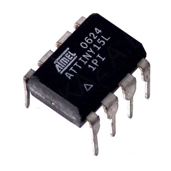
Ordering Information Power Supply Speed (MHz) Ordering Code Package Operation Range 2.7 - 5.5V ATtiny15L-1PC Commercial ATtiny15L-1SC (0°C to 70°C) ATtiny15L-1PI Industrial ATtiny15L-1SI (-40°C to 85°C) Package Type 8-lead, 0.300" Wide, Plastic Dual Inline Package (PDIP) 8-lead, 0.200" Wide, Plastic Gull Wing Small Outline (EIAJ SOIC) ATtiny15L... -
Page 69: Packaging Information
ATtiny15L Packaging Information 8P3, 8-lead, 0.300" Wide, Plastic Dual Inline 8S2, 8-lead, 0.210" Wide, Plastic Gull Wing Small Package (PDIP) Outline (EIAJ SOIC) Dimensions in Inches and (Millimeters) Dimensions in Inches and (Millimeters) .400 (10.16) .020 (.508) .355 (9.02) .012 (.305) .213 (5.41) .330 (8.38) .280 (7.11) - Page 70 No licenses to patents or other intellectual prop- erty of Atmel are granted by the Company in connection with the sale of Atmel products, expressly or by implication. Atmel’s products are not authorized for use as critical components in life suppor t devices or systems.
Need help?
Do you have a question about the AVR ATtiny15L and is the answer not in the manual?
Questions and answers