Table of Contents
Advertisement
Quick Links
Features
®
•
Utilizes the AVR
RISC Architecture
•
AVR - High-performance and Low-power RISC Architecture
– 118 Powerful Instructions - Most Single Clock Cycle Execution
– 32 x 8 General Purpose Working Registers
– Up to 8 MIPS Throughput at 8 MHz
•
Data and Nonvolatile Program Memory
– 2K Bytes of In-System Programmable Flash
Endurance 1,000 Write/Erase Cycles
– 128 Bytes of internal SRAM
– 128 Bytes of In-System Programmable EEPROM
Endurance: 100,000 Write/Erase Cycles
– Programming Lock for Flash Program and EEPROM Data Security
•
Peripheral Features
– One 8-bit Timer/Counter with Separate Prescaler
– Programmable Watchdog Timer with On-chip Oscillator
– SPI Serial Interface for In-System Programming
•
Special Microcontroller Features
– Low-power Idle and Power Down Modes
– External and Internal Interrupt Sources
– Power-on Reset Circuit
– Selectable On-chip RC Oscillator
•
Specifications
– Low-power, High-speed CMOS Process Technology
– Fully Static Operation
•
Power Consumption at 4 MHz, 3V, 25°C
– Active: 2.4 mA
– Idle Mode: 0.5 mA
– Power Down Mode: <1 µA
•
I/O and Packages
– 5 Programmable I/O Lines
– 8-pin PDIP and SOIC
•
Operating Voltages
– 2.7 - 6.0V (ATtiny22L)
– 4.0 - 6.0V (ATtiny22)
•
Speed Grades
– 0 - 4 MHz (ATtiny22L)
– 0 - 8 MHz (ATtiny22)
Description
The ATtiny22/L is a low-power CMOS 8-bit microcontrollers based on the AVR RISC
architecture. By executing powerful instructions in a single clock cycle, the ATtiny22/L
achieves throughputs approaching 1 MIPS per MHz allowing the system designer to
optimize power consumption versus processing speed.
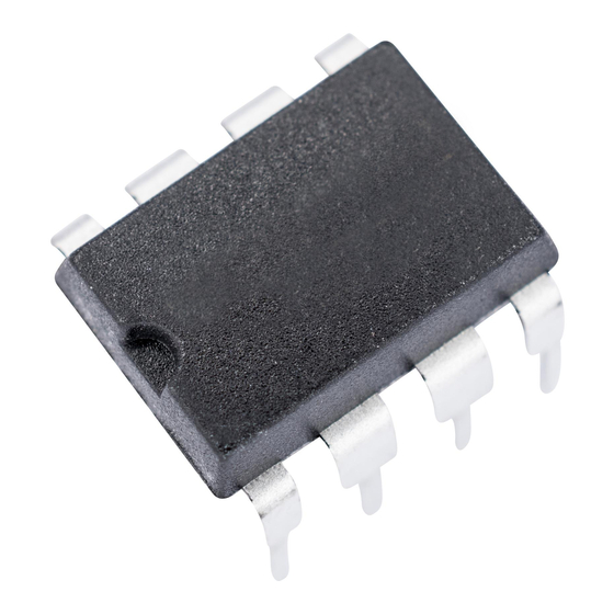
Pin Configuration
(CLOCK) PB3
PDIP/SOIC
RESET
1
8
VCC
2
7
PB2 (SCK/T0)
PB4
3
6
PB1 (MISO/INT0)
GND
4
5
PB0 (MOSI)
8-bit
Microcontroller
with 2K Bytes of
In-System
Programmable
Flash
ATtiny22
ATtiny22L
Preliminary
Rev. 1273A–04/99
1
Advertisement
Table of Contents

Related Manuals for Atmel AVR ATtiny22


Summary of Contents for Atmel AVR ATtiny22
- Page 1 Features ® • Utilizes the AVR RISC Architecture • AVR - High-performance and Low-power RISC Architecture – 118 Powerful Instructions - Most Single Clock Cycle Execution – 32 x 8 General Purpose Working Registers – Up to 8 MIPS Throughput at 8 MHz •...
-
Page 2: Block Diagram
The AVR core combines a rich instruction set with 32 general purpose working registers. All the 32 registers are directly connected to the Arithmetic Logic Unit (ALU), allowing two independent registers to be accessed in one single instruction executed in one clock cycle. The resulting architecture is more code efficient while achieving throughputs up to ten times faster than conventional CISC microcontrollers. -
Page 3: Pin Descriptions Attiny22/L
SPI serial interface. By combining an 8-bit RISC CPU with ISP Flash on a monolithic chip, the Atmel ATtiny22/L is a powerful microcontroller that provides a highly flexible and cost effec- tive solution to many embedded control applications. -
Page 4: Architectural Overview
One of the three address pointers is also used as the address pointer for the constant table look up function. These added function registers are the 16-bit X-register, Y-register and Z-register. Figure 3. The ATtiny22/L AVR RISC Architecture AVR ATtiny22/L Architecture Data Bus 8-bit Program... - Page 5 ATtiny22/22L The ALU supports arithmetic and logic functions between registers or between a constant and a register. Single register operations are also executed in the ALU. Figure 3 shows the ATtiny22/L AVR RISC microcontroller architecture. In addition to the register operation, the conventional memory addressing modes can be used on the register file as well. This is enabled by the fact that the register file is assigned the 32 lowermost Data Space addresses ($00 - $1F), allowing them to be accessed as though they were ordinary memory locations.
-
Page 6: General Purpose Register File
A flexible interrupt module has its control registers in the I/O space with an additional global interrupt enable bit in the status register. All the different interrupts have a separate interrupt vector in the interrupt vector table at the beginning of the program memory. -
Page 7: Alu - Arithmetic Logic Unit
ATtiny22/22L X-Register, Y-Register, and Z-Register The registers R26..R31 have some added functions to their general purpose usage. These registers are the address point- ers for indirect addressing of the Data Space. The three indirect address registers X, Y and Z are defined as: Figure 6. -
Page 8: Sram Data Memory
SRAM Data Memory The following figure shows how the ATtiny22/L Data Memory is organized: Figure 7. SRAM Organization Register File Data Address Space … … I/O Registers … … Internal SRAM … The 224 Data Memory locations address the Register file, I/O Memory and the data SRAM. The first 96 locations address the Register File + I/O Memory, and the next 128 locations address the data SRAM. -
Page 9: Program And Data Addressing Modes
ATtiny22/22L Program and Data Addressing Modes The ATtiny22/L AVR RISC Microcontroller supports powerful and efficient addressing modes for access to the program memory (Flash) and data memory. This section describes the different addressing modes supported by the AVR architec- ture. In the figures, OP means the operation code part of the instruction word. To simplify, not all figures show the exact location of the addressing bits. - Page 10 I/O Direct Figure 10. I/O Direct Addressing Operand address is contained in 6 bits of the instruction word. n is the destination or source register address. Data Direct Figure 11. Direct Data Addressing A 16-bit Data Address is contained in the 16 LSBs of a two-word instruction. Rd/Rr specify the destination or source register.
- Page 11 ATtiny22/22L Data Indirect with Displacement Figure 12. Data Indirect with Displacement Operand address is the result of the Y or Z-register contents added to the address contained in 6 bits of the instruction word. Data Indirect Figure 13. Data Indirect Addressing Operand address is the contents of the X, Y or the Z-register.
- Page 12 Data Indirect With Pre-Decrement Figure 14. Data Indirect Addressing With Pre-Decrement The X, Y or the Z-register is decremented before the operation. Operand address is the decremented contents of the X, Y or the Z-register. Data Indirect With Post-Increment Figure 15. Data Indirect Addressing With Post-Increment The X, Y or the Z-register is incremented after the operation.
- Page 13 ATtiny22/22L Constant Addressing Using the LPM Instruction Figure 16. Code Memory Constant Addressing Constant byte address is specified by the Z-register contents. The 15 MSBs select word address (0 - 1K), the LSB selects low byte if cleared (LSB = 0) or high byte if set (LSB = 1). Indirect Program Addressing, IJMP and ICALL Figure 17.
-
Page 14: Memory Access And Instruction Execution Timing
Relative Program Addressing, RJMP and RCALL Figure 18. Relative Program Memory Addressing Program execution continues at address PC + k + 1. The relative address k is -2048 to 2047. Memory Access and Instruction Execution Timing This section describes the general access timing concepts for instruction execution and internal memory access. The AVR CPU is driven by the System Clock Ø, directly generated from the external clock signal applied to the CLOCK pin. - Page 15 ATtiny22/22L Figure 20. Single Cycle ALU Operation System Clock Ø Total Execution Time Register Operands Fetch ALU Operation Execute Result Write Back Figure 20 shows the internal timing concept for the register file. In a single clock cycle an ALU operation using two register operands is executed, and the result is stored back to the destination register.
- Page 16 I/O Memory The I/O space definition of the ATtiny22/L is shown in the following table: Table 1. ATtiny22/L I/O Space Address Hex Name Function $3F ($5F) SREG Status REGister $3D ($5D) Stack Pointer Low $3B ($5B) GIMSK General Interrupt MaSK register $3A ($5A) GIFR General Interrupt Flag Register...
- Page 17 ATtiny22/22L • Bit 7 - I: Global Interrupt Enable The global interrupt enable bit must be set (one) for the interrupts to be enabled. The individual interrupt enable control is then performed in separate control registers. If the global interrupt enable register is cleared (zero), none of the interrupts are enabled independent of the individual interrupt enable settings.
-
Page 18: Reset And Interrupt Handling
Reset and Interrupt Handling The ATtiny22/L provides two interrupt sources. These interrupts and the separate reset vector, each have a separate program vector in the program memory space. Both interrupts are assigned individual enable bits which must be set (one) together with the I-bit in the status register in order to enable the interrupt. - Page 19 ATtiny22/22L Figure 22. Reset Logic Power-On Reset Circuit 100 - 500K RESET Reset Circuit Watchdog Timer On-Chip INTERNAL 14-Stage Ripple Counter RC-Oscillator RESET The ATtiny22/L has a fixed startup time. Table 3. Reset Characteristics (V = 5.0V) Symbol Parameter Units Power-On Reset Threshold Voltage, rising Power-On Reset Threshold Voltage, falling RESET Pin Threshold Voltage...
- Page 20 Figure 23. MCU Start-Up, RESET Tied to V RESET TOUT TIME-OUT INTERNAL RESET Figure 24. MCU Start-Up, RESET Controlled Externally RESET TOUT TIME-OUT INTERNAL RESET ATtiny22/22L...
- Page 21 ATtiny22/22L External Reset An external reset is generated by a low level on the RESET pin. Reset pulses longer than 50 ns will generate a reset, even if the clock is not running. Shorter pulses are not guaranteed to generate a reset. When the applied signal reaches the Reset Threshold Voltage - V - on its positive edge, the delay timer starts the MCU after the Time-out period t TOUT...
- Page 22 MCU Status Register - MCUSR The MCU Status Register provides information on which reset source caused a MCU reset: $34 ($54) EXTRF PORF MCUSR Read/Write Initial value See bit description • Bit 7..2 - Res: Reserved Bits These bits are reserved bits in the ATtiny22/L and always read as zero. •...
- Page 23 ATtiny22/22L Note that the status register is not automatically stored when entering an interrupt routine and restored when returning from an interrupt routine. This must be handled by software. General Interrupt Mask Register - GIMSK $3B ($5B) INT0 GIMSK Read/Write Initial value •...
- Page 24 Timer/Counter Interrupt FLAG Register - TIFR $38 ($58) TOV0 TIFR Read/Write Initial value • Bits 7..2 - Res: Reserved Bits These bits are reserved bits in the ATtiny22/L and always read zero. • Bit 1 - TOV0: Timer/Counter0 Overflow Flag The bit TOV0 is set (one) when an overflow occurs in Timer/Counter0.
-
Page 25: Sleep Modes
ATtiny22/22L • Bit 4 - SM: Sleep Mode This bit selects between the two available sleep modes. When SM is cleared (zero), Idle Mode is selected as Sleep Mode. When SM is set (one), Power Down mode is selected as sleep mode. For details, refer to the section “Sleep Modes” on page 25. -
Page 26: Timer/Counter Prescaler
Timer/Counter The ATtiny22/L provides one general purpose 8- bit Timer/Counter - Timer/Counter0. The Timer/Counter has prescaling selection from the 10-bit prescaling timer. The Timer/Counter can either be used as a timer with an internal clock timebase or as a counter with an external pin connection that triggers the counting. Timer/Counter Prescaler Figure 27 shows the Timer/Counter prescaler. - Page 27 ATtiny22/22L Figure 28. Timer/Counter 0 Block Diagram Timer/Counter0 Control Register - TCCR0 $33 ($53) CS02 CS01 CS00 TCCR0 Read/Write Initial value • Bits 7..3 - Res: Reserved Bits These bits are reserved bits in the ATtiny22/L, and always read zero. •...
-
Page 28: Watchdog Timer
The Stop condition provides a Timer Enable/Disable function. The CK down divided modes are scaled directly from the CK oscillator clock. If the external pin modes are used for Timer/Counter0, transitions on PB2/(T0) will clock the counter even if the pin is configured as an output. This feature can give the user SW control of the counting. Timer Counter 0 - TCNT0 $32 ($52) TCNT0... - Page 29 ATtiny22/22L • Bit 4 - WDTOE: Watch Dog Turn-Off Enable This bit must be set (one) when the WDE bit is cleared. Otherwise, the watchdog will not be disabled. Once set, hardware will clear this bit to zero after four clock cycles. Refer to the description of the WDE bit for a watchdog disable procedure. •...
-
Page 30: Eeprom Read/Write Access
EEPROM Read/Write Access The EEPROM access registers are accessible in the I/O space. The write access time is in the range of 2.5 - 4ms, depending on the V voltages. A self-timing function, however, lets the user software detect when the next byte can be written. In order to prevent unintentional EEPROM writes, a specific write procedure must be followed. -
Page 31: Prevent Eeprom Corruption
ATtiny22/22L 1. Wait until EEWE becomes zero 2. Write new EEPROM address to EEAR (optional) 3. Write new EEPROM data to EEDR (optional) 4. Write a logical one to the EEMWE bit in EECR 5. Within four clock cycles after setting EEMWE, write a logical one to EEWE Caution: An interrupt between step 4 and step 5 will make the write cycle fail, since the EEPROM Master Write Enable will time-out. - Page 32 I/O Port B All AVR ports have true Read-Modify-Write functionality when used as general digital I/O ports. This means that the direc- tion of one port pin can be changed without unintentionally changing the direction of any other pin with the SBI and CBI instructions.
-
Page 33: General Digital I/O
ATtiny22/22L General Digital I/O All pins in port B have equal functionality when used as digital I/O pins. PBn, General I/O pin: The DDBn bit in the DDRB register selects the direction of this pin, if DDBn is set (one), PBn is con- figured as an output pin. -
Page 34: Memory Programming
(“0”). Changing the RCEN Fuse does not have effect until the next power-on reset. The status of the Fuse bits is not affected by Chip Erase. Signature Bytes All Atmel microcontrollers have a three-byte signature code which identifies the device. The three bytes reside in a sepa- rate address space. For ATtiny22/L they are: 1. -
Page 35: High-Voltage Serial Programming
ATtiny22/22L Table 13. Supply Voltage During Programming Part Low-voltage Serial Programming High-voltage Serial Programming ATtiny22/L 2.7 - 6.0V 4.5 - 5.5V ATtiny22/L 2.7 - 6.0V 4.5 - 5.5V High-Voltage Serial Programming This section describes how to program and verify Flash Program memory, EEPROM Data memory, Lock bits and Fuse bits in the ATtiny22/L. - Page 36 Figure 31. High-Voltage Serial Programming Waveforms SERIAL DATA INPUT SERIAL INSTR. INPUT SERIAL DATA OUTPUT SERIAL CLOCK INPUT XTAL1/PB3 Table 14. High-Voltage Serial Programming Instruction Set Instruction Format Instruction Instr.1 Instr.2 Instr.3 Instr.4 Operation Remarks Chip Erase 0_1000_0000_00 0_0000_0000_00 0_0000_0000_00 0_0000_0000_00 Wait after Instr.3 for the...
-
Page 37: High-Voltage Serial Programming Characteristics
ATtiny22/22L Table 14. High-Voltage Serial Programming Instruction Set (Continued) Instruction Format Instruction Instr.1 Instr.2 Instr.3 Instr.4 Operation Remarks Read EEPROM 0_0000_0000_00 0_0000_0000_00 Repeat Instr.2 for each new byte address 0_0110_1000_00 0_0110_1100_00 x_xxxx_xxxx_xx o_oooo_ooox_xx Write Fuse bits Wait after Instr.3 for the 0_0100_0000_00 0_11S1_111R_00 0_0000_0000_00... -
Page 38: Low-Voltage Serial Downloading
Table 15. High-Voltage Serial Programming Characteristics = 25°C ± 10%, V = 5.0V ± 10% (Unless otherwise noted) Symbol Parameter Units SCI (PB3) Pulse Width High SHSL SCI (PB3) Pulse Width Low SLSH SDI (PB0), SII (PB1) Valid to SCI (PB3) IVSH High SDI (PB0), SII (PB1) Hold after SCI... - Page 39 ATtiny22/22L Low-Voltage Serial Programming Algorithm When writing serial data to the ATtiny22/L, data is clocked on the rising edge of SCK. When reading data from the ATtiny22/L, data is clocked on the falling edge of SCK. See Figure 34, Figure 35 and Table 18 for timing details.
- Page 40 Data Polling EEPROM When a byte is being programmed into the EEPROM, reading the address location being programmed will give the value P1 until the auto-erase is finished, and then the value P2. See Table 16 for P1 and P2 values. At the time the device is ready for a new EEPROM byte, the programmed value will read correctly.
- Page 41 ATtiny22/22L Table 17. Low-Voltage Serial Programming Instruction Set ATtiny22/L Instruction Format Instruction Byte 1 Byte 2 Byte 3 Byte 4 Operation Programming Enable Serial Programming while 1010 1100 0101 0011 xxxx xxxx xxxx xxxx Enable RESET is low. Chip erase both Flash and 1010 1100 100x xxxx xxxx xxxx...
-
Page 42: Low-Voltage Serial Programming Characteristics
Low-Voltage Serial Programming Characteristics Figure 35. Low-voltage Serial Programming Timing MOSI SLSH OVSH SHOX SHSL MISO SLIV Table 18. Low-voltage Serial Programming Characteristics = -40°C to 85°C, V = 2.7 - 6.0V (Unless otherwise noted) Symbol Parameter Units Oscillator Frequency (V = 2.7 - 4.0V) CLCL Oscillator Period (V... -
Page 43: Electrical Characteristics
ATtiny22/22L Electrical Characteristics Absolute Maximum Ratings* *NOTICE: Stresses beyond those listed under “Absolute Operating Temperature........-55°C to +125°C Maximum Ratings” may cause permanent dam- age to the device. This is a stress rating only and Storage Temperature ........-65°C to +150°C functional operation of the device at these or Voltage on any Pin except RESET other conditions beyond those indicated in the... -
Page 44: External Clock Drive Waveforms
External Clock Drive Waveforms Figure 36. Waveforms VIH1 VIL1 External Clock Drive = -40°C to 85°C = 2.7V to 4.0V = 4.0V to 6.0V Symbol Parameter Units Oscillator Frequency CLCL Clock Period CLCL High Time CHCX Low Time CLCX Rise Time µs CLCH Fall Time... - Page 45 ATtiny22/22L Figure 37. Active Supply Current vs. Frequency ACTIVE SUPPLY CURRENT vs. FREQUENCY T = 25˚C 20.00 = 6V 18.00 = 5.5V 16.00 = 5V 14.00 = 4.5V 12.00 = 4V 10.00 = 3.6V 8.00 = 3.3V 6.00 = 3.0V 4.00 = 2.7V 2.00...
- Page 46 Figure 39. Active Supply Current vs. V ACTIVE SUPPLY CURRENT vs. V DEVICE CLOCKED BY INTERNAL RC OSCILLATOR T = 25 ˚ T = 85 ˚ Figure 40. Idle Supply Current vs. Frequency IDLE SUPPLY CURRENT vs. FREQUENCY T = 25˚C = 6V = 5.5V = 5V...
- Page 47 ATtiny22/22L Figure 41. Idle Supply Current vs. V IDLE SUPPLY CURRENT vs. V FREQUENCY = 4 MHz T = 25 ˚ T = 85 ˚ Figure 42. Idle Supply Current vs. V IDLE SUPPLY CURRENT vs. V DEVICE CLOCKED BY INTERNAL RC OSCILLATOR T = 25 ˚...
- Page 48 Figure 43. Power Down Supply Current vs. V POWER DOWN SUPPLY CURRENT vs. V WATCHDOG TIMER DISABLED T = 85 ˚ T = 70 ˚ T = 45 ˚ T = 25 ˚ Figure 44. Power Down Supply Current vs. V POWER DOWN SUPPLY CURRENT vs.
- Page 49 ATtiny22/22L Figure 45. Watchdog Oscillator Frequency vs. V WATCHDOG OSCILLATOR FREQUENCY vs. V 1600 T = 25 ˚ 1400 T = 85 ˚ 1200 1000 V (V) Sink and source capabilities of I/O ports are measured on one pin at a time. Figure 46.
- Page 50 Figure 47. Pull-Up Resistor Current vs. Input Voltage PULL-UP RESISTOR CURRENT vs. INPUT VOLTAGE V = 2.7V T = 25 ˚ T = 85 ˚ Figure 48. I/O Pin Sink Current vs. Output Voltage I/O PIN SINK CURRENT vs. OUTPUT VOLTAGE V = 5V T = 25 ˚...
- Page 51 ATtiny22/22L Figure 49. I/O PIn Source Current vs. Output Voltage I/O PIN SOURCE CURRENT vs. OUTPUT VOLTAGE V = 5V T = 25 ˚ T = 85 ˚ Figure 50. I/O Pin Sink Current vs. Output Voltage I/O PIN SINK CURRENT vs. OUTPUT VOLTAGE V = 2.7V T = 25 ˚...
- Page 52 Figure 51. I/O Pin Source Current vs. Output voltage I/O PIN SOURCE CURRENT vs. OUTPUT VOLTAGE V = 2.7V T = 25 ˚ T = 85 ˚ Figure 52. I/O Pin Input Threshold Voltage vs. V I/O PIN INPUT THRESHOLD VOLTAGE vs. V T = 25 ˚...
- Page 53 ATtiny22/22L Figure 53. I/O Pin Input Hysteresis vs. V I/O PIN INPUT HYSTERESIS vs. V T = 25 ˚ 0.18 0.16 0.14 0.12 0.08 0.06 0.04 0.02...
-
Page 54: Register Summary
Register Summary Address Name Bit 7 Bit 6 Bit 5 Bit 4 Bit 3 Bit 2 Bit 1 Bit 0 Page $3F ($5F) SREG page 16 $3E ($5E) Reserved $3D ($5D) page 17 $3C ($5C) Reserved $3B ($5B) GIMSK INT0 page 23 $3A ($5A) GIFR... -
Page 55: Instruction Set Summary
ATtiny22/22L Instruction Set Summary Mnemonics Operands Description Operation Flags #Clock ARITHMETIC AND LOGIC INSTRUCTIONS ← Rd, Rr Add two Registers Rd + Rr Z,C,N,V,H ← Rd, Rr Add with Carry two Registers Rd + Rr + C Z,C,N,V,H ADIW Rdl,K Add Immediate to Word Rdh:Rdl ←... - Page 56 Instruction Set Summary (Continued) Mnemonics Operands Description Operation Flags #Clock DATA TRANSFER INSTRUCTIONS ← Rd, Rr Move Between Registers None Rd, K Load Immediate ← None Rd, X Load Indirect ← None ← ← Rd, X+ Load Indirect and Post-Inc. (X), X X + 1 None...
-
Page 57: Ordering Information
ATtiny22/22L Ordering Information Power Supply Speed (MHz) Ordering Code Package Operation Range 2.7 - 6.0V ATtiny22L-4PC Commercial ATtiny22L-4SC (0°C to 70°C) ATtiny22L-4PI Industrial ATtiny22L-4SI (-40°C to 85°C) 4.0 - 6.0V ATtiny22-8PC Commercial ATtiny22-8SC (0°C to 70°C) ATtiny22-8PI Industrial ATtiny22-8SI (-40°C to 85°C) Note: The speed grade refers to maximum clock rate when using an external clock drive. -
Page 58: Packaging Information
Packaging Information 8P3, 8-lead, 0.300" Wide, 8S2, 8-lead, 0.200" Wide, Plastic Dual Inline Package (PDIP) Plastic Gull Wing Small Outline (EIAJ SOIC) Dimensions in Inches and (Millimeters) Dimensions in Inches and (Millimeters) JEDEC STANDARD MS-001 BA .020 (.508) .400 (10.16) .355 (9.02) .012 (.305) .213 (5.41) - Page 59 No licenses to patents or other intellectual prop- erty of Atmel are granted by the Company in connection with the sale of Atmel products, expressly or by implication. Atmel’s products are not authorized for use as critical components in life suppor t devices or systems.
Need help?
Do you have a question about the AVR ATtiny22 and is the answer not in the manual?
Questions and answers