Table of Contents
Advertisement
Quick Links
UG-2021-27
EVAL-1ED020I12F2-DB user guide
Isolated driver daughter board to evaluate 1200 V CoolSiC™ MOSFET
About this document
Scope and purpose
This user guide explains how to operate the evaluation board "EVAL-1ED020I12F2-DB" (daughterboard)
together with the "Evaluation platform 1200V CoolSiC™ MOSFET in TO247 3pin / 4pin Rev. 2." (motherboard)
Intended audience
This document is intended for owners and users of the evaluation board.
Evaluation Board
This board is to be used during design-in tasks, for evaluation and measurement of product characteristics, and
proof of data sheet specifications.
Note:
PCB and auxiliary circuits are NOT optimized for final customer design.
Please read the Important notice and the Safety precautions and the Warnings
v1.0
www.infineon.com
page 1 of 28
2020-10-22
Advertisement
Table of Contents

Subscribe to Our Youtube Channel
Related Manuals for Infineon EVAL-1ED020I12F2-DB


Summary of Contents for Infineon EVAL-1ED020I12F2-DB
-
Page 1: About This Document
Isolated driver daughter board to evaluate 1200 V CoolSiC™ MOSFET About this document Scope and purpose This user guide explains how to operate the evaluation board “EVAL-1ED020I12F2-DB” (daughterboard) together with the “Evaluation platform 1200V CoolSiC™ MOSFET in TO247 3pin / 4pin Rev. 2.” (motherboard) Intended audience This document is intended for owners and users of the evaluation board. -
Page 2: Important Notice
Boards provided by Infineon Technologies. The design of the Evaluation Boards and Reference Boards has been tested by Infineon Technologies only as described in this document. The design is not qualified in terms of safety requirements, manufacturing and operation over the entire operating temperature range or lifetime. -
Page 3: Safety Precautions
EVAL-1ED020I12F2-DB user guide Isolated driver daughter board to evaluate 1200 V CoolSiC™ MOSFET Safety precautions Safety precautions Note: Please note the following warnings regarding the hazards associated with development systems. Table 1 Safety precautions Warning: The DC link potential of this board is up to 1200 V . -
Page 4: Table Of Contents
EVAL-1ED020I12F2-DB user guide Isolated driver daughter board to evaluate 1200 V CoolSiC™ MOSFET Table of contents Table of contents About this document ........................1 Important notice ..........................2 Safety precautions .......................... 3 Table of contents ..........................4 The board at a glance ......................5 Delivery content ............................ -
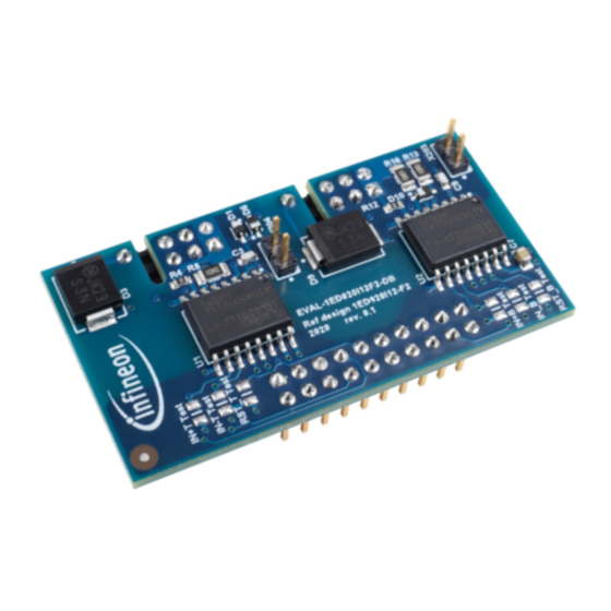
Page 5: The Board At A Glance
F2 with an integrated active Miller clamp preventing unintended turn-on and a DESAT pin to protect the application against damage through short circuit. Figure 1 and Figure 2 shows the daughterboard EVAL-1ED020I12F2-DB, Figure 3 shows the CoolSiC™ evaluation platform. Top view of evaluation daughterboard EVAL-1ED020I12F2-DB... - Page 6 Isolated driver daughter board to evaluate 1200 V CoolSiC™ MOSFET Fehler! Verwenden Sie die Registerkarte 'Start', um Heading 1;Heading1 dem Text zuzuweisen, der hier angezeigt werden soll. Bottom view of evaluation daughterboard EVAL-1ED020I12F2-DB Figure 2 A more detailed description please see in Chapter 1.2.
-
Page 7: Delivery Content
Figure 4 Delivery content Content of delivery is the EVAL-1ED020I12F2-DB board packed in a box. The evaluation platform EVAL-PS-DP- MAIN can be ordered seperatly. Since different daughterboards, such as EVAL-1ED020I12F2-DB, can be driven with one evaluation platform (motherboard), this arrangement allows a flexible choice of daughterboards with the motherboard. - Page 8 EVAL-1ED020I12F2-DB user guide Isolated driver daughter board to evaluate 1200 V CoolSiC™ MOSFET Fehler! Verwenden Sie die Registerkarte 'Start', um Heading 1;Heading1 dem Text zuzuweisen, der hier angezeigt werden soll. EVAL-1ED020I12F2-DB High-side X200 DESAT DESAT DESAT X202 DESAT VEE2_HS GND2_HS...
-
Page 9: Main Features
= 2 µs channel) Mechanical dimensions length width hight mm With connectors With respect to GND2 All this technical elctrical parameter shown in Table 2 are related to the Infineon gate driver IC 1ED020I12-F2. 9 of 28 v1.0 User Guide EVAL-1ED020I12F2-DB 2021-06-21... -
Page 10: System And Functional Desription
The connector X100 connect the primary side of the mainboard and the primary side of the EVAL-1ED020I12F2- DB which each other. All importand signals from EVAL-1ED020I12F2-DB like IN+, IN-, /Fault and /RDY of both drivers will be provided via X100 from the motherboard to the EVAL-1ED020I12F2-DB. At the motherboard side this signals are delivered from connector X101, which is the interface to the outside world, for example a µController. - Page 11 Isolated driver daughter board to evaluate 1200 V CoolSiC™ MOSFET Fehler! Verwenden Sie die Registerkarte 'Start', um Heading 1;Heading1 dem Text zuzuweisen, der hier angezeigt werden soll. Table 3 Jumper configurations for powersupply of EVAL-1ED020I12F2-DB +ADJ +20V -ADJ The settings for the adjustable driver voltages are made using the potentiometer R105 and R102 for the high-side driver and with potentiometer R108 and R107 for the low-side driver of the EVAL- 1ED020I12F2-DB.
-
Page 12: Description Of The Functional Blocks
Description of the functional blocks The description of the functional blocks of the daughterboard EVAL-1ED020I12F2-DB refer to Figure 5. All connections are shown only roughly, the detailed circuit is shown in Figure 8. In principle, the board can be separated into two parts, the primary and the secondary side. The primary side describes the low voltage area, the secondary the high-voltage area, which directly controls the power switch. - Page 13 EVAL-1ED020I12F2-DB user guide Isolated driver daughter board to evaluate 1200 V CoolSiC™ MOSFET Fehler! Verwenden Sie die Registerkarte 'Start', um Heading 1;Heading1 dem Text zuzuweisen, der hier angezeigt werden soll. 800 V Load X151 X152 X150 EVAL-1ED020I12F2-DB (daughter board) High-side...
-
Page 14: First Steps For Start Up
EVAL-1ED020I12F2-DB user guide Isolated driver daughter board to evaluate 1200 V CoolSiC™ MOSFET Fehler! Verwenden Sie die Registerkarte 'Start', um Heading 1;Heading1 dem Text zuzuweisen, der hier angezeigt werden soll. First steps for start up 2.2.2 Before the whole application can be put into operation, the following commissioning steps should be observed: 1.) Take empty motherboard out of the box... -
Page 15: System Design
Figure 8 Layout The following figures present the different layers of the layout from the daughterboard EVAL-1ED020I12F2-DB. Due to the small dimensions of the design, a 4-layer layout was provided. The order from the top view: Top layer, Layer 1, Layer 2, Bottom layer 15 of 28 v1.0... - Page 16 EVAL-1ED020I12F2-DB user guide Isolated driver daughter board to evaluate 1200 V CoolSiC™ MOSFET Fehler! Verwenden Sie die Registerkarte 'Start', um Heading 1;Heading1 dem Text zuzuweisen, der hier angezeigt werden soll. Top layer of EVAL-1ED020I12F2-DB Figure 9 Layer 1 of EVAL-1ED020I12F2-DB Figure 10 16 of 28 v1.0...
- Page 17 EVAL-1ED020I12F2-DB user guide Isolated driver daughter board to evaluate 1200 V CoolSiC™ MOSFET Fehler! Verwenden Sie die Registerkarte 'Start', um Heading 1;Heading1 dem Text zuzuweisen, der hier angezeigt werden soll. Layer 2 of EVAL-1ED020I12F2-DB Figure 11 Bottom layer of EVAL-1ED020I12F2-DB Figure 12 17 of 28 v1.0...
-
Page 18: Bill Of Material
Fehler! Verwenden Sie die Registerkarte 'Start', um Heading 1;Heading1 dem Text zuzuweisen, der hier angezeigt werden soll. Bill of material The complete bill of material is available on the download section of the Infineon homepage. A log-in is required to download this material. Table 4... -
Page 19: Connector Details
EVAL-1ED020I12F2-DB user guide Isolated driver daughter board to evaluate 1200 V CoolSiC™ MOSFET Fehler! Verwenden Sie die Registerkarte 'Start', um Heading 1;Heading1 dem Text zuzuweisen, der hier angezeigt werden soll. comment Ref Designator Description Manufacturer Manufacturer P/N Header, 2.54mm pitch,... - Page 20 EVAL-1ED020I12F2-DB user guide Isolated driver daughter board to evaluate 1200 V CoolSiC™ MOSFET Fehler! Verwenden Sie die Registerkarte 'Start', um Heading 1;Heading1 dem Text zuzuweisen, der hier angezeigt werden soll. Table 6 Connector X200 (High-side power switch – secondary side)
-
Page 21: System Performance
EVAL-1ED020I12F2-DB user guide Isolated driver daughter board to evaluate 1200 V CoolSiC™ MOSFET Fehler! Verwenden Sie die Registerkarte 'Start', um Heading 1;Heading1 dem Text zuzuweisen, der hier angezeigt werden soll. System performance In Chapter 4 some measurement results are introduced. These measurements are intended to demonstrate that the the system is fully operationa,l and that clear measurement data can be derived. -
Page 22: Example Measurement 1: Switching Resistive Load
EVAL-1ED020I12F2-DB user guide Isolated driver daughter board to evaluate 1200 V CoolSiC™ MOSFET Fehler! Verwenden Sie die Registerkarte 'Start', um Heading 1;Heading1 dem Text zuzuweisen, der hier angezeigt werden soll. output of the driver latching. This means the switch stays off, no matter what happens at switch off the the “IN”... -
Page 23: Example Measurement 2: Short Circuit At Low-Side
EVAL-1ED020I12F2-DB user guide Isolated driver daughter board to evaluate 1200 V CoolSiC™ MOSFET Fehler! Verwenden Sie die Registerkarte 'Start', um Heading 1;Heading1 dem Text zuzuweisen, der hier angezeigt werden soll. Figure 15 shows how the measurement works with an ohmic load resistor in a low-side configuration. As soon... -
Page 24: Example Measurement 3: Short Circuit At High-Side
EVAL-1ED020I12F2-DB user guide Isolated driver daughter board to evaluate 1200 V CoolSiC™ MOSFET Fehler! Verwenden Sie die Registerkarte 'Start', um Heading 1;Heading1 dem Text zuzuweisen, der hier angezeigt werden soll. Example measurement 3: short circuit at high-side 4.1.3 For a short-circuit measurement in the high-side configuration, the external circuitry of the system must be changed slightly, see Figure 17. - Page 25 EVAL-1ED020I12F2-DB user guide Isolated driver daughter board to evaluate 1200 V CoolSiC™ MOSFET Fehler! Verwenden Sie die Registerkarte 'Start', um Heading 1;Heading1 dem Text zuzuweisen, der hier angezeigt werden soll. Short ciruit measurement at high-side configuration Figure 18 The measurement results shown in Figure 18 are similar to result in Chapter 4.1.2, Figure 16. The difference is that the phase voltage V increases from zero up to approximat 620 V when Q1 is switched on.
-
Page 26: References And Appendices
EVAL-1ED020I12F2-DB user guide Isolated driver daughter board to evaluate 1200 V CoolSiC™ MOSFET Fehler! Verwenden Sie die Registerkarte 'Start', um Heading 1;Heading1 dem Text zuzuweisen, der hier angezeigt werden soll. References and appendices Abbreviations and definitions Table 8 Abbreviations Abbreviation Meaning Conformité... -
Page 27: Revision History
EVAL-1ED020I12F2-DB user guide Isolated driver daughter board to evaluate 1200 V CoolSiC™ MOSFET Revision history Revision history Document Date of release Description of changes version 27 of 28 v1.0 User Guide EVAL-1ED020I12F2-DB 2021-06-21... - Page 28 WARNINGS 81726 Munich, Germany Due to technical requirements products may contain dangerous substances. For information on the types in question please contact your nearest Infineon © 2021 Infineon Technologies AG. Technologies office. All Rights Reserved. Except as otherwise explicitly approved by Infineon...
- Page 29 Mouser Electronics Authorized Distributor Click to View Pricing, Inventory, Delivery & Lifecycle Information: Infineon EVAL1ED020I12F2DBTOBO1...
Need help?
Do you have a question about the EVAL-1ED020I12F2-DB and is the answer not in the manual?
Questions and answers