Table of Contents
Advertisement
Quick Links
STM32U575I-EV
User manual
Evaluation board with STM32U575AI MCU
Introduction
The
STM32U575I-EV
Evaluation board is designed as a complete demonstration and development platform for the
®
®
®
®
STMicroelectronics Arm
Cortex
-M33 core‑based microcontroller with Arm
TrustZone
and the Armv8-M mainline security
extension.
The STM32U575I-EV Evaluation board is based on an ultra-low-power
STM32U575AII6Q
microcontroller with 2 Mbytes of
Flash memory and 786 Kbytes of SRAM, one external memory interface supporting an LCD interface, two Octo‑SPI memory
®
interfaces, one USB Type-C
2.0 FS device and host with Power Delivery controller interface (UCPD) compliant with USB Type-
®
C
r1.2 and USB PD specification r3.0, one camera interface, one SDMMC interface, one 14-bit and one 12-bit ADCs, two
12-bit DACs, two operational amplifiers, two ultra‑low‑power comparators, four digital filters for sigma‑delta modulation, up to 16
timers, touchkey capability, and SWD, JTAG, and ETM interface debugging support.
The full range of hardware features on the STM32U575I-EV Evaluation board helps the user to develop applications and
®
evaluate all the peripherals, such as USB Type-C
connector with USB PD, motor control connector, CAN FD transceiver, USB
2.0 FS, RS-232, audio DAC, microphone ADC, dot-matrix TFT LCD, IrDA, IR LED, IR receiver, LDR, SRAM, camera interface,
™
2
Octo‑SPI Flash memory, microSD
card, sigma-delta modulators, smartcard slot, I
C, and EEPROM.
The daughterboard and extension connectors provide an easy way to connect a daughterboard or wrapping board for the user's
specific application.
Furthermore, the onboard STLINK-V3E debugger provides out‑of‑the‑box loading and debugging capabilities, as well as a USB
Virtual COM port bridge.
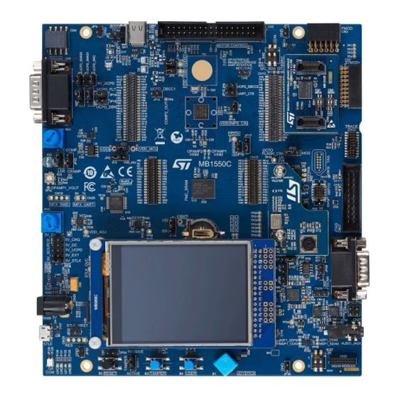
Figure 1.
STM32U575I-EV Evaluation board (top view)
Figure 2.
STM32U575I-EV Evaluation board (bottom view)
Pictures are not contractual.
UM2854 - Rev 1 - September 2021
www.st.com
For further information contact your local STMicroelectronics sales office.
Advertisement
Table of Contents

Related Manuals for ST STM32U575I-EV


Summary of Contents for ST STM32U575I-EV
-
Page 1: Figure 1. Stm32U575I-Ev Evaluation Board (Top View)
12-bit DACs, two operational amplifiers, two ultra‑low‑power comparators, four digital filters for sigma‑delta modulation, up to 16 timers, touchkey capability, and SWD, JTAG, and ETM interface debugging support. The full range of hardware features on the STM32U575I-EV Evaluation board helps the user to develop applications and ®... -
Page 2: Features
FS, Sink and Source power capability 5 V / 500 mA • SAI audio codec • ST-MEMS digital microphone • ST-MEMS 3D accelerometer and 3D gyroscope sensor • Light-dependent resistor (LDR) and potentiometer for ADC • 512-Mbit Octo‑SPI Flash, 16-Mbit SRAM, 128-Kbit I C EEPROM •... -
Page 3: Ordering Information
STM32U575I-EV Ordering information Ordering information To order the STM32U575I-EV Evaluation board, refer to Table 1. Additional information is available from the datasheet and reference manual of the target STM32. Table 1. List of available products Order code Board reference Target STM32 •... -
Page 4: Development Environment
STM32 Flash memory for easy demonstration of the device peripherals in standalone mode. The latest versions of the demonstration source code and associated documentation can be downloaded from www.st.com. UM2854 - Rev 1 page 4/105... -
Page 5: Conventions
STM32U575I-EV Conventions Conventions Table 3 provides the conventions used for the ON and OFF settings in the present document. Table 3. ON/OFF convention Convention Definition Jumper JPx ON Jumper fitted Jumper JPx OFF Jumper not fitted Jumper JPx [1-2] Jumper fitted between Pin 1 and Pin 2 Solder bridge SBx ON SBx connections closed by 0 Ω... -
Page 6: Delivery Recommendations
STM32U575I-EV Delivery recommendations Delivery recommendations Before the first use, make sure that no damage occurred to the board during shipment and no socketed components are loosened in their sockets or fallen into the plastic bag. In particular, pay attention to the following components: The MB989 LCD daughterboard is in its CN23 connector, and the LCD screw, spacer, and nut are in place. -
Page 7: Getting Started
® Connect the STM32U575I-EV Evaluation board to a PC with a USB Type-A or USB Type-C to Micro-B cable through the CN26 STLINK-V3E USB connector to power the board. The LD2 green LED (5V_PWR) lights up and the LD4 (COM) blinks. -
Page 8: Hardware Layout And Configuration
STM32U575I-EV Hardware layout and configuration Hardware layout and configuration Hardware block diagram and board layout The STM32U575I-EV Evaluation board is designed around the STM32U575AII6Q target microcontroller. Figure 3 illustrates STM32U575AII6Q connections with peripheral components. Figure 4 shows the location of the main... -
Page 9: Figure 4. Stm32U575I-Ev Pcb Layout (Top View)
STM32U575I-EV Hardware block diagram and board layout Figure 4. STM32U575I-EV PCB layout (top view) Figure 5. STM32U575I-EV PCB layout (bottom view) UM2854 - Rev 1 page 9/105... -
Page 10: Default Board Configuration
Default board configuration By default, the STM32U575I-EV Evaluation board is configured with VDD_MCU at 3.3 V. It is possible to set the board with VDD_MCU at 1.8 V. Before switching to 1.8 V, check that the extension module and external shield connected to the STM32U575I-EV Evaluation board are 1.8 V compatible. -
Page 11: Figure 7. Switch Default Board Configuration
STM32U575I-EV Default board configuration Figure 7 summarizes the switch default settings of the STM32U575I-EV Evaluation board. Figure 7. Switch default board configuration UM2854 - Rev 1 page 11/105... -
Page 12: Table 4. Jumper Default Settings
STM32U575I-EV Default board configuration Table 4 describes the default jumper setting. Table 4. Jumper default settings Jumper Function Setting Comment GND probe GND probe GND probe GND probe BOOTLOADER_BOOT0 from USART Boot 0 from USART not connected VDDIO power source selection... -
Page 13: Embedded Stlink-V3E
PB15 Not used 7.3.2 Drivers Before connecting the STM32U575I-EV Evaluation board to a Windows PC via USB, the user must install a driver for the STLINK-V3E (not required for Windows 10). It is available on the www.st.com website. In case the STM32U575I-EV Evaluation board is connected to the PC before the driver is installed, some STM32U575I-EV Evaluation board interfaces may be declared as Unknown in the PC device manager. -
Page 14: Stlink-V3E Firmware Upgrade
STM32U575I-EV Evaluation board and periodically, to stay up-to-date with the latest firmware version. 7.3.4 Using an external debugging tool to program and debug the on-board STM32 There are 2 basics ways to support an external Debug tool: Keep the embedded STLINK-V3E running. -
Page 15: Stdc14/Mipi-10 Connector
STM32U575I-EV STDC14/MIPI‑10 connector STDC14/MIPI‑10 connector 7.4.1 Description CN18 5x2-pin 1.27 mm pitch header connector compatible with STDC14 can output JTAG signals used for debugging. The CN18 footprint supports the STDC14 interface and also the MIPI‑10 interface. By default, only a MIPI‑10 connector is present. -
Page 16: Figure 10. Cn18 Stdc14 Connector Pinout
STM32U575I-EV STDC14/MIPI‑10 connector Figure 10 shows the CN18 STDC14 connector pinout. Figure 10. CN18 STDC14 connector pinout UM2854 - Rev 1 page 16/105... -
Page 17: I/O Restriction To Other Features
STM32U575I-EV STDC14/MIPI‑10 connector Table 7 describes the STDC14/MIPI‑10 connector pinout compatible with both STDC14 and MIPI-10 interfaces. Table 7. CN18 STDC14/MIPI‑10 debug connector pinout STDC14 MIPI‑10 pin STM32 pin Board function Reserved Reserved Target VDD JTMS_SWDIO: Target SWDIO using SWD protocol or Target JTMS using JTAG... -
Page 18: Tag Footprint
STM32U575I-EV TAG footprint TAG footprint 7.5.1 Description The CN13 footprint can also output a debug interface compatible with the TAG probe TC2050-IDC-NL. Table 8 describes the hardware configuration for the TAG function. Table 8. Hardware I/O configuration for the CN13 TAG connector... -
Page 19: I/O Restriction To Other Features
STM32U575I-EV TAG footprint Table 9 describes the CN13 TAG connector pinout. Table 9. CN13 TAG connector pinout Connector STM32 pin Board function pin number Power PA13 JTMS_SWDIO: Target SWDIO using SWD protocol or Target JTMS using JTAG protocol Power PA14... -
Page 20: Etm Trace
STM32U575I-EV ETM trace ETM trace 7.6.1 Description CN12 header 10x2-pin 1.27 mm pitch connector can output trace signals used to debug. Table 10 describes the hardware configuration for the TRACE function. Table 10. Hardware I/O configuration for the CN12 TRACE connector... -
Page 21: Figure 12. Cn12 Trace Connector Pinout
STM32U575I-EV ETM trace Figure 12 shows the TRACE connector pinout. Figure 12. CN12 TRACE connector pinout UM2854 - Rev 1 page 21/105... -
Page 22: I/O Restriction To Other Features
STM32U575I-EV ETM trace Table 11 describes the TRACE connector pinout. Table 11. CN12 TRACE connector pinout Connector STM32 pin Board function pin number Power PA13 JTMS_SWDIO: Target SWDIO using SWD protocol or Target JTMS using JTAG protocol Power PA14 JTCK_SWCLK: Target SWCLK using SWD protocol or Target JTCK using JTAG protocol... -
Page 23: Jtag Connector
STM32U575I-EV JTAG connector JTAG connector 7.7.1 JTAG connector The CN17 header 10x2-pin 2.54 mm pitch connector can output JTAG signals used to debug. Table 12 describes the hardware configuration for the JTAG function. Table 12. Hardware I/O configuration for the JTAG function on CN17 connector... -
Page 24: I/O Restriction To Other Features
STM32U575I-EV JTAG connector Table 13. CN17 JTAG connector pinout describes the JTAG connector pinout. Table 13. CN17 JTAG connector pinout Connector STM32 pin Board function pin number Power Power JTRSTN: JTAG RESET protocol Power PA15 JTDI: Not used by SWD protocol, Target JTDI using JTAG protocol, only for external tools... -
Page 25: Power Supply
5 V power supply general view The STM32U575I-EV Evaluation board is designed to be powered from a 5 V DC power source. One of the following five 5 V DC power inputs can be used, upon an appropriate board configuration: •... -
Page 26: 5V_Stlk Power Source
STLINK-V3E circuit has the power before USB enumeration, as the host PC only provides 100 mA to the board at that time. During the USB enumeration, the STM32U575I-EV board asks for the 500 mA power to the host PC. -
Page 27: 5V_Ext Power Source
STM32U575I-EV Power supply 7.8.3 5V_EXT power source 5V_EXT is the DC power coming from the CN25 power jack. In this case, the JP25 jumper must be on pin [3-4] to select the 5V_EXT power source. The positive pole is on the center pin as illustrated in... -
Page 28: 5V_Ucpd Power Source
STM32U575I-EV Power supply 7.8.4 5V_UCPD power source ® 5V_UCPD is the DC power supply connected to the CN1 user USB Type-C . In this case, the JP25 jumper must be set on [5-6] to select the 5V_UCPD power source. 5V_UCPD power source configuration for the JP25 jumper is described in Figure Figure 17. -
Page 29: 5V_Dc Power Source
STM32U575I-EV Power supply 7.8.5 5V_DC power source 5V_DC is the DC power coming from external (5V DC power from CN9 extension connector pin 49. In this case, the JP25 jumper must be on pin [7-8] to select the 5V_DC power source. -
Page 30: 5V_Chg Power Source
5V_CHG is the DC power charger connected to CN26 USB STLINK-V3E. In this case, the JP25 jumper must be set on [9-10] to select the 5V_CHG power source. If the STM32U575I-EV board is powered by an external USB charger, then the debug is not available. If a computer is connected instead of the charger, the current limitation is no more effective. -
Page 31: Programing/Debugging When The Power Supply Is Not From Stlink-V3E (5V_Stlk)
Regardless of the 5V power source, the U19 LDO is used to deliver a fixed 3.3 V power supply, with a current capability of 1.3 A. This power source of 3.3 V is shared between the STM32U575I-EV and its expansion boards. -
Page 32: Vdd_Mcu Idd Measurement
ULPBench probe, where only VDD_MCU is externally powered, (meaning No STLINK, no 5V, no VDD, only JP19 pin 2 powered by 3V3 or 1V8), it is recommended to configure the STM32U575I-EV Evaluation board to avoid leakage currents from I/Os connected to unpowered components. This configuration can be used to assure there is no return consumption from other power sources such as VDD_MCU. -
Page 33: Table 16. Hardware Configuration For The Mcu Power Supply Voltage
STM32U575I-EV Power supply Table 16 details the MCU power supply configuration and the associated hardware configuration. Table 16. Hardware configuration for the MCU power supply voltage Jumper Definition Setting Comment JP23[1-2] VDD source is fixed at 3.3V. VDD source selection JP23 Range 1.7 V <... -
Page 34: Figure 20. Jumpers And Solder Bridges For Power Sources
STM32U575I-EV Power supply Figure 20 describes the MCU power supplied position on the STM32U575I-EV board. Figure 20. Jumpers and solder bridges for power sources UM2854 - Rev 1 page 34/105... -
Page 35: Clock References
STM32U575I-EV Clock references Clock references Two clock references are available on STM32U575I-EV for the STM32U575AII6Q target microcontroller. • 32.768 kHz crystal X2, for LSE embedded RTC • 16 MHz crystal X1, for HSE clock generator. The main clock can also be generated using an internal RC oscillator. -
Page 36: Reset Sources
7.11.1 Description The bootloader is located in the system memory, programmed by ST during production. It is used to reprogram the Flash memory by using USART, I C, SPI, CAN FD, or USB FS in device mode through the DFU (device firmware upgrade). -
Page 37: Audio
A codec CS42L51-CNZ is connected to the SAI interface of STM32U575AII6Q which supports the TDM feature of the SAI port. The TDM feature offers STM32U575AII6Q the capability to stream stereo audio channels. There is also one digital microphone on the STM32U575I-EV Evaluation board, which offers the possibility to connect a MEMS extension daughterboard. -
Page 38: Headphones Outputs
7.12.5 Headphones outputs The STM32U575I-EV Evaluation board can drive stereo headphones. The STM32U575AII6Q sends up the stereo audio channels, via its SAI1 TDM port, to the codec device. The codec device converts the digital audio stream to stereo analog signals. It then boosts them for direct drive of headphones connecting to CN27 3.5 mm stereo jack receptacles on the board. -
Page 39: I/O Restriction To Other Features
When a USB host connection to the CN1 USB Type-C connector of STM32U575I-EV Evaluation board is detected, the STM32U575I-EV Evaluation board starts behaving as a USB device. Depending on the powering capability of the USB host, the board can take power from the V terminal of CN1. -
Page 40: Ucpd
UCPD ® USB Type-C introduces the USB Power Delivery feature. STM32U575I-EV Evaluation board supports the dead battery, the SINK mode, and the SOURCE mode. The fast role swap (FRS) is optional. ® In addition to the DP/DM I/Os directly connected to the USB Type-C... -
Page 41: Usb Type-C Connector
STM32U575I-EV USB Type-C® FS port Hardware Setting Configuration PB11 is used as I2C_SDA to interface the port protection and is PB11 SB49 shared with MFX, touch panel, Ext_I2C, EEPROM, 3D accelerometer, 3D gyroscope, camera, and STMod+. UCPD_DBCC1 is connected to GND for UCPD DB function through the... -
Page 42: I/O Restriction To Other Features
7.14 RS-232 port 7.14.1 RS-232 port The STM32U575I-EV Evaluation board offers one RS-232 communication port. The RS-232 communication port uses the CN6 DB9 male connector. 7.14.2 Operating voltage The U43 RS-232 transceiver is supplied by the fixed 3V3 power voltage. To support the MCU 1V8 I/O configuration, the U45 level shifter is used for the MCU output I/O to reach the transceiver voltage input high level (VIH). -
Page 43: Table 27. Hardware I/O Configuration For The Rs-232 Interface
STM32U575I-EV RS-232 port Table 27 describes the hardware configuration for the RS-232 interface. Table 27. Hardware I/O configuration for the RS-232 interface Hardware Setting Configuration PG7 LPUART1_TX is NOT connected to the RS-232 transceiver [1-2] PG7 is used as LPBAM I2C or UCPD_FRSCC2... -
Page 44: I/O Restriction To Other Features
STM32U575I-EV RS-232 port Table 28 describes the CN6 RS-232 connector pinout. Table 28. CN6 RS-232 connector pinout Connector pin STM32 pin Board function number RXD / UART_RX from MCU TXD / UART_TX from MCU PH3_BOOT0 DSR / used as external input for BOOT0 pin driving... -
Page 45: Microsd™ Card
STM32U575I-EV microSD™ card 7.15 ™ microSD card 7.15.1 Description ™ The CN30 slot for the microSD card is routed to the STM32U575AII6Q SDIO port. This interface is compliant with SD Memory Card Specification Version 6.0: SDR104 SDMMC_CK speed limited to the maximum allowed I/O ™... -
Page 46: I/O Restriction To Other Features
STM32U575I-EV microSD™ card Figure 24 shows the CN30 SD card connector pinout. Figure 24. CN30 SD card connector pinout Table 30 describes the CN30 SD card connector pinout. Table 30. CN30 SD card connector pinout Connector pin STM32 pin Board function... -
Page 47: Can Fd
7.16 CAN FD 7.16.1 Description The STM32U575I-EV Evaluation board supports one CAN FD compliant with ISO-11898-1 version 2.0 parts A and B. The CN22 DB9 male connector is available as a CAN‑FD interface. 7.16.2 Operating voltage A 3.3 V CAN transceiver is fitted between the CN22 connector and the CAN‑FD controller port of STM32U575AII6Q. -
Page 48: I/O Restriction To Other Features
7.17 Smartcard 7.17.1 Description The STM32U575I-EV Evaluation board supports one smartcard interface. The CN31 smartcard connector is used as a card reader. The smartcard interface is on the bottom side of the board. 7.17.2 Operating voltage The smartcard interface is only compatible with the 2.7 to 3.6 V MCU voltage range. Low power MCU 1.8 V is not supported by the smartcard interface. -
Page 49: Smartcard Interface
STM32U575I-EV Smartcard 7.17.3 Smartcard interface A smartcard interface is used between the CN31 card reader connector and the smartcard controller port of STM32U575AII6Q. Table 33 describes the hardware configuration for the smartcard interface. Table 33. Hardware I/O configuration for the smartcard interface... -
Page 50: I/O Restriction To Other Features
STM32U575I-EV User LEDs Table 34 describes the U31 smartcard interface and CN31 connector pinout. Table 34. U31 smartcard interface and CN31 connector pinout Board function transceiver 17 VCC Smartcard power supply 16 RST Smartcard reset 15 CLK Smartcard clock 13 AUX1... -
Page 51: Led Interface
1. The default configuration is shown in bold. 7.19 Physical input devices: buttons 7.19.1 Description The STM32U575I-EV Evaluation board provides several input devices for physical human control. These are: • B1 four‑way joystick controller with a selection key • B2 reset button •... -
Page 52: Physical Input I/O Interface
STMOD+_INT or the motor‑control functions. The user button function cannot be operated simultaneously with the active tamper function. 7.20 Operational amplifiers and comparator 7.20.1 Description The STM32U575I-EV Evaluation board offers the possibility to test the internal operational amplifiers and comparators according to: • RV1 10 kΩ potentiometer • R33 LDR light‑dependent resistor The potentiometer and light-dependent resistor can be mutually exclusively routed to either PB4 (Comp) or PA0 (OpAmp) port of STM32U575AII6Q. -
Page 53: Comparator
7.20.4 Comparator STM32U575AII6Q provides two onboard comparators. One of which, Comp2, is made accessible on the STM32U575I-EV Evaluation board. Comp2 has its non-inverting input and its output. Table 39 describes the hardware configuration for the comparator interface. UM2854 - Rev 1... -
Page 54: I/O Restriction To Other Features
The input is accessible on pin 1 of the JP22 jumper header. On top of the possibility of routing either the potentiometer or LDR to PB4, an external source can also be connected to it, using JP22 terminal 1. The PB5 output of the comparator can be accessed on test point TP9. Refer to the schematic of STM32U575I-EV Evaluation board. -
Page 55: I/O Restriction To Other Features
SRAM device 7.22.1 Description A 16-Mbit static RAM (SRAM), 1 M x16 bit, is fitted on the STM32U575I-EV Evaluation board in the U12 position. 7.22.2 Operating voltage The SRAM is only functional in the voltage range from 2.4 to 3.6 V, according to the SRAM datasheet. This SRAM does not support the 1.8 V MCU low voltage. -
Page 56: Table 43. Hardware I/O Configuration For The Sram Interface
STM32U575I-EV SRAM device Table 43. Hardware I/O configuration for the SRAM interface Hardware Setting Configuration R202 PD7 is used as FMC_NE1 and connected to SRAM R210 PD5 is used as FMC_NWE and connected to SRAM and LCD R216 PD4 is used as FMC_NOE and connected to SRAM and LCD... -
Page 57: I/O Restriction To Other Features
I/O restriction to other features By default, only an SRAM of 16 Mbits is present on the STM32U575I-EV Evaluation board. An update of the SRAM (footprint compatible) is possible to increase the memory up to 32 MBits A[0-20]. The FMC interface is shared with LCD. -
Page 58: Octo-Spi2 Flash I/O Interface
STM32U575I-EV Octo‑SPI2 Flash memory device 7.23.3 Octo‑SPI2 Flash I/O interface Table 44 describes the hardware configuration for the Octo‑SPI2 interface. Table 44. Hardware I/O configuration for the Octo‑SPI2 Flash interface Hardware Setting Configuration PI5 is connected to Octo-SPI2 FLASH as NCS... -
Page 59: Octo-Spi1
7.24.1 Description The STM32U575I-EV Evaluation board embeds the possibility to evaluate more Octo‑SPI memory devices. Two 2x10‑pin high‑speed socket connectors are available to support the MB1242 ST memory daughterboard. One MB1242 with Octo‑SPI PSRAM memory is included on the STM32U575I-EV Evaluation board. -
Page 60: Figure 27. Cn5/Cn11 Octo-Spi Connector Pinout
STM32U575I-EV Octo‑SPI1 Hardware Setting Configuration PC1 is NOT connected to Octo‑SPI1. R163 PC1 can be used for motor control. PC2 is connected to Octo‑SPI1 as IO5. R162 PC2 is NOT connected to Octo‑SPI1. PC2 can be used for motor control. -
Page 61: Table 46. Cn11 Octo-Spi Connector Pinout
STM32U575I-EV Octo‑SPI1 Table 46 describes the CN11 Octo‑SPI connector pinout Table 46. CN11 Octo‑SPI connector pinout Connector pin STM32 pin Board function number Octo‑SPI chip select interface low level. mainly for Octo‑SPI Flash memory configuration. This signal is connected to a 10K pull-up on board (R23). -
Page 62: I/O Restriction To Other Features
7.25.1 Description The 128-Kbit I C‑bus EEPROM device is fitted on the STM32U575I-EV Evaluation board in the U8 position. It is accessed with STM32U575AII6Q I C‑bus lines I2C_SCL and I2C_SDA. EEPROM write‑protection is possible when the SB2 solder bridge is OFF. SB2 is ON by default and writing into the EEPROM is enabled. -
Page 63: Eeprom I/O Interface
The EXT_I2C connector can accept a daughterboard that can have a different I C base address. Be careful not to use a daughterboard with an I C base address already used in the STM32U575I-EV Evaluation board to avoid C conflict. UM2854 - Rev 1... -
Page 64: Table 49. Hardware I/O Configuration For The Ext_I2C Connector
STM32U575I-EV EXT_I2C connector Table 49 describes the hardware configuration for the EXT_I2C connector. Table 49. Hardware I/O configuration for the EXT_I2C connector Hardware Setting Configuration PG8 is used as I2C3_SDA to interface the sensor like the 3D [1-2] accelerometer and the 3G gyroscope, but also the I... -
Page 65: Touchkey Button
7.27 Touchkey button 7.27.1 Description The STM32U575I-EV Evaluation board supports a touchkey button based on either RC charging or charge- transfer technique. This one is enabled by default. 7.27.2 Touchkey button I/O interface The touchkey button is connected to one of the TSC ports of STM32U575AII6Q with the related charge capacitor. -
Page 66: I/O Restriction To Other Features
7.28 MFX MCU 7.28.1 Description The multi-function expander MFX MCU is used as a GPIO-expander and is fitted on the STM32U575I-EV Evaluation board in U15 position. 7.28.2 Operating voltage The MFX MCU is connected to VDD and is fully compatible with the 1.71 to 3.6 V MCU voltage range. -
Page 67: Table 52. Hardware I/O Configuration For The Mfx Interface
STM32U575I-EV MFX MCU Table 52 describes the hardware configuration for the MFX interface. Table 52. Hardware I/O configuration for the MFX interface Hardware Setting Configuration PC5 is connected to MFX as MFX_IRQ_OUT. SB70 No other muxing PF11 is connected to MFX as MFX_WAKEUP. -
Page 68: Tft Lcd
STM32U575I-EV TFT LCD 7.29 TFT LCD 7.29.1 Description The CN23 34‑pin 2.54 mm pitch female connector is designed to connect the MB989 TFT LCD daughterboard supporting the FMC interface to the MB1550 mother board. The LCD daughterboard is composed of the TFT LCD daughterboard supporting a resolution of 240 x 320 dots 262K colors and a touch-panel feature driven by MFX in U15 position. - Page 69 STM32U575I-EV TFT LCD Hardware Setting Configuration PB10 is used as I2C2_SCL to interface the audio codec, MFX, UCPD, CTP, camera, STMod+, and optionally sensors like the 3D accelerometer PB10 SB46 and the 3G gyroscope but also the I C EEPROM and the external I...
-
Page 70: Figure 29. Cn23 Lcd Connector Pinout
STM32U575I-EV TFT LCD Figure 29 shows the CN23 LCD connector pinout. Figure 29. CN23 LCD connector pinout UM2854 - Rev 1 page 70/105... -
Page 71: Table 55. Lcd Connector Pinout
STM32U575I-EV TFT LCD Table 55 describes the CN23 LCD connector pinout Table 55. LCD connector pinout Connector pin STM32 pin Board function number PG12 FMC_NE4_LCD_CSn: Chip Select function (active low) FMC_A22_LCD_RS: Register Select signal FMC_NWE: Write enable signal active high... -
Page 72: I/O Restriction To Other Features
STM32U575I-EV Camera 7.29.4 I/O restriction to other features Caution: Due to the sharing of some I/Os of STM32U575AII6Q by multiple peripherals, the following limitations apply in using the LCD feature: • FMC interface is shared with SRAM. 7.30 Camera 7.30.1 Description The CN16 40‑pin 1.00 mm pitch female connector is designed to connect the MB1379 CMOS camera... -
Page 73: Table 56. Hardware I/O Configuration For The Camera Interface
STM32U575I-EV Camera Table 56 describes the hardware configuration for the camera interface. Table 56. Hardware I/O configuration for the camera interface Hardware Setting Configuration PG10 is used as CAMERA PLUG. Detection of the camera daughterboard presence. PG10 SB103 PG10 can be used for STMod+. -
Page 74: Figure 30. Cn16 Camera Connector Pinout
STM32U575I-EV Camera Figure 30 shows the CN16 camera connector pinout. Figure 30. CN16 camera connector pinout Table 57 describes the CN16 camera daughterboard connector pinout UM2854 - Rev 1 page 74/105... -
Page 75: Table 57. Camera Connector Pinout
STM32U575I-EV Camera Table 57. Camera connector pinout Connector pin STM32 pin Board function number Not used Not used Power GND Power GND Not used Not used Power GND Power GND Not used Not used Power GND Power GND PB10 I2C_SCL_CAMERA... -
Page 76: I/O Restriction To Other Features
7.31.1 Description ™ The CN3 standard 12-pin Pmod connector is available on the STM32U575I-EV Evaluation board to support ™ low frequency, low I/O pin count peripheral daughterboards. The Pmod interface which is implemented on ™ the STM32U575I-EV Evaluation board is compatible with the Pmod type 2A and 4A I/O signal assignment convention. -
Page 77: Table 59. Hardware I/O Configuration For The Pmod ™ Interface
STM32U575I-EV Pmod™ connector ™ Table 59 describes the hardware configuration for the Pmod interface. ™ Table 59. Hardware I/O configuration for the Pmod interface Hardware Configuration Setting ™ PA4 is used as SPI_NSS on Pmod and shared with STMod+ and ADC/ DAC. -
Page 78: I/O Restriction To Other Features
STM32U575I-EV Pmod™ connector ™ Figure 31 shows the CN3 Pmod connector pinout. ™ Figure 31. CN3 Pmod connector pinout ™ Table 60 describes the CN3 Pmod connector pinout ™ Table 60. Pmod connector pinout Connector pin STM32 pin Board function... -
Page 79: Stmod+ Connector
7.32.2 Operating voltage The STMod+ connector is directly supplied by 5 V. The STM32U575I-EV Evaluation board I/O level can be set according to the 3.3 V STMod+ connector. The fan-out board also embeds a 3.3 V regulator and I C level shifters. -
Page 80: Table 62. Hardware I/O Configuration For The Stmod+ Interface
STM32U575I-EV STMod+ connector Table 62. Hardware I/O configuration for the STMod+ interface Hardware Setting Configuration ™ PA4 is used as SPI_NSS on STMod+ and shared with Pmod and ADC/ DAC. SB18 PA4 is not used as SPI_NSS on STMod+. PA4 can be used for Motor control or to ADC/DAC ™... -
Page 81: Figure 32. Cn7 Stmod+ Connector Pinout
STM32U575I-EV STMod+ connector Hardware Setting Configuration ™ PA1 is used as PMOD_INT on STMod+ and shared with Pmod ON/ON TAMPER_KEY SB71/R135 PA1 is not used as STMOD+_INT on STMod+. OFF/OFF PA1 can be used for Tamper_Key or motor control. ™... -
Page 82: I/O Restriction To Other Features
STM32U575I-EV Motor control Table 63 describes the CN7 STMod+ connector pinout. Table 63. CN7 STMod+ connector pinout Connector pin STM32 pin Board function number PA4 / PB13 SPI_NSS / LPUART1_CTS PC12 / PG7 SPI3_MOSI / UART_TX PG10 / PG8 SPI3_MISO / UART_RX... -
Page 83: Motor-Control I/O Interface
STM32U575I-EV Motor control 7.33.2 Motor‑control I/O interface The motor‑control I/O interface is not connected by default, because it is too high I/O consuming. Table 64 describes the assignment of the motor‑control interface and the I/O function associated with STM32U575AII6Q. Table 64. - Page 84 STM32U575I-EV Motor control CN2 motor‑control connector STM32U575AII6Q microcontroller Alternate Board modification for Terminal Terminal name Port name Function function enabling motor control PhaseC current- Close SB107 ICL Shutout GPIO Open SB108 STMod+ or no daughterboard Close SB45 Dissipative Brake GPIO Remove R148 (Octo‑SPI)
-
Page 85: I/O Restriction To Other Features
STM32U575I-EV CN9, CN10, CN14, and CN15 extension connectors Figure 33 shows the CN2 motor‑control connector pinout. Figure 33. CN2 motor‑control connector pinout 7.33.3 I/O restriction to other features Caution: Due to the sharing of some I/Os of STM32U575AII6Q by multiple peripherals, the following limitations apply in using the motor‑control feature:... -
Page 86: Table 65. Cn9 Connector Pinout
STM32U575I-EV CN9, CN10, CN14, and CN15 extension connectors Figure 34 shows the CN9 and CN10 connector pinout. Figure 34. CN9 and CN10 connector pinout Table 65 describes the CN9 connector pinout. Table 65. CN9 connector pinout Connector STM32 pin Default board function... -
Page 87: Table 66. Cn10 Connector Pinout
STM32U575I-EV CN9, CN10, CN14, and CN15 extension connectors Connector STM32 pin Default board function Optional board function pin number UCPD_FLT, MDF1_CCK0 FDCAN_RX UCPD_DBn FDCAN_TX PB10 I2C2_SCL PB11 I2C2_SDA PB13 SHIELD UART_CTS PB14 SHIELD_CS USB_DBCC2 PC13 USER BUTTON ACTIVE TAMPER PB15... - Page 88 STM32U575I-EV CN9, CN10, CN14, and CN15 extension connectors Connector STM32 pin Default board function Optional board function pin number PA14 SWCLK, JTCK OCTOSPI2_IO2 OCTOSPI2_IO1, CAMERA_RSTI OCTOSPI2_IO0, CAMERA_XSDN DCMI_D5 OCTOSPI2_NCS, DCMI_VSYNC POWER GND DCMI_D7 DCMI_D6 OCTOSPI2_DQS DCMI_PIXCLK OCTOSPI2_CLK OCTOSPI2_IO3, DCMI_HSYNC OCTOSPI2_IO4, DCMI_D0...
-
Page 89: Table 67. Cn14 Connector Pinout
STM32U575I-EV CN9, CN10, CN14, and CN15 extension connectors Connector STM32 pin Default board function Optional board function pin number PC10 SDIO_D2, TRACE_D1 PC11 SDIO1_D3 PC12 SDIO1_CLK, SPI3_MOSI, TRACE_D3 SDIO1_CMD POWER GND POWER 5 V 1. Exclusive when several are connected by default. -
Page 90: Table 68. Cn15 Connector Pinout
STM32U575I-EV CN9, CN10, CN14, and CN15 extension connectors Connector STM32 pin Default board function Optional board function pin number MDF1_SDIN3 FMC_A20 SPI3_SCK TRACE_D2 FMC_NE1 FMC_A22_LCD_RS SAI1_SD_A FMC_A0 FMC_NWE FMC_A1 FMC_NOE FMC_A2 MDF1_SDIN0 FMC_A3 FMC_D3 FMC_A4 FMC_D2 FMC_A5 POWER GND POWER GND POWER VDD POWER 3.3 V... - Page 91 STM32U575I-EV CN9, CN10, CN14, and CN15 extension connectors Connector pin STM32 pin Board function number PD10 FMC_D15 FMC_D5 PD11 FMC_A16 FMC_D4 PD12 FMC_A17 FMC_A11 PD13 FMC_A18 FMC_A10 PD14 FMC_D0 PF15 FMC_A9 PD15 FMC_D1 PF14 FMC_A8 FMC_A12 PF13 FMC_A7 FMC_A13 PF12...
-
Page 92: Stm32U575I-Ev Evaluation Board Information
Evaluation tools marked as “ES” or “E” are not yet qualified and therefore not ready to be used as reference design or in production. Any consequences deriving from such usage will not be at ST charge. In no event, ST will be liable for any customer usage of these engineering sample tools as reference designs or in production. -
Page 93: Board Mb1242 Revision B01
STM32U575I-EV Board revision history 8.3.3 Board MB1242 revision B01 Board limitations No limitation identified for this board revision. 8.3.4 Board MB1379 revision A05 Board limitations No limitation identified for this board revision. UM2854 - Rev 1 page 93/105... -
Page 94: Federal Communications Commission (Fcc) And Innovation, Science And Economic
STM32U575I-EV Federal Communications Commission (FCC) and Innovation, Science and Economic Development Canada (ISED) Compliance Statements Federal Communications Commission (FCC) and Innovation, Science and Economic Development Canada (ISED) Compliance Statements FCC Compliance Statement Part 15.19 This device complies with Part 15 of the FCC Rules. Operation is subject to the following two conditions: (1) this device may not cause harmful interference, and (2) this device must accept any interference received, including interference that may cause undesired operation. -
Page 95: Ce Conformity
STM32U575I-EV CE conformity CE conformity 10.1 Warning EN 55032 / CISPR32 (2012) Class A product Warning: this device is compliant with Class A of EN55032 / CISPR32. In a residential environment, this equipment may cause radio interference. Avertissement : cet équipement est conforme à la Classe A de la EN55032 / CISPR 32. Dans un environnement résidentiel, cet équipement peut créer des interférences radio. -
Page 96: Revision History
STM32U575I-EV Revision history Table 69. Document revision history Date Revision Changes 22-Sep-2021 Initial release. UM2854 - Rev 1 page 96/105... -
Page 97: Table Of Contents
STM32U575I-EV Contents Contents Features................2 Ordering information . - Page 98 STM32U575I-EV Contents 7.8.5 5V_DC power source ........... . 29 7.8.6...
- Page 99 STM32U575I-EV Contents 7.16.1 Description ............47 7.16.2...
- Page 100 STM32U575I-EV Contents 7.24 Octo‑SPI1..............59 7.24.1...
- Page 101 STM32U575I-EV Evaluation board information........92...
-
Page 102: List Of Tables
STM32U575I-EV List of tables List of tables Table 1. List of available products............. . . 3 Table 2. - Page 103 STM32U575I-EV List of tables Table 54. Hardware I/O configuration for the LCD and CTP interface ........68 Table 55.
-
Page 104: List Of Figures
STM32U575I-EV Evaluation board (bottom view) ........ - Page 105 ST’s terms and conditions of sale in place at the time of order acknowledgement. Purchasers are solely responsible for the choice, selection, and use of ST products and ST assumes no liability for application assistance or the design of Purchasers’...
Need help?
Do you have a question about the STM32U575I-EV and is the answer not in the manual?
Questions and answers