Table of Contents
Advertisement
Quick Links
One Technology Way • P.O. Box 9106 • Norwood, MA 02062-9106, U.S.A. • Tel: 781.329.4700 • Fax: 781.461.3113 • www.analog.com
FEATURES
Full featured evaluation system for the
2-layer PCB (4" × 5" form factor)
9 V power supply regulated to 3.3 V on board
4-pin UART header to connect to RS-232 interface cable
20-pin standard JTAG connector
Demonstration circuit
32.768 kHz watch crystal to drive the PLL clock
ADR291
2.5 V external reference chip
Reset/download/IRQ0 push-buttons
Power indicator/general-purpose LEDs
Access to all ADC inputs and DAC output from external
header. All device ports are brought out to external
header pins.
Surface-mount and through-hole general-purpose
prototype area
External memory and latch footprint
QUICKSTART DEVELOPMENT SYSTEM KIT
CONTENTS
ADuC7026
evaluation board
Serial download cable
International power supply
CD containing
evaluation software
ADuC7026
data sheet
example code
Evaluating the
ADuC7026
ADuC7026
EVALUATION BOARD
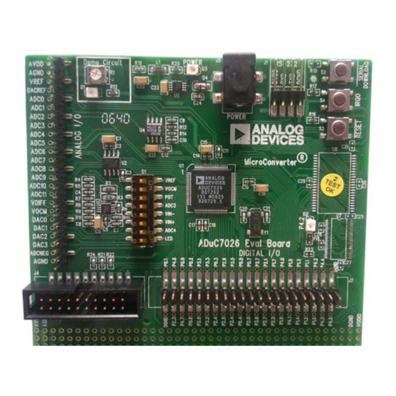
Figure 1. Typical Evaluation Board
Rev. B | Page 1 of 16
EVAL-ADuC7026 User Guide
MicroConverter
QUICKSTART PLUS DEVELOPMENT SYSTEM KIT
CONTENTS
ADuC7026
evaluation board
mIDAS-Link JTAG emulator
USB cable
Serial download cable
International power supply
CD containing
evaluation software
ADuC7026
data sheet
example code
GENERAL DESCRIPTION
This user guide, which replaces AN-744, refers to revision B2
of the
ADuC7026
MicroConverter® evaluation boards. Two
models of the development kit are available:
is the QuickStart™ Development System;
is the QuickStart Plus Development System. All references in
this user guide to the physical orientation of components on the
evaluation board are made with respect to a component-side
view of the board with the prototype area appearing at the
bottom of the board. The evaluation board is laid out to
minimize coupling between the analog and digital sections of
the board. To this end, the ground plane is split with the analog
section on the left side and a digital plane on the right side of
the board. The regulated 3.3 V power supply is routed directly
to the digital section and is filtered before being routed into the
analog section of the board.
UG-669
EVAL-ADuC7026QSZ
EVAL-ADuC7026QSPZ
Advertisement
Table of Contents

Related Manuals for Analog Devices EVAL-ADuC7026


Summary of Contents for Analog Devices EVAL-ADuC7026
-
Page 1: Features
EVAL-ADuC7026 User Guide UG-669 One Technology Way • P.O. Box 9106 • Norwood, MA 02062-9106, U.S.A. • Tel: 781.329.4700 • Fax: 781.461.3113 • www.analog.com Evaluating the ADuC7026 MicroConverter FEATURES QUICKSTART PLUS DEVELOPMENT SYSTEM KIT CONTENTS Full featured evaluation system for the ADuC7026 2-layer PCB (4”... -
Page 2: Table Of Contents
UG-669 EVAL-ADuC7026 User Guide TABLE OF CONTENTS Features ....................1 S1-2 V ..................5 QuickStart Development System Kit Contents ......1 S1-3 POT ..................5 QuickStart Plus Development System Kit Contents ....1 S1-4 ADC3 ..................5 General Description ................. 1 S1-5 VIN− ..................5 Evaluation Board ................ -
Page 3: Getting Started With The Evaluation Hardware
EVAL-ADuC7026 User Guide UG-669 GETTING STARTED WITH THE EVALUATION HARDWARE POWER SUPPLY CRYSTAL CIRCUIT Connect the 9 V power supply via the 2.1 mm input power The board is fitted with a 32.768 kHz crystal, from which the socket (J5). The input connector is configured as a center on-chip PLL circuit can generate a 41.78 MHz clock. -
Page 4: Power Indicator/General-Purpose Leds
UG-669 EVAL-ADuC7026 User Guide POWER INDICATOR/GENERAL-PURPOSE LEDS DAC1 can be used to control the brightness of the LED D1, when connected via the S1 switch. A power LED (D3) is used to indicate that a sufficient supply is GENERAL-PURPOSE PROTOTYPE AREA available on the board. -
Page 5: Dip Switch Link Options
EVAL-ADuC7026 User Guide UG-669 DIP SWITCH LINK OPTIONS S1-1 V S1-5 VIN− Function Function Connects the output of the 2.5 V external reference (ADR291) Connects the −OUT pin of the single-ended to differential op to the V pin (Pin 68) of the ADuC7026. -
Page 6: External Connectors
UG-669 EVAL-ADuC7026 User Guide EXTERNAL CONNECTORS ANALOG I/O CONNECTOR J3 Table 2. Pin Functions for Analog I/O Connector J3 Connector J3 provides external connections for all ADC inputs, Pin No. Pin Description reference inputs and DAC outputs. The pinout of the connector J3-1 is shown in Table 2. - Page 7 EVAL-ADuC7026 User Guide UG-669 Table 3. Pin Functions for Digital I/O Connector J2 Pin No. Pin Description Pin No. Pin Description J2-1 DGND J2-22 P2.0 CONV /SOUT/PLAO[5] J2-2 P4.5 START AD13/PLAO[13] J2-23 P0.5 J2-3 P4.4 IRQ1/ADC /MS0/PLAO[2] BUSY AD12/PLAO[12] J2-24 P0.4...
-
Page 8: External Memory Interface
UG-669 EVAL-ADuC7026 User Guide EXTERNAL MEMORY INTERFACE A footprint for a 32 k × 16 SRAM, a 64 k × 16 flash, and a Note that you can use different versions of the CY7C1020CV33 16-bit D-latch are provided on board because address and data memory, with different access times. -
Page 9: Added Table 4 And Changes To Figure 2
EVAL-ADuC7026 User Guide UG-669 AD[0:15] AT29LV1024 VDDIO ADR[0:15] ADR0 ADR1 ADR2 ADR3 ADR4 ADR5 ADR6 ADR7 ADR8 ADR9 ADR10 AD10 ADR11 AD11 ADR12 AD12 ADR13 AD13 74LVT16373ADGG ADR14 AD14 ADR15 AD15 ADR0 ADR1 1Q1 5 ADR2 1Q2 6 ADR3 1Q3 8... -
Page 10: Potentiometer Demonstration Circuit
UG-669 EVAL-ADuC7026 User Guide POTENTIOMETER DEMONSTRATION CIRCUIT By using the sample code in pot.c located in the code example AV DD folder on the accompanying CD, the variation in the AV DD potentiometer resistance can be seen on the output LED. -
Page 11: Changes To Figure 4
EVAL-ADuC7026 User Guide UG-669 SCHEMATIC AND ARTWORK Figure 5. Evaluation Board Schematic Rev. B | Page 11 of 16... -
Page 12: Change To Figure 6
UG-669 EVAL-ADuC7026 User Guide Figure 6. Evaluation Board Silkscreen Rev. B | Page 12 of 16... -
Page 13: Changes To Table 5
EVAL-ADuC7026 User Guide UG-669 BILL OF MATERIALS Table 5. Component Part Description Order No. Mfg. ADuC7026 PCB-1 2-sided, surface-mount PCB Analog Devices Evaluation Board, Revision B2 PCB Standoff Standoff Stick-on mounting feet 148-922 Farnell ADuC7026 MicroConverter (80-lead LQFP) ADuC7026CP Analog Devices... - Page 14 UG-669 EVAL-ADuC7026 User Guide NOTES Rev. B | Page 14 of 16...
- Page 15 EVAL-ADuC7026 User Guide UG-669 NOTES Rev. B | Page 15 of 16...
- Page 16 By using the evaluation board discussed herein (together with any tools, components documentation or support materials, the “Evaluation Board”), you are agreeing to be bound by the terms and conditions set forth below (“Agreement”) unless you have purchased the Evaluation Board, in which case the Analog Devices Standard Terms and Conditions of Sale shall govern. Do not use the Evaluation Board until you have read and agreed to the Agreement.
Need help?
Do you have a question about the EVAL-ADuC7026 and is the answer not in the manual?
Questions and answers