Table of Contents
Advertisement
Quick Links
FEATURES
Socket for evaluating ADD8504, ADD8505, or
Sockets for implementing gamma resistors
External drive capability
Simulates panel behavior
Sockets for capacitive loads
Sockets for resistive loads
Breadboard area
PACKAGE CONTENTS
Data sheets
ADD8504/ADD8505/ADD8506
EVAL-ADD8504/ADD8505/ADD8506 evaluation
board data sheet
CD including
Electronic version of
ADD8504/ADD8505/ADD8506
sheet
Electronic version of EVAL-ADD8505/ADD8505/ADD8506
evaluation board data sheet
Excel®-based spreadsheet for resistor and power
calculations
Five
ADD8504
devices
Five
ADD8505
devices
Five
ADD8506
devices
Rev. 0
Information furnished by Analog Devices is believed to be accurate and reliable. However, no
responsibility is assumed by Analog Devices for its use, nor for any infringements of patents or other
rights of third parties that may result from its use. Specifications subject to change without notice. No
license is granted by implication or otherwise under any patent or patent rights of Analog Devices.
Trademarks and registered trademarks are the property of their respective owners.
Evaluation Board for 4-, 5-, 6-Channel, Muxed
Input Line Inversion LCD Gamma Buffers
ADD8506
data sheet
data
EVALUATION BOARD
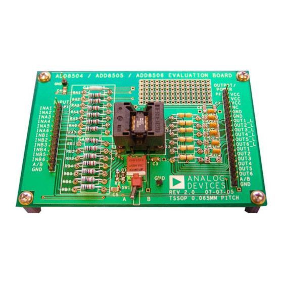
Figure 1. ADD8504/ADD8505/ADD8506 Evaluation Board
EVAL-ADD8504/ADD8505/ADD8506
GENERAL DESCRIPTION
The ADD8504/ADD8505/ADD8506 evaluation board
simplifies evaluation of the
under various conditions. This evaluation kit includes a gamma
voltage calculator, labeled ADD8504-05-06 Gamma Voltage
Calculator.xls, on the ADD8504/ADD8505/ADD8506
evaluation board kit CD to assist in determining required
external components to implement the desired gamma voltages.
This documentation is for the ADD8504/ADD8505/ADD8506
evaluation board only; for specific information regarding the
ADD8504/ADD8505/ADD8506
LCD gamma buffers, please refer to the datasheet.
One Technology Way, P.O. Box 9106, Norwood, MA 02062-9106, U.S.A.
Tel: 781.329.4700
Fax: 781.461.3113
ADD8504/ADD8505/ADD8506
muxed input line inversion
www.analog.com
©2006 Analog Devices, Inc. All rights reserved.
Advertisement
Table of Contents

Related Manuals for Analog Devices EVAL-ADD8504


Summary of Contents for Analog Devices EVAL-ADD8504
-
Page 1: Features
Information furnished by Analog Devices is believed to be accurate and reliable. However, no responsibility is assumed by Analog Devices for its use, nor for any infringements of patents or other One Technology Way, P.O. Box 9106, Norwood, MA 02062-9106, U.S.A. -
Page 2: Table Of Contents
EVAL-ADD8504/ADD8505/ADD8506 TABLE OF CONTENTS Features ....................1 Gamma Resistor Strings ...............4 Package Contents................1 Output Load Sockets..............4 General Description ................. 1 Evaluation Board Layout ..............5 Evaluation Board ................1 Functional Blocks................5 Revision History ................2 Evaluation Board Layers...............6 Setting Up the Evaluation Board ............ 3 Evaluation Board Schematic and Components......7... -
Page 3: Setting Up The Evaluation Board
EVAL-ADD8504/ADD8505/ADD8506 SETTING UP THE EVALUATION BOARD ADD8506 To begin using the ADD8504/ADD8505/ADD8506 evaluation board: The ADD8506 fills the socket and uses all input/output pins of the evaluation board. Use existing, or modify, Gamma Resistor RA1 to Gamma Resistor RA7, and Gamma Resistor RB1 to Gamma... -
Page 4: Switching
EVAL-ADD8504/ADD8505/ADD8506 SWITCHING The ADD8504/ADD8505/ADD8506 evaluation board can be INA1 switched by driving the A/B pin of Block 1 with a 0 V to 5 V INA2 clock. A 5 V input on the A/B pin selects GAMMA A; a 0 V INA3 input selects GAMMA B. -
Page 5: Evaluation Board Layout
EVAL-ADD8504/ADD8505/ADD8506 EVALUATION BOARD LAYOUT FUNCTIONAL BLOCKS BLOCK 6 BLOCK 2 BLOCK 3 BLOCK 4 Figure 4. Evaluation Board Layout Table 2. Evaluation Board Functional Block Descriptions Block Block Descriptions Block 1 Input and Monitoring Pins. Block 1 allows the user to force gamma voltages, drive Gamma Resistor Switch A/B, or monitor input voltages. -
Page 6: Evaluation Board Layers
EVAL-ADD8504/ADD8505/ADD8506 EVALUATION BOARD LAYERS Figure 5. Evaluation Board Layout—Top Layer Figure 6. Evaluation Board Layout—Bottom Layer Table 3. Evaluation Board Layer Descriptions Layer Description Blue (Top) Top-of-board metal traces and ground plane. See Figure 5. Red (Bottom) Bottom-of-board metal traces and ground plane. (Note: Top-view shown in Figure 6. Silk screen text is shown for orientation purposes;... -
Page 7: Evaluation Board Schematic And Components
EVAL-ADD8504/ADD8505/ADD8506 EVALUATION BOARD SCHEMATIC AND COMPONENTS Figure 7. Evaluation Board Schematic Rev. 0 | Page 7 of 8... -
Page 8: Ordering Guide
ESD protection circuitry, permanent damage may occur on devices subjected to high energy electrostatic discharges. Therefore, proper ESD precautions are recommended to avoid performance degradation or loss of functionality. ©2006 Analog Devices, Inc. All rights reserved. Trademarks and registered trademarks are the property of their respective owners. EB05763-0-2/06(0)
Need help?
Do you have a question about the EVAL-ADD8504 and is the answer not in the manual?
Questions and answers