
Related Manuals for Avnet PicoZed FMC V2


Summary of Contents for Avnet PicoZed FMC V2
- Page 1 PicoZed FMC Carrier Card PZCC-FMC-V2, Revision 1.1 Hardware User Guide Version 1.1 22 Sept 2016 v1.1...
-
Page 2: Table Of Contents
Table of Contents Introduction ........................3 Glossary ..........................3 Additional Documentation ....................3 PZCC-FMC-V2 Features: ......................4 Functional Description ..................... 8 Reset sources ........................8 User I/O – Switches and LEDs ....................9 I2C Address space and registers ..................11 Clocks ..........................12 PCIe x1 Gen2 Interface ......................13 FMC LPC Connector ...................... -
Page 3: Introduction
The PicoZed FMC Carrier Card Version 2 (PZCC-FMC-V2) is a development board designed for customers to easily evaluate the Avnet PicoZed System On Module (SOM) boards. This board provides an I/O breakout platform for the PicoZed SOMs. The PZCC-FMC-V2 provides all necessary SOM power, reset control and SoC I/O pin accessibility through the JX1, JX2, and JX3 MicroHeaders. -
Page 4: Pzcc-Fmc-V2 Features
1.3 PZCC-FMC-V2 Features: • Interfaces: FMC LPC (72 differential, 3 single ended) JTAG Single JTAG connector allows accesses to the Zynq and the FMC board through • automatic switching circuit. 4 Digilent Pmod™ compatible interfaces: • JPS1 connected to PS MIO •... - Page 5 • Power On Board ADP2384 single channel SMPS IC: • • Generates the primary board 5V power supply. 5V @ 4 Amp capable. ADP5052 five channel SMPS IC: • • VADJ: 1.8V, 2.5V, 3.3V up to 4A (user selectable voltage) •...
- Page 6 Figure 2 – PZCC-FMC-V2 Functional Block Diagram 22 Sept 2016 v1.1...
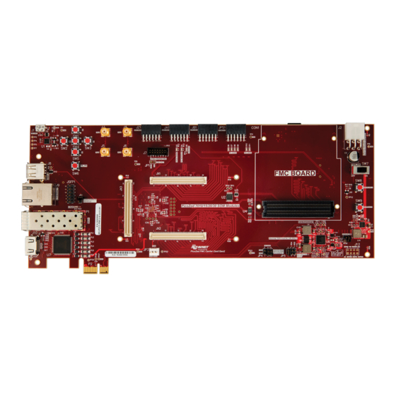
- Page 7 Figure 3 – PZCC-FMC-V2 Component Overview 22 Sept 2016 v1.1...
-
Page 8: Functional Description
The PZCC-FMC-V2 Carrier is an expansion board for the PicoZed SOMs. The primary I/O interface is via the LPC FMC connector. The board features additional MGT lanes for PCIe and SFP+. The PZCC-FMC-V2 bridges Avnet’s PicoZed SOM products to common high speed interfaces. -
Page 9: User I/O - Switches And Leds
2.2 User I/O – Switches and LEDs User Push Buttons: SW1 – SW6: 7015/20/30 SOM When a 7015/20/30 SOM is plugged in, the carrier provides 5 PL and 1 PS user GPIO push buttons for the Zynq-7000 AP SoC (blue and green in the table below). When a 7010 SOM is attached, only two switches are available - SW1 (PL_PB1) and SW6 (PS_PB1). - Page 10 User LEDs The Carrier has 6 SOM driven user LEDs – 4 PL and 2 PS. LEDs listed in green are available to the 7010 SOM. All LEDs (highlighted green and blue) are available to all other SOMs. A logic high from the Zynq-7000 AP SoC I/O turns the LED on.
-
Page 11: I2C Address Space And Registers
----------------------------------- | 1 | 1 | 1 | 1 | 1 | 0 | 0 | R/W | ----------------------------------- (When configured with Avnet factory default EEPROM config) 0xD8 ----------------------------------- | 1 | 1 | 0 | 1 | 1 | 0 | 0 | R/W |... -
Page 12: Clocks
2.4 Clocks Clock synthesizer IC - U13 IDT-242 I2C ADDR: 0xD8 The FMC2 contains an IDT 8T49N242-006 I2C programmable clock synthesizer to offer maximum clocking flexibility. Upon power up the part is configured via U14, a 24AA025T EEPROM. A 38.888MHz crystal is used for the synthesizer’s input for optimum performance and frequency selection. -
Page 13: Pcie X1 Gen2 Interface
SOM Net Name: Carrier Net Name: JX3 Pin: RSVD_PCIE_REFCLK0_P MGTREFCLK0_P RSVD_PCIE_REFCLK0_N MGTREFCLK0_N RSVD_MGTREFCLK1_P MGTREFCLK1_P RSVD_MGTREFCLK1_N MGTREFCLK1_N BANK13_LVDS_7_P PL_CLK Table 6 – Clock synthesizer pin table I2C Clock Configuration EEPROM – U14 EEPROM I2C ADDR: 0xA0 The clock configuration EEPROM is a Microchip 24AA025T-I/OT and is used to configure U13 when powered up. -
Page 14: Fmc Lpc Connector
• The PRSNT signals are used to identify the lane width (x1) of the PCIe bus for the host motherboard. The carrier ties the PRSNT1# and PRSNT2# signals together to accomplish this. The host motherboard has pull-up and pull-down resistors on these signals so the carrier does not require any other special configurations to enumerate as a single lane PCIe device when plugged into a host PC. - Page 15 The following guidelines have been observed in the layout of the FMC interface: CLK_#_M2C – 50 ohm single-ended impedance – Less than 10mil skew in P/N pair – Connected to MRCC (Multi-Region) – No length matching to any other feature ...
- Page 16 MicroHeader FMC LPC Connector LA[2:16]_<P|N> MRCC CLK0_M2C_<P|N> MRCC LA00_<P|N>_CC LA01_<P|N>_CC SRCC VREF_A_M2C Not Connected VADJ VADJ GBTCLK0_M2C_<P|N> Not Connected DP0_M2C_<P|N> Not Connected DP0_C2M_<P|N> Not Connected Jumpers GA[0:1] LA[19:33]_<P|N> MRCC CLK1_M2C_<P|N> LA17_<P|N>_CC MRCC LA18_<P|N>_CC SRCC PRSNT_L Not Connected VREF_A_M2C VADJ VADJ 3P3V AUX 3P3V 12P0V...
-
Page 17: Sfp+ Interface - P1 (7015/30 Som Only)
SFP+ Interface – P1 (7015/30 SOM only) The SFP+ interface is available to the 7015/30 SOM. The non-transceiver portion of the SFP+ interface is routed out to a vertical 0.1” connector (JSFP1). The SFP+ interface can be used without JSFP1 as long as the SFP+ doesn’t require control signals. If the SFP+ does require control signals, a loopback cable must be installed into JSFP1 and attached to the JZ PL PMOD connector. -
Page 18: Ps/Pl Pmod™ Interfaces - Ja, Jb, Jz & Jps1
PS/PL PMOD™ Interfaces – JA, JB, JZ & JPS1 The carrier has four Digilent Pmod™ right angle 0.1” female sockets (2x6). Three connectors are for the SoC’s PL (JA, JB, JZ) and one for the SoC’s PS (JPS1). These connections include eight GPIO. -
Page 19: Jx1, Jx2 And Jx3 Som Interface Microheaders
SOM Net Carrier JPS1 PMOD Pin Pmod™ Name: Net Name: Connection: Number: MIO13 PSPMOD_D0 MIO10 PSPMOD_D1 MIO11 PSPMOD_D2 MIO12 PSPMOD_D3 JPS1 MIO0 PSPMOD_D4 MIO9 PSPMOD_D5 MIO14 PSPMOD_D6 MIO15 PSPMOD_D7 Table 10 – JPS1 PS PMOD Pin Assignments JX1, JX2 and JX3 SOM Interface MicroHeaders The PicoZed Carrier has three 100-pin MicroHeaders (FCI, 61083-101400LF) for connection to the SOM. - Page 20 Table 11 – MicroHeader JX1 and JX2 Overview MicroHeader #1 (JX1) MicroHeader #2 (JX2) Signal Name Source Pins Signal Name Source Pins JX1 I/Os, for 7010/20: PUDC on JX1.17 (pulled JX2 I/Os for up to VCCO_34), Zynq Bank 34 7015/30: PUDC is Zynq Bank 35 PL_LED, PL_PB, on JX2.23.
- Page 21 Table 12 – MicroHeader JX3 Overview MicroHeader #3 (JX3) Signal Name Source Pin Count Bank 13 I/Os, PMODs JB & JZ, Zynq Bank 13 PL_CLK MGTTX I/Os Zynq Bank 112 MGTRX I/Os Zynq Bank 112 MGTREFCLK I/Os Zynq Bank 112 SD_CARD Zynq Bank 501 USB_UART...
-
Page 22: Multi-Gigabit Transceivers (Mgts)
2.10 Multi-Gigabit Transceivers (MGTs) Four MGT interfaces are available with the 7015/30 SOMs: 1) LPC FMC – see section: 2) PCIe x1 – see section: 3) SFP+ - see section: 4) 4 SMAs – see section: 2.10.1 • The PicoZed 7015 and 7030 SOMs have four multi-gigabit full-duplex transceiver lanes that reside on Bank 112 of the Zynq device. -
Page 23: Usb Uart - J1
The PZCC-FMC-V2 has four MGT Data SMA Female connectors for differential TX_P/N and RX_P/N data connections. These I/O’s are not DC blocked on the carrier. If DC blocking is required for your application, Avnet recommends using an inline capacitor, such as the Fairview part: http://www.fairviewmicrowave.com/inner-dc-block-5-mhz-18-ghz-sma-connectors-sd3241-p.aspx... -
Page 24: Usb Otg Interface - J8
2.12 USB OTG Interface – J8 A USB Type A connector is routed to the SOM via header JX3 pins 63, 67, 69 and 70. In USB OTG Host mode (default), this interface sources VIN_HDR (+5.0V) power onto the USB_VBUS rail via power switch (U10) when an active high control signal is present on USB_OTG_CPEN (JX3.70). -
Page 25: Som 10/100/1000 Ethernet Rj45 - J9
2.13 SOM 10/100/1000 Ethernet RJ45 – J9 J9 is a SOM direct connect Ethernet port. The connector is a MagJack L829-1J1T-43 and contains integrated magnetics and two LEDs for connection indication. The left side LED[1] is green and indicates link status while the right side LED[0] is amber and indicates link activity. Figure 12 –... -
Page 26: Mac Id - Eeprom
2.14 MAC ID – EEPROM MAC ID I2C ADDR: 0xA2 The SOM does not contain a MAC ID EEPROM so the carrier has one placed for design flexibility. A 2Kb MAC ID EEPROM with EUI-48 Node Identity (Microchip PN: 24AA025E48) is used to store the MAC ID for the SOM’s Ethernet PHY. -
Page 27: Mac Id - Uni/O Eeprom (7Z015/30 Only)
2.15 MAC ID – UNI/O EEPROM (7Z015/30 only) In addition to the MAC ID EEPROM, a second 2Kb MAC ID UNI/O® EEPROM with EUI-48 Node Identity (Microchip PN: 11AA02E48) is used to store a MAC address for a SFP+ Ethernet module. - Page 28 RTC Battery installation instructions: The CR1025 battery is required to be installed in a sleeve, part number BHX1-1025 (included in PZCC-FMC-V2 KIT) and firmly inserted into the carrier’s socket. The coin cell’s positive terminal is placed into the opening of the sleeve facing up. Please see figures below: Figure 16 –...
-
Page 29: Hdmi Interface - J10
2.17 HDMI Interface – J10 The PZCC-FMC-V2 has a HDMI V1.4 and DVI V1.0 video output port, J10. The data is configured for the YCbCr 4:2:2 format. This port is based on the Analog Devices ADV7511 225MHz HDMI transmitter IC, capable of transmitting up to 1080p resolution video. The port is a 16 bit interface, using data signals ADV7511 D20 to D35 and is split across the JX1 and JX2 interfaces. -
Page 30: Microsd Card Interface
4 card or better is recommended. Up to 32 GB is supported. If a user intends to use the microSD card interface at industrial temperatures, an industrial temperature microSD card is required. Please request more information on this from your local Avnet representative. Alternatively, the customer can load their image on the eMMC memory on the SOM. -
Page 31: Fan Header - Jp3
2.19 Fan Header – JP3 JP3, a three pin 0.85” pitch fan header has been placed to allow the customer to use a fan for SOM cooling if needed. By default the header is connected to the VIN_SW which is +12V via R161. -
Page 32: Power
The maximum input current from J2 is limited by filter L11, which has a rating of 5.0 Amps. Any current exceeding this value will damage the filter network. The power supply shipped from Avnet is Avnet part number AES-SLP-12V5A-G and is rated at 12V, 5.0 Amps and is recommended for use with the PZCC-FMC-V2 board. -
Page 33: Molex To Non-Atx Connection
If this placement is undesirable, the capacitor may be removed by the customer after power testing has been performed with it removed. Avnet has not tested power performance with this component removed. Functional area... -
Page 34: Jp1 - Fpga Vbat (Vccbatt)
3.5 JP1 – FPGA VBAT (VCCBATT) JP1 is a non-populated 100 mil dual pin connector. Use this connection to provide battery backup power for the FGPA’s internal volatile memory that stores the key for the AES decryptor. If using this connection, the SOM will require a resistor to be removed. Please see the appropriate SOMs User Guide (choose the latest revision): http://picozed.org/support/documentation/4736 NOTE: The voltage input to this connector MUST NOT EXCEED 2.0V or FPGA damage may... -
Page 35: Sequencing
3.7 Sequencing • PWR_EN signal, active high, JX1.5, allows the carrier to turn on or off the PicoZed power supplies. R18 and C6 have been placed to adjust the timing of this signal during power off conditions. This signal should not be de-asserted until VCCIO_EN is de- asserted. -
Page 36: Bypassing/Decoupling/Filtering
3.8 Bypassing/Decoupling/Filtering The PZCC-FMC-V2 follows the recommended decoupling and layout techniques per each manufacturer’s datasheet. 3.9 PG Module Power Good LED A green status LED, D4, illuminates when PG_CARRIER signal is high (good). Figure 24 – PG_MODULE LED 22 Sept 2016 v1.1... -
Page 37: Jumpers, Configuration And Test Points
4 Jumpers, configuration and test points: The below table is a quick reference to all of the jumpers, configuration settings and test points on the FMC. For detailed information, refer to the appropriate sections in this document. Reference Name Default Notes: Designator Attach a 1.5V battery to this connection to maintain FPGA... -
Page 38: Fmc Ga [1:0] Jumper Header
4.1 FMC GA [1:0] jumper header The carrier allows the user to select the FMC board address via JP4 and 2 jumper headers. The address range is from 0 to 3 via jumper headers. The jumpers force a high or a low on address bits 1 or 0. -
Page 39: Power Supply Monitor Header - J12
4.3 Power Supply monitor header – J12 The PZCC-FMC-V2 has a power supply monitor connection. While this is primarily for testing, it can be accessed by the user to monitor the voltages on the carrier card. The below figure shows the available voltage monitor points. Figure 27 –... -
Page 40: Revision History
6 Revision History Version date Ver # Reason for change 26 Apr 2016 Initial release Table 23 – Revision History 22 Sept 2016 v1.1... -
Page 41: Appendix A - Additional Information/Test Results
For NON-Standard protocols, Avnet recommends using 5.0Gbps as a max data rate, as this is the most stable link with greatest margin across the largest set of bit streams. More performance may be obtained by adjusting the speed up or down as necessary. - Page 42 PicoZed SOMs at the industrial temperature range (-40C to +85C). This testing was performed to validate the SOMs operating range and not the carrier’s, therefore the carrier is not guaranteed to operate at this range yet Avnet has not had a failure in doing so. III. EMI Compliance: There is no requirement for the PZCC-FMC-V2 to be tested to meet emissions compliance.
Need help?
Do you have a question about the PicoZed FMC V2 and is the answer not in the manual?
Questions and answers