Avnet Ultra96-V2 Hardware User's Manual
Hide thumbs
Also See for Ultra96-V2:
- Getting started manual (33 pages) ,
- Getting started manual (44 pages) ,
- Manual (15 pages)
Table of Contents
Advertisement
Advertisement
Table of Contents

Subscribe to Our Youtube Channel
Related Manuals for Avnet Ultra96-V2


Summary of Contents for Avnet Ultra96-V2
- Page 1 Ultra96-V2 Hardware User’s Guide Revision 1 Version 1.0 Page 1 Copyright © 2019 Avnet, Inc. AVNET, “Reach Further,” and the AV logo are registered trademarks of Avnet, Inc. All other brands are the property of their respective owners. LIT# Ultra96-V2-HW-User-Guide-rev-1-0-V1...
-
Page 2: Table Of Contents
Document Control ....................3 Version History ...................... 3 Introduction ......................3 Glossary ........................... 5 Reference Documents ......................5 Ultra96-V2 Architecture and Features ..............6 List of Features ........................6 Ultra96-V2 Block Diagram ....................... 7 Functional Description ................... 8 Zynq UltraScale+ MPSoC ......................8 5.1.1... -
Page 3: Document Control
Date Comment 23 May 2019 Initial Release 3 Introduction The main purposes of the Ultra96-V2 Kit are: Provide a Xilinx entry in the 96Boards community • • Combine ARM processing with programmable logic in a convenient and expandable board •... - Page 4 Embedded Computing Robotics Wireless design and demonstrations using Wi-Fi and Bluetooth Page 4...
-
Page 5: Glossary
Glossary Term Definition Zynq UltraScale+ MPSoC Processing System Zynq UltraScale+ MPSoC Programmable Logic PS Multiplexed Input Output Pins Power On Reset Application Processing Unit Real-time Processing Unit Graphics Processing Unit SYSMON System Monitor High Density PL I/O Pins High Performance PL I/O Pins PMBus Power Management Bus Reference Documents... -
Page 6: Ultra96-V2 Architecture And Features
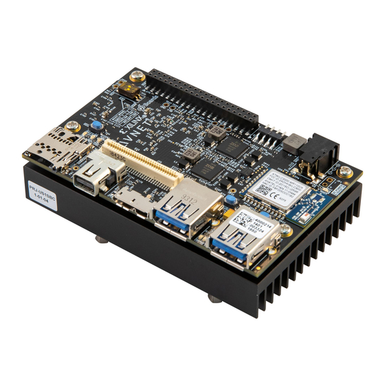
4 Ultra96-V2 Architecture and Features This section summarizes the features of the development board, followed by functional descriptions of each circuit. List of Features The Ultra96-V2 Developer Kit supports the following features: • Zynq UltraScale+ MPSoC ZU3EG SBVA484 • Storage... -
Page 7: Ultra96-V2 Block Diagram
Ultra96-V2 Block Diagram Figure 1 – Ultra96-V2 Block Diagram Page 7... -
Page 8: Functional Description
5 Functional Description The following sections provide brief descriptions of each feature provided on the Ultra96-V2 board. Zynq UltraScale+ MPSoC The Zynq UltraScale+ MPSoC ZU3EG device (in the SBVA484 package) contains: • Processor System (PS): Application Processing Unit Quad-core ARM Cortex-A53 MPCore with CoreSight; NEON & Single/Double Precision Floating Point;... -
Page 9: Sbva484 Package
5.1.1 SBVA484 Package Figure 2 – SBVA484 Package Diagram Page 9... -
Page 10: Pl I/Os (Banks 26, 65, 66)
ZU3EG provides one HD bank (Bank 26) with 24 pins, one HP bank (Bank 65) with 52 pins, and another HP bank (Bank 66) with 6 pins. The PL I/Os on Ultra96-V2 are tied to the Low-Speed 96Boards Mezzanine, the High-Speed 96Boards Mezzanine, Bluetooth, and the fan. - Page 11 Table 2 – PL IO Bank 65 MPSoC Pin Number Bank MPSoC Site Name Function FAN_PWM CSI0_C_N Expansion CSI0_C_P CSI0_D0_N CSI0_D0_P CSI0_D1_N CSI0_D1_P CSI0_D2_N CSI0_D2_P CSI0_D3_N CSI0_D3_P CSI1_C_N CSI1_C_P CSI1_D0_N CSI1_D0_P CSI1_D1_N CSI1_D1_P DSI_CLK_N DSI_CLK_P DSI_D0_N DSI_D0_P DSI_D1_N DSI_D1_P DSI_D2_N DSI_D2_P DSI_D3_N DSI_D3_P...
- Page 12 NetR35_1 Table 3 – PL IO Bank 66 MPSoC Pin Bank MPSoC Site Name Function Number HSIC_STR HS Expansion MIO7_Radio_RST_N Radio Page 12...
-
Page 13: Ps Mios (Banks 500, 501, 502)
5.1.3 PS MIOs (Banks 500, 501, 502) Table 4 – MIO Overview Bank 500 1.80V UART1 UART0 I2C1 SPI1 SPI1 WE BE PB SD0 USB Bank 501 1.80V DPAUX PMIC SPI0 PK TP SPI0 Bank 502 1.80V USB0 USB1 UART1 - Header UART0 - Bluetooth (+ PL RTS/CTS) I2C1 - I2C Hub SPI1 - HS Expansion Header... - Page 14 Table 5 – MIO Bank 500 (MIOs 0 to 25) Bank Pin # Device Signal Notes 0 UART1 MIO0_UART1_TX UART Header J1 MIO1_UART1_RX 2 UART0 MIO2_UART0_RX_BT_HCI_TX ATWILC300 MIO3_UART0_TX_BT_HCI_RX 4 I2C1 MIO4_I2C1_SCL I2C Mux MIO5_I2C1_SDA 6 SPI1 MIO6_SPI1_SCLK Hi-speed Expansion Header 7 GPIO MIO7_RRAD_RST_N ATWILC300 Reset...
- Page 15 Table 6 – MIO Bank 501 (MIOs 26 to 51) Bank Pin # Device Signal Notes 26 GPIO MIO26_PWR_INT Pushbutton On/Off Controller Interrupt, Pushbutton turn-off event detected 27 DPAUX MIO27_DP_AUX_OUT DPAUX single-ended output MIO28_DP_HPD DPAUX Hot Plug Detect MIO29_DP_OE DPAUX Output Enable MIO30_DP_AUX_IN DPAUX single-ended input 31 GPIO...
- Page 16 Table 7 – MIO Bank 502 (MIOs 52 to 77) Bank Pin # Device Signal Notes 52 USB0 MIO52_USB0_CLK USB0 Clock MIO53_USB0_DIR USB0 Data bus direction MIO54_USB0_DATA2 USB0 Data 2 MIO55_USB0_NXT USB0 Data flow MIO56_USB0_DATA0 USB0 Data 0 MIO57_USB0_DATA1 USB0 Data 1 MIO58_USB0_STP USB0 Stop transfer MIO59_USB0_DATA3...
-
Page 17: Ps Bank 503
5.1.4 PS Bank 503 Mode, config, PSJTAG, error, SRST, and POR. Bank 503 contains system-level pins, including Table 8 – PS Bank 503 MPSoC Pin Bank MPSoC Site Name Number PS_ERROR_OUT PS_ERROR_STATUS PS_INIT_N PS_MODE0 PS_MODE1 PS_MODE2 PS_MODE3 PS_PAD_IN PS_PAD_OUT POWER_GOOD PS_REF_CLK PS_SRST_N Page 17... -
Page 18: Ps Bank 504
5.1.5 PS Bank 504 Bank 504 contains the DDR Controller pins which are connected to LPDDR4 on Ultra96-V2. Table 9 – PS Bank 504 MPSoC Pin Bank MPSoC Site Name Number AA22 PS_DDR_CAA0 AB20 PS_DDR_CAA1 AB17 PS_DDR_CAA2 AB19 PS_DDR_CAA3 AB21... - Page 19 AA12 PS_DDR_DQ10 AB12 PS_DDR_DQ11 PS_DDR_DQ12 AA14 PS_DDR_DQ13 PS_DDR_DQ14 AB15 PS_DDR_DQ15 PS_DDR_DQ16 PS_DDR_DQ17 PS_DDR_DQ18 PS_DDR_DQ19 PS_DDR_DQ20 PS_DDR_DQ21 PS_DDR_DQ22 PS_DDR_DQ23 PS_DDR_DQ24 PS_DDR_DQ25 PS_DDR_DQ26 PS_DDR_DQ27 PS_DDR_DQ28 PS_DDR_DQ29 PS_DDR_DQ30 PS_DDR_DQ31 PS_DDR_DQSA0_C AA13 PS_DDR_DQSA1_C S_DDR_DQSB0_C PS_DDR_DQSA1_T PS_DDR_DQSA0_T PS_DDR_DQSA1_T PS_DDR_DQSB0_T PS_DDR_DQSB1_T PS_DDR_RST_N NetR23_2 Page 19...
-
Page 20: Ps Bank 505
5.1.6 PS Bank 505 Bank 505 contains the transceivers. Table 10 – PS Bank 505 MPSoC Pin Bank MPSoC Site Name Number U26M_N U26M_P U27M_N U27M_P GTR_LANE0_TX_N GTR_LANE0_TX_P GTR_LANE1_TX_N GTR_LANE1_TX_P GTR_LANE2_RX_N GTR_LANE2_RX_P GTR_LANE2_TX_N GTR_LANE2_TX_P GTR_LANE3_RX_N GTR_LANE3_RX_P GTR_LANE3_TX_N GTR_LANE3_TX_P NetR22_2 Page 20... -
Page 21: Lpddr4 Memory
MT53D512M32D 2DS-053 AIT:D. microSD Card Ultra96-V2 provides a microSD card socket as the primary boot device. VCCO for the SDIO lines going into the Zynq MPSoC is 1.80V thus a level shifter is required to go from the 3.3V native SD card slot to 1.80V... -
Page 22: Usb
Ultra96-V2 provides one upstream (device) and two downstream (host) USB 3.0 connections. A USB 2.0 downstream (host) interface is provided on the high speed expansion bus. Two Microchip USB3320 USB 2.0 ULPI Transceivers and one Microchip USB5744 4-Port SS/HS USB Controller Hub are specified. -
Page 23: Wi-Fi / Bluetooth
Ultra96-V2 supports one Mini DisplayPort output. A TE Connectivity 2129320-3 provides the Mini DisplayPort connectivity. UART Ultra96-V2 provides access to one UART on the baseboard. PS UART1 (MIO0, MIO1) is connected to a 4-pin 2mm header (J1). Table 12 – Pinout for the J1 UART Header... -
Page 24: User Leds
5.10 MPSoC Thermal Bracket with Fan The Ultra96-V2 uses a thermal bracket with a fan for the MPSoC device. The bracket is mounted to the bottom side of the Ultra96-V2 to help dissipate heat. The bracket also has additional mounting holes to allow for other possible thermal solutions. - Page 25 Table 13 – Low Speed Expansion Connector Ultra96 96Boards Pin # Pin # 96Boards Ultra96 HD_GPIO0 UART0_CTS PWR_BTN_N PWR_BTN_N HD_GPIO1 UART0_TxD RST_BTN_N RST_BTN_N HD_GPIO2 UART0_RxD SPI0_SCLK PS_MIO38 HD_GPIO3 UART0_RTS SPI0_DIN PS_MIO42 HD_GPIO4 UART1_TxD SPI0_CS PS_MIO41 HD_GPIO5 UART1_RxD SPI0_DOUT PS_MIO43 PS_I2C0_SCL I2C0_SCL PCM_FS HD_GPIO9...
-
Page 26: High Speed Expansion Connector
Amphenol FCI 61082-061409LF (or compatible) 60 pin low profile 0.8mm receptacle is specified. Table 14 shows the pinout of the High Speed Expansion Header (Ultra96-V2 column) and the differences from the 96Boards specification (96Boards column). With the exception of SD, I2C2 and I2C3, all dedicated interfaces specified by 96Boards are replaced with GPIO. -
Page 27: Configuration And Debug
6 Configuration and Debug Boot Mode Ultra96-V2 supports booting from JTAG and microSD Card. A DIP switch (SW3) is installed to allow selecting the desired boot mode. Figure 5 – Boot Mode Switch (SD Boot Mode Shown) JTAG Configuration and Debug JTAG access to the MPSoC is available through a 1x8 header (J3). -
Page 28: Power
EIAJ-3 compliant DC plug available up to 2A, which is 4.75 mm outer diameter with 1.7mm center pin (4.75/1.7), for the power supply https://en.wikipedia.org/wiki/EIAJ_connector • However, there is a bit of flexibility. Avnet offers a 12V supply as an accessory (part number: AES-ACC-U96-4APWR) with the following specifications: • Input: 100-240V, 50/60HZ •... -
Page 29: Power Regulators
Avnet has also provided an example of this spreadsheet filled out for the Ultra96-V2 under Documentation on the Ultra96-V2 website. Power Regulators A configurable multi-rail PMIC provides all power for the Ultra96-V2. The power rail configuration is shown below: Figure 8 –... -
Page 30: Power Sequence
Power Sequence Here we have the defined power up sequencing for the Ultra96-V2. Figure 9 – Power up Sequencing The captures below show the power up sequencing measurements taken on the Ultra96-V2: Pink – 5V Yellow – VCCPSINT_LP Yellow – VCCPSINT_LP... - Page 31 Yellow – VCCPSINT_LP Blue – VCCPSINT_FP Dark Blue – VCCINT Light Blue – VCCPSAUX Pink – VCCINT Light Blue – VCCPSAUX Dark Blue – VCCO PSDDR 1.1V Pink – VCCAUX Yellow – VCCPSINT_LP Yellow – VCCPSINT_LP Light Blue – VCCAUX Pink –...
-
Page 32: Clocks
These clocks are generated by the IDT 5P49V6975 programmable clock generator. 9 Reset Ultra96-V2 Reset is managed by the Infineon PMICs. At power-up, the ZU3EG is held in reset until all power rails have ramped up and are stable. A pushbutton allows manually resetting the ZU3EG.
Need help?
Do you have a question about the Ultra96-V2 and is the answer not in the manual?
Questions and answers