
Related Manuals for Avnet MicroZed


Summary of Contents for Avnet MicroZed
- Page 1 MicroZed I/O Carrier Card Zynq™ System On Module Hardware User Guide Revision 1.1 30 Oct 2020...
-
Page 2: Table Of Contents
2.4.3 DIP Switches ........................8 ........................9 NTERFACE EADERS 2.5.1 Digilent Pmod™ Compatible Expansion Headers (2x6) ............9 2.5.2 JX1 and JX2 MicroZed interface microheaders ..............13 (AMS) I ................19 GILE IXED IGNALING NTERFACE 2.6.1 XADC alternate GPIO function ..................20 JTAG C ...................... -
Page 3: Introduction
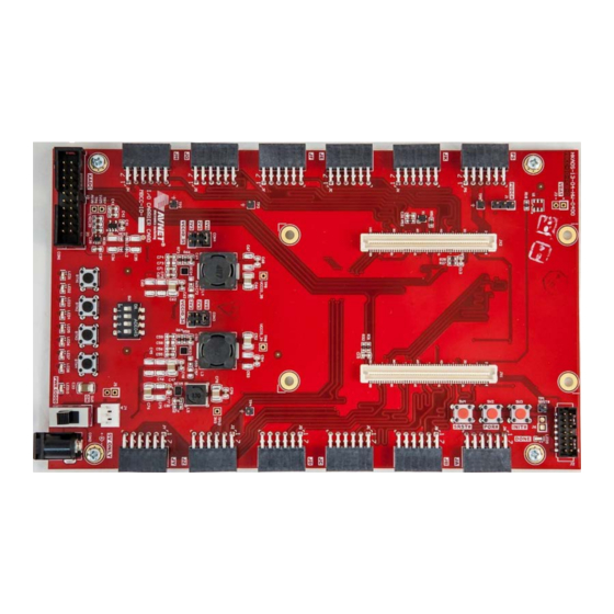
1 Introduction The MicroZed I/O Carrier Card (IOCC) is a low cost evaluation board for the MicroZed series System On Module (SOM) boards. The function of this board is to provide SoC I/O pin accessibility to the MicroZed SOM board through the 12 PMOD connectors. In addition to SoC I/O pin access through the PMOD connectors, the IOCC also provides SOM board power via the JX MicroHeaders. - Page 4 4 DIP Switches 4 Pushbuttons BTN /32 / 8 /7** 6 Pmod ** Bank 13 Pmod only has 7 I/O Pins - 4 Bank 35 - 1 Bank 13 - PS Pmod Figure 1 – MicroZed IOCC Block Diagram 30-Oct-2020, Rev. 1.1...
- Page 5 Figure 2: IOCC Topology 30-Oct-2020, Rev. 1.1...
-
Page 6: Zynq Bank Pin Assignments
1.1 Zynq Bank Pin Assignments The following figure shows the Zynq bank pin assignments on the MicroZed followed by a table that shows the detailed I/O connections. See tables Table 12 – JX1 Connections and Table 13 – JX2 Connections. -
Page 7: Functional Description
Functional Description The I/O Expansion Carrier Card is an expansion board for Avnet’s MicroZed 7Z010 or 7Z020 System On Module (SOM) product. It adds up to 12 Digilent Pmod™ compatible Interfaces, 8 User LEDs, 4 User Pushbuttons, 4 DIP Switches and a Xilinx analog interface. -
Page 8: Power On Reset - Por# Button - Sw2
MicroHeader. When asserted, this signal resets the USB UART, USB OTG circuit and turns off the IOCC VCCIO_34/35 power supplies. It is used to invoke an IOCC and MicroZed total system power reset. The PS and PL are reset to power on default settings and the selected boot process is initiated. -
Page 9: User I/O
User I/O 2.4.1 User Push Buttons The Carrier provides 4 user GPIO push buttons to the Zynq-7000 AP SoC.. Pull-down resistors provide a known low default state. Pushing a button connects to VCCio_35 to assert a logic high. Table 6 – Push Button Connections Carrier MicroHeader Zynq AP SOC... -
Page 10: Interface Headers
The PS Pmod is 3.3V only. • 7Z020 MicroZed only: Pmods™ ,JY and JZ, are sourced by Bank 13 and thus only available when MicroZed is populated with a 7Z020 device. Pmod™ JZ only has 7 pin connections, thus this Pmod™ interface cannot interface to QSPI or SD interface per the Digilent Pmod™... - Page 11 Figure 4 – Digilent Compatible Pmod™ Interface Layout FPGA I/O FPGA I/O FPGA I/O FPGA I/O 3.3V FPGA I/O FPGA I/O FPGA I/O FPGA I/O 3.3V Figure 5 – Digilent Pmod™ Compatible Interface Connections when VCCIO_34/35 set to 3.3V. Table 9 – Digilent Pmod™ Compatible Interface Connections Carrier Pmod Pin MicroHeader...
- Page 12 Carrier Pmod Pin MicroHeader Zynq AP SOC Pmod™ Net Name Number Connection Connection JD0-1 P Pin 1 JX1, pin 67 Bank 34, R16 JD0-1 N Pin 2 JX1, pin 69 Bank 34,R17 JD2-3 P Pin 3 JX1, pin 68 Bank 34, T17 JD2-3 N Pin 4 JX1, pin 70...
- Page 13 JH6-7 P Pin 9 JX2, pin 82 Bank 35,L14 JH6-7 N Pin 10 JX2, pin 84 Bank 35,L15 Carrier Pmod Pin MicroHeader Zynq AP SOC Pmod™ Net Name Number Connection Connection JK0-1 P Pin 1 JX1, pin 61 Bank 34, Y18 JK0-1 N Pin 2 JX1, pin 63...
-
Page 14: Jx1 And Jx2 Microzed Interface Microheaders
JX1 and JX2 MicroZed interface microheaders The Carrier features two MicroHeaders (TE PN: 5177984-4) for connection to MicroZed. Each connector interfaces to Zynq PL I/O as well as eight PS-GPIO, six dedicated analog inputs, and four dedicated JTAG signals. *NOTE: the eight PS-GPIO and four JTAG signals are shared on MicroZed, thus for each interface, it can only be used on either MicroZed or the Carrier, not simultaneously. - Page 15 Table 10 – Bank 13 Pins Number of Pins Name Pin Number VCCO_13 IO_L6N_T0_VREF_13 IO_L12P_T1_MRCC_13 IO_L12N_T1_MRCC_13 IO_L11P_T1_SRCC_13 IO_L11N_T1_SRCC_13 IO_L15P_T2_DQS_13 IO_L15N_T2_DQS_13 IO_L19P_T3_13 IO_L19N_T3_VREF_13 IO_L20P_T3_13 IO_L20N_T3_13 (Byte Group T3) IO_L21P_T3_DQS_13 IO_L21N_T3_DQS_13 IO_L22P_T3_13 IO_L22N_T3_13 ** With only one pin for VCCO_13, the PCB trace must be able to carry 500mA. 2.5.2.1 MicroHeader pinout assignments: Table 11 –...
- Page 16 Table 12 – JX1 Connections Carrier Connection Carrier MicroHeader Zynq AP SOC Zynq AP SOC Pin Net Name Connection Connection XADC, pin 1 XADC_V_N JX1, pin 99 Bank 0, K9 VN_0 XADC, pin 2 XADC_V_P JX1, pin 97 Bank 0, L10 VP_0 XADC, pin 9 XADC-DX_P...
- Page 17 PUDC PUDC# JX1, pin 17 Bank 34, U13 IO_L3P_T0_DQS_PUDC_B_34 DONE_LED FPGA_DONE JX1, pin 8 Bank 0, R11 DONE_0 CARRIER_SRST# CARRIER_SRST# JX1, pin 6 PWR_EN PWR_EN JX1, pin 5 JTAG_TDO JTAG_TDO JX1, pin 3 Bank 0, F6 TDO_0 JTAG_TDI JTAG_TDI JX1, pin 4 Bank 0, G6 TDI_0 JTAG_TMS...
- Page 18 JG0-1 P IO_L15P_T2_DQS_AD12P_3 Pmod JG, pin 1 JX2, pin 62 Bank 35, F19 JG0-1 N Bank 35, F20 IO_L15N_T2_DQS_AD12N_ Pmod JG, pin 2 JX2, pin 64 Pmod JG, pin 3 JG2-3 P JX2, pin 61 Bank 35, G17 IO_L16P_T2_35 Pmod JG, pin 4 JG2-3 N JX2, pin 63 Bank 35, G18...
- Page 19 2.5.2.2 Layout Routing Guidelines • The signals for each header follow FMC routing tolerances and guidelines. Each of the P/N pairs have 50Ω single-ended impedance (100Ω differential) with less than 10 mil skew between all P/N pairs on each header. •...
-
Page 20: Agile Mixed Signaling (Ams) Interface
2.6 Agile Mixed Signaling (AMS) Interface The XADC header provides analog connectivity for analog reference designs, including AMS daughter cards such as Xilinx’s AMS Evaluation Card. Both analog and digital IO can be easily supported for a plug in card. The pin out has been chosen to provide tightly coupled differential analog pairs on the ribbon cable and to also provide AGND isolation between channels. -
Page 21: Xadc Alternate Gpio Function
2.6.1 XADC alternate GPIO function If the XADC function is not desired, the port can be used for additional GPIO expansion as necessary. However, care must be taken to ensure the appropriate logic voltage levels are observed when using these signals. VCCIO_35 sets the acceptable voltage levels for the XADC_GIOx signals. - Page 22 Table 16 – Analog Header Pin Out XADC Name Description Requirement Zynq Pin Header Two pins required. Dedicated 1V peak-to- pins on the 7 series package. peak input XADC-VN-R : M12 This is the dedicated analog maximum XADC-VP-R : L11 input channel for the ADC(s).
-
Page 23: Jtag Configuration
The Carrier provides a traditional Platform Cable JTAG connector for use with Xilinx Platform Cables and Digilent JTAG HS1 or HS2 Programming Cables. When a MicroZed is plugged onto the Carrier, the Carrier’s JTAG connector MUST be used. The JTAG connector on-board the MicroZed SOM will no longer function. -
Page 24: Power
CON2. The input voltage range is from 5V to 12 volts. The current rating of the power supply is determined by the total expected power consumption of the project. The default power supply sent by Avnet is a 5V, 2 Ampere power supply for general low power I/O applications and XADC header use. -
Page 25: Voltage Regulators
The following table lists the power solution for the IO Carrier Card. Two rails are independent and adjustable supplying power to the Zynq PL I/O banks and connected Pmods™. VCCio_35 drives banks 35 and 13 (if 7Z020 is populated on MicroZed) as well as 5 Pmod™ connectors. -
Page 26: Bypassing/Decoupling
VCCIO regulators. The VCCIO regulators are sequenced in series and cannot be enabled until Zynq’s core power is valid. The PG_CARRIER (on IOCC) and PG_MODULE (on MicroZed) signals are wired OR and tied to the Zynq Power On Reset signal. When the power supplies are valid on both the SOM and carrier, the PG signal de-asserts the Zynq POR signal. -
Page 27: Jumpers, Configuration And Test Points
Fan Header Not Populated Attached to Vin VCCIO_EN Not Populated Used to test the on-board power supplies without a MicroZed inserted. PG_CARRIER Not Populated Used to test the on-board power supplies without a MicroZed inserted. DIP_SW0-3 DIP_SWx In low position 4 user slide switches to the Zynq PL fabric. -
Page 28: Mechanical
3 Mechanical 3.1 Dimensions: Figure 10: IOCC Horizontal Mechanical Dimensions (mils) Figure 11 - Total height from Bumper to Switch top – 20.00 mm Figure 12 - Switch Height - no bumpers – 18.00 mm 30-Oct-2020, Rev. 1.1... -
Page 29: Weight
Figure 13 - bottom of PCB to top of JX.x connector – 6.40 mm 3.2 Weight: The weight of the IOCC with rubber feet and all jumpers populated is 110 grams/3.8801 oZ. 4 Revision History Rev date Rev # Reason for change Updated graphics and power section.
Need help?
Do you have a question about the MicroZed and is the answer not in the manual?
Questions and answers