Table of Contents
Advertisement
Quick Links
UM2592
User manual
STM32WL Nucleo-64 board (MB1389)
Introduction
The NUCLEO-WL55JC STM32WL Nucleo-64 board, based on the MB1389 reference board (NUCLEO-WL55JC1 and
NUCLEO-WL55JC2 order codes), provides an affordable and flexible way for users to try out new concepts and build prototypes
with the STM32WL Series microcontroller, choosing from the various combinations of performance, power consumption, and
features.
®
The ARDUINO
Uno V3 connectivity support and the ST morpho headers provide an easy means of expanding the functionality
of the STM32WL Nucleo open development platform with a wide choice of specialized shields.
The STM32WL Nucleo-64 board does not require any separate probe as it integrates the STLINK-V3E debugger and
programmer.
The STM32WL Nucleo-64 board is provided with the STM32WL comprehensive software HAL library and various packaged
software examples available with the STM32CubeWL MCU Package.
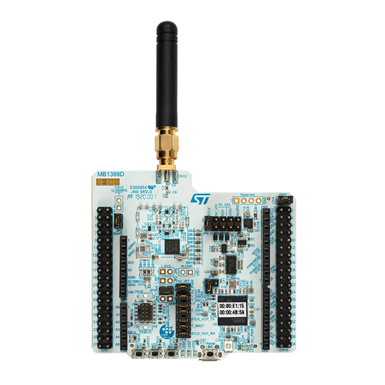
Figure 1.
NUCLEO-WL55JC top view
Figure 2.
NUCLEO-WL55JC bottom view
Pictures are not contractual.
UM2592 - Rev 1 - November 2020
www.st.com
For further information contact your local STMicroelectronics sales office.
Advertisement
Table of Contents

Related Manuals for ST NUCLEO-WL55JC STM32WL


Summary of Contents for ST NUCLEO-WL55JC STM32WL
-
Page 1: Figure 1. Nucleo-Wl55Jc Top View
® The ARDUINO Uno V3 connectivity support and the ST morpho headers provide an easy means of expanding the functionality of the STM32WL Nucleo open development platform with a wide choice of specialized shields. The STM32WL Nucleo-64 board does not require any separate probe as it integrates the STLINK-V3E debugger and programmer. -
Page 2: Features
MIPI debug connector ® – ARDUINO Uno V3 expansion connector – ST morpho extension pin headers for full access to all STM32WL I/Os • Delivered with SMA antenna • Flexible power-supply options: ST-LINK, USB V , or external sources •... -
Page 3: Ordering Information
UM2592 Ordering information Ordering information To order an STM32WL Nucleo-64 board, refer to Table 1. Additional information is available from the datasheet and reference manual of the target STM32. Table 1. List of available products Board Order code Target STM32 Differentiating feature reference High-frequency band. -
Page 4: Development Environment
STM32 Flash memory for easy demonstration of the device peripherals in standalone mode. The latest versions of the demonstration source code and associated documentation can be downloaded from www.st.com. UM2592 - Rev 1 page 4/49... -
Page 5: Conventions
UM2592 Conventions Conventions Table 3 provides the conventions used for the ON and OFF settings in the present document. Table 3. ON/OFF convention Convention Definition Jumper JPx ON Jumper fitted Jumper JPx OFF Jumper not fitted Jumper JPx [1-2] Jumper fitted between Pin 1 and Pin 2 Solder bridge SBx ON SBx connections closed by 0 Ω... -
Page 6: Quick Start
Allows to disconnect PH3/ BOOT0 pull-down resistor and to BOOT0 use it as an I/O if the software BOOT0 is used, thanks to the option bytes. [1-2] (Default) 5V_USB_STLK (from ST-LINK) [3-4] (optional) 5V_VIN 5 V power-source selection [5-6] (optional) [7-8] (optional) 5V_USB_CHGR... - Page 7 STD_ALONE_5V For STM32WL current I_SYS OFF (SB27 ON) measurements (Digital part) STLK-RST STLINK-V3E reset 5V_PWR 5 V power-source selection T_SWDIO connected to ST- [1-2] LINK T_SWCLK connected to ST- [3-4] LINK [5-6] T_SWO connected to ST-LINK Signals between STLINK-V3E and...
-
Page 8: Hardware Layout And Configuration
Figure 3 shows the connections between the STM32 and its peripherals (STLINK-V3E, push-buttons, LEDs, USB, ® ARDUINO Uno and ST morpho headers). Figure 4 Figure 6 show the location of these features on the STM32WL Nucleo-64 board. The mechanical dimensions of the board are shown in Figure Figure 3. -
Page 9: Pcb Layout
UM2592 PCB layout PCB layout Figure 4. Top layout Two stickers are present on the top of the MB1389 board: one RF certification sticker and one UID64 sticker. The “RF certification” sticker is mandatory for any boards containing an RF module as this Nucleo MB1389, which contains a LoRa/SigFox RF transceiver. -
Page 10: Figure 5. Rf Certification And Uid64 Stickers
UM2592 PCB layout Figure 5 shows both stickers: Figure 5. RF certification and UID64 stickers UM2592 - Rev 1 page 10/49... -
Page 11: Figure 6. Bottom Layout
UM2592 PCB layout Figure 6. Bottom layout UM2592 - Rev 1 page 11/49... -
Page 12: Mechanical Drawing
UM2592 Mechanical drawing Mechanical drawing Figure 7. STM32WL Nucleo 73 board mechanical drawing (in millimeter) Embedded STLINK-V3E There are two different ways to program and debug the onboard STM32 MCU: • Using the embedded STLINK-V3E • Using an external debug tool connected to the CN16 MIPI10 connector. The STLINK-V3E programming and debugging tool is integrated into the STM32WL Nucleo-64 board. -
Page 13: Drivers
STLINK-V3E product (for example new functionalities, bug fixes, support for new microcontroller families), it is recommended to visit the www.st.com website before starting to use the STM32WL Nucleo-64 board and periodically, to stay up-to-date with the latest firmware version. -
Page 14: Table 5. Cn16 Mipi10 / Stdc14 Debug Connector
UM2592 Embedded STLINK-V3E Figure 9. Connecting an external debug tool to program the on-board STM32WL Table 5. CN16 MIPI10 / STDC14 debug connector MIPI10 pin STDC14 pin Function Reserved Reserved Target VCC T_JTMS target SWDIO using SWD protocol or Target JTMS using T_SWDIO JTAG protocol Ground... -
Page 15: Power Supply
UM2592 Power supply Power supply The power supply can be provided by six different sources: • A host PC connected to CN1 through a USB cable (default setting) • An external VIN from 7 V to 12 V power supply connected to CN7 pin 24 •... -
Page 16: Figure 10. Stm32Wl Nucleo-64 Board Power Tree
UM2592 Power supply Figure 10. STM32WL Nucleo-64 board power tree 5V_USB_CHGR STLINK-V3E USB connector (CN1) 5V_VIN 5V_VIN LD1117S50TR AVDD CN10 Arduino Uno SB25 (not fitted) Connectors IOREF & morpho SB29 (fitted) VDD_MCU headers VBAT 5V_USB_CHGR VDD_MCU DFU connector (CN2) 5V_USB_CHGR 5V_VIN 3V3_STLK STM32F723IEK... -
Page 17: Figure 11. Power Supply Input From Stlink-V3E Usb Connector With Pc (5 V, 500 Ma Maximum)
If an overcurrent higher than 500 mA occurs on board, the LED4 red LED is lit. The Nucleo board and its shield can be powered from ST-LINK USB connector CN1, but only the ST-LINK circuit gets power before USB enumeration, because the host PC only provides 100 mA to the board at that time. -
Page 18: Table 6. External Power Sources: Vin (7 V - 12 V)
UM2592 Power supply • If the host can provide the required power, the enumeration finishes by a “SetConfiguration” command and then, the power switch STMPS2151STR is switched ON, the 5V_PWR LED5 green LED is turned ON, thus the Nucleo board and its shield on it can consume 500 mA at the maximum. •... -
Page 19: Table 7. External Power Sources: E5V (5 V)
UM2592 Power supply Figure 12. Power supply input from VIN (from 7 V to 12 V, 800 mA maximum) External power supply input from E5V (5 V, 500 mA maximum) When the STM32WL Nucleo-64 board is power-supplied by E5V (refer to Table 7 Figure 13), the jumper... -
Page 20: Table 8. External Power Sources: 5V_Chgr (5 V)
UM2592 Power supply Figure 13. Power supply input from 5V_EXT (5 V, 500 mA maximum) External power supply input from 5 V USB charger When the STM32WL Nucleo-64 board is power-supplied by a USB charger on CN1 (Refer to Table 8 Figure 14), the jumper configuration must be the following: jumper JP2 on pins 7-8 “5V_CHGR”. -
Page 21: Table 9. External Power Sources: 3V3
Power supply Figure 14. Power supply input from ST-LINK USB connector with 5 V USB charger External power supply input from external 3.3 V When the 3.3 V is provided by a shield board, it is interesting to use the 3.3 V (CN6 pin 4 or CN7 pin 16) directly... -
Page 22: Table 10. External Power Sources: Std_Alone_5V
UM2592 Power supply Figure 15. Power supply input from external 3V3 External power supply input STD_ALONE_5V (5 V, 500 mA maximum) When the STM32WL Nucleo-64 board is power-supplied by STD_ALONE_5V (refer to Table 10 Figure 16), the jumper configuration must be the following: Jumper JP4 on pin 9-10 “ALONE”. Table 10. -
Page 23: Figure 16. Power Supply Input From Std_Alone_5V (5V, 500Ma Maximum)
UM2592 Power supply Figure 16. Power supply input from STD_ALONE_5V (5V, 500mA maximum) When the board is supplied with STD_ALONE_5V (on connector 11), then the STLINK-V3E debugger is not supplied. Take care to correctly supply the board when using CN11. Pin 1 of CN11 is the STD_ALONE_5V supply and pin 2 is the GND, as shown in Figure Figure 17. -
Page 24: Debugging While Using Vin Or Ext As An External Power Supply
Debugging while using VIN or EXT as an external power supply When powered by VIN or E5V, it is still possible to use the ST-LINK for programming or debugging, but it is mandatory to power the board first using VIN or EXT, then to connect the USB cable to the PC. In this way, the enumeration succeeds, thanks to the external power source. -
Page 25: Lse Clock (Low-Speed External Clock) - 32.768 Khz
GPIO PB11. LED4 USB power fault (OC, overcurrent) LED4 indicates that the board power consumption on USB ST-LINK exceeds 500 mA, consequently the user must check the root cause of the overconsumption or power the board using an external power supply. -
Page 26: Push-Buttons
UM2592 Board functions 6.6.2 Push-buttons B1 (USER) The user button is connected to the STM32WL I/O PA0 by default (WKUP1, SB16 ON, and SB15 OFF) or PC13 (WKUP2, SB15 ON, and SB16 OFF) of the STM32WL microcontroller. B2 (USER) The user button is connected to the STM32WL I/O PA1 of the STM32WL microcontroller. B3 (USER) The user button is connected to the STM32WL I/O PC6 of the STM32WL microcontroller. -
Page 27: Current Consumption Measurement (I_Soc)
UM2592 Board functions Figure 18. RF block diagram VDD_RF VDDRF VDDSMPS SMPS part VLXSMPS Power management VFBSMPS PB0-VDD_TCXO STM32 WL transceiver VDDRF1V55 switch VDDPA TCXO Reg PA VR_PA FE_CTRL1 switch OSC_IN RF Tx HP path Xtal Tx HP PA HP matching RFO_HP RF antenna matching... -
Page 28: Virtual Com Port (Vcp): Lpuart And Usart
The STM32WL Nucleo-64 board offers the possibility to select which USART interface is connected to the ® STLINK-V3E, ARDUINO Uno V3 connector (CN9 pins 2 and 1), or to the ST morpho connector (CN10 pins 35 and 37). The selection is done by setting the related solder bridges as detailed in... -
Page 29: Solder Bridges
Solder bridge configuration Feature SB7, SB9: ON USART1 (PB6/PB7) connected to Arduino™ (D1 & D0) and ST morpho connector (CN10 pin 35 and 37). SB6, SB10, SB2, SB4: OFF 1. The default configuration is shown in bold Table 12. LPUART1 connection... - Page 30 BOOT0/PH3 connected to ST Morpho connector CN7 pin BOOT0/PH3 on STmorpho SB19 connector BOOT0/PH3 not connected to ST Morpho connector CN7 pin 32 MHz TCXO supplied by PB0-VDD_TCXO (to STM32WL) 32 MHz TCXO supply SB20 32 MHz TCXO disconnected to PB0-VDD_TCXO (to...
- Page 31 IOREF and VDD_MCU SB29 with 3V3 connection IOREF not connected to VDD_MCU power supply PB0 connected to ST morpho connector (CN10 pin 22) PB0 on ST morpho connector SB30 PB0 not connected to ST morpho connector PB3 connected to Arduino™ D3...
-
Page 32: Board Connectors
UM2592 Board connectors Board connectors Several connectors are implemented on the STM32WL Nucleo-64 board. CN1 STLINK-V3E USB Micro-B connector The CN1 USB Micro-B connector is used to connect the embedded STLINK-V3E to a PC for programming and debugging purposes. Figure 20. USB Micro-B connector CN23 (front view) Table 14. -
Page 33: Cn12 Sma Connector
UM2592 CN12 SMA connector Table 15. CN16 MIPI10 connector pinout (STDC14 pinout compatible) Connector Pin number Description Pin number Description VDD (3V3) T_SWDIO (PA13) T_SWCLK (PA14) KEY (connected to GND) T_SWO (PB3) CN16 T_JTDI (PA15) GNDDetect (connected to GND through T_NRST a 100 Ω... -
Page 34: Table 17. Arduino ® Connectors Pinout
UM2592 CN5, CN6, CN8, and CN9 ARDUINO® Uno V3 connectors ® Figure 23. ARDUINO connectors ® The related pinout for the ARDUINO connector is listed in Table Note: ® ARDUINO Uno V3 D0 and D1 signals are connected by default on USART1 (MCU I/O PB6 and PB7). For details about how to modify the UART interface, refer to Section 6.6.5 ®... - Page 35 UM2592 CN5, CN6, CN8, and CN9 ARDUINO® Uno V3 connectors Connector Pin number Pin name Signal name STM32 pin Function PA10 ADC1_IN6 ADC1_IN3 PB14 ADC1_IN1 / I2C3_SDA PB13 ADC1_IN0 / I2C3_SCL ARD_D8 PWM / D9 ARD_D9 TIM1_CH2 PWM /CS / D10 ARD_D10 LPTIM1_OUT / SPI1_NSS PWM / MOSI / D11...
-
Page 36: Cn7 And Cn10 St Morpho Connectors
CN7 and CN10 ST morpho connectors CN7 and CN10 ST morpho connectors are male pin headers accessible on both sides of the board. All signals and power pins of the STM32WL MCU are available on the morpho connectors. These connectors can also be probed by an oscilloscope, logical analyzer, or voltmeter. - Page 37 UM2592 CN7 and CN10 ST morpho connectors CN7 odd pins CN7 even pins CN10 odd pins CN10 even pins Pin nbr Pin name Pin nbr Pin nbr Pin nbr Pin name Pin name Pin name IOREF NRST PA13 PA14 PA15...
-
Page 38: Stm32Wl Nucleo-64 Board Information
Evaluation tools marked as “ES” or “E” are not yet qualified and therefore not ready to be used as reference design or in production. Any consequences deriving from such usage will not be at ST charge. In no event, ST will be liable for any customer usage of these engineering sample tools as reference designs or in production. -
Page 39: Appendix Astm32Wl Nucleo-64 I/O Assignment
UM2592 STM32WL Nucleo-64 I/O assignment Appendix A STM32WL Nucleo-64 I/O assignment Table 19. STM32WL Nucleo-64 I/O assignment Pin name Signal or label Main feature / optional feature / (SB) VSSSMPS VSSSMPS GND of LDO/SMPS step-down converter External power supply of LDO/SMPS step-down VDDSMPS VDDSMPS converter... - Page 40 UM2592 STM32WL Nucleo-64 I/O assignment Pin name Signal or label Main feature / optional feature / (SB) ARD_D9 - TIM1_CH2 PB12 PB12 ARD_D2 - IO ARD_A0 - ADC1_IN5 VDDRF VDDRF VDD supply for the RF part VDD voltage supply ARD_D7 - IO FE_CTRL1 ARD_D12 - SPI1_MISO NRST...
-
Page 41: Appendix B Federal Communications Commission (Fcc) And Innovation, Science And Economic Development Canada (Ised) Compliance Statements
UM2592 Federal Communications Commission (FCC) and Innovation, Science and Economic Development Canada (ISED) Compliance Statements Appendix B Federal Communications Commission (FCC) and Innovation, Science and Economic Development Canada (ISED) Compliance Statements FCC Compliance Statement Part 15.19 This device complies with Part 15 of the FCC Rules. Operation is subject to the following two conditions: (1) this device may not cause harmful interference, and (2) this device must accept any interference received, including interference that may cause undesired operation. - Page 42 UM2592 Additional FCC and ISED Compliance Statements Radio Frequency (RF) Exposure Compliance of Radiocommunication Apparatus To satisfy FCC and ISED RF Exposure requirements for mobile devices, a separation distance of 20 cm or more should be maintained between the antenna of this device and persons during operation. To ensure compliance, operation at closer than this distance is not recommended.
-
Page 43: Appendix C Déclaration De Conformité Ce Simplifiée
Le soussigné, STMicroelectronics, déclare que l'équipement radioélectrique du type Nucleo MB1389D est conforme à la directive 2014/53/UE. Le texte complet de la déclaration UE de conformité est disponible à l'adresse internet suivante: www.st.com. Bande de fréquence utilisée en transmission et puissance max rayonnée dans ces bandes : Bande de fréquence : 865 MHz / 870 MHz... -
Page 44: Revision History
UM2592 Revision history Table 20. Document revision history Date Version Changes 17-Nov-2020 Initial release. UM2592 - Rev 1 page 44/49... -
Page 45: Table Of Contents
UM2592 Contents Contents Features................2 Ordering information . - Page 46 CN7 and CN10 ST morpho connectors ........
-
Page 47: List Of Tables
Pin assignment of the ST morpho connectors ........ -
Page 48: List Of Figures
Power supply input from ST-LINK USB connector with 5 V USB charger ......21... - Page 49 ST’s terms and conditions of sale in place at the time of order acknowledgement. Purchasers are solely responsible for the choice, selection, and use of ST products and ST assumes no liability for application assistance or the design of Purchasers’...
Need help?
Do you have a question about the NUCLEO-WL55JC STM32WL and is the answer not in the manual?
Questions and answers