Table of Contents
Advertisement
UM2397
User manual
STM32G4 Nucleo-32 board (MB1430)
Introduction
The STM32G4 Nucleo-32 board (NUCLEO-G431KB) provides an affordable and flexible way for users to try out new concepts
and build prototypes, by choosing from the various combinations of performance, power consumption and features provided by
®
the STM32G4 Series microcontroller. The ARDUINO
Nano V3 connectivity provides easy means of expanding the functionality
of the Nucleo open development platform with a wide choice of specialized shields. The STM32G4 Nucleo-32 board does not
require any separate probe as it integrates the STLINK-V3E debugger/programmer. The STM32G4 Nucleo-32 board comes
with the comprehensive free software libraries and examples available with the STM32CubeG4 MCU Package.
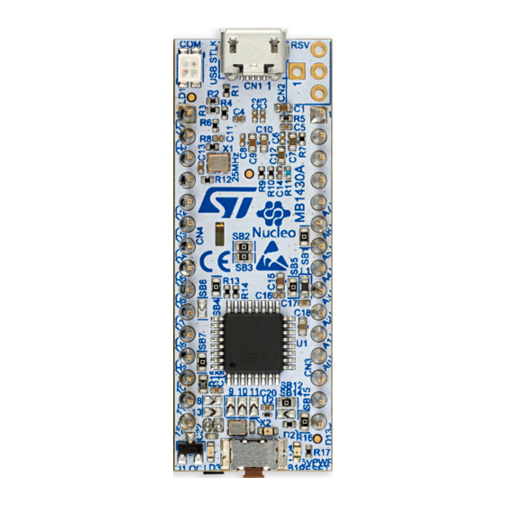
Figure 1.
NUCLEO-G431KB top view
Figure 2.
NUCLEO-G431KB bottom view
Pictures are not contractual.
UM2397 - Rev 2 - September 2019
www.st.com
For further information contact your local STMicroelectronics sales office.
Advertisement
Table of Contents

Related Manuals for ST STM32G4 Nucleo-32


Summary of Contents for ST STM32G4 Nucleo-32
-
Page 1: Figure 1. Nucleo-G431Kb Top View
Nano V3 connectivity provides easy means of expanding the functionality of the Nucleo open development platform with a wide choice of specialized shields. The STM32G4 Nucleo-32 board does not require any separate probe as it integrates the STLINK-V3E debugger/programmer. The STM32G4 Nucleo-32 board comes with the comprehensive free software libraries and examples available with the STM32CubeG4 MCU Package. -
Page 2: Features
– USB with Micro-B ® – ARDUINO Nano V3 expansion connector • Flexible power-supply options: ST-LINK USB V or external sources • On-board STLINK-V3E debugger/programmer with SWD connector: – USB re-enumeration capability: virtual COM port, mass storage, debug port •... -
Page 3: Ordering Information
Evaluation tools marked as “ES” or “E” are not yet qualified and therefore not ready to be used as reference design or in production. Any consequences deriving from such usage will not be at ST charge. In no event, ST will be liable for any customer usage of these engineering sample tools as reference design or in production. -
Page 4: Development Environment
STM32 Flash memory for easy demonstration of the device peripherals in standalone mode. The latest versions of the demonstration source code and associated documentation can be downloaded from www.st.com. UM2397 - Rev 2 page 4/30... -
Page 5: Conventions
UM2397 Conventions Conventions Table 3 provides the conventions used for the ON and OFF settings in the present document. Table 3. ON/OFF convention Convention Definition Jumper JPx ON Jumper fitted Jumper JPx OFF Jumper not fitted Jumper JPx [1-2] Jumper should be fitted between Pin 1 and Pin 2 Solder bridge SBx ON SBx connections closed by 0 Ω... -
Page 6: Quick Start
To power the board, connect the STM32G4 Nucleo-32 board to a PC with a USB cable (Type-A to Micro-B) through the USB connector CN1 of the board. Then, LED LD1 (COM) and green LED LD4 (5V_PWR) light up, green LED LD2 blinks. -
Page 7: Hardware Layout And Configuration
UM2397 Hardware layout and configuration Hardware layout and configuration The STM32G4 Nucleo-32 board is designed around the STM32 microcontrollers in a 32-pin UFQFPN package. Figure 3 shows the connections between the STM32 and its peripherals (STLINK-V3E, push button, LEDs, USB and Arduino Nano). -
Page 8: Pcb Layout
UM2397 PCB layout PCB layout Figure 4. Top layout STLINK-V3E Micro-B USB connector LD1 bicolor LED (COM) SWD connector (not fitted) X1 25 MHz oscillator U1 Main CPU (STM32G431KBT6) X2 24 MHz HSE crystal LD2 green LED (USER) LD4 green LED (5V_PWR) LD3 red LED (Overcurrent) B1 green RESET button UM2397 - Rev 2... -
Page 9: Figure 5. Bottom Layout
UM2397 PCB layout Figure 5. Bottom layout STLINK-V3E Micro-B USB connector U4 Common mode filter with ESD protection for USB U5 STM32F723IEK6 (STLINK-V3E MCU) ARDUINO Nano ® connector HW1 (2.54 mm jumper) on CN4 [4-5] U6 3V3_STLK regulator LD3985M33R 5V_USB_STLK regulator STMPS2151STR ARDUINO Nano... -
Page 10: Mechanical Drawing
UM2397 Mechanical drawing Mechanical drawing Figure 6. STM32G4 Nucleo 32 board mechanical drawing (in millimeter) 18.542 mm UM2397 - Rev 2 page 10/30... -
Page 11: Embedded Stlink-V3E
5 V power green LED LD4 (5V_PWR) 6.3.1 Drivers Before connecting the STM32G4 Nucleo-32 board to a Windows PC via USB, the user must install a driver for the STLINK-V3E (not required for Windows 10). It is available at the www.st.com website. -
Page 12: Power Supply
(AVDD) SB5 (ON) AVDD In case VIN, 5V or 3V3 is used to power the STM32G4 Nucleo-32 board, this power source must comply with the EN-60950-1: 2006+A11/2009 standard and must be Safety Extra Low Voltage (SELV) with limited power capability. -
Page 13: Table 5. External Power Sources: Vin (7 V - 12 V)
Over Current) is lit. The Nucleo board and its shield can be powered from ST-LINK USB connector CN1, but only ST-LINK circuit gets power before USB enumeration, because the host PC only provides 100 mA to the board at that time. -
Page 14: Debugging While Using Vin Or Ext As An External Power Supply
Debugging while using VIN or EXT as an external power supply When powered by VIN or 5V, it is still possible to use the ST-LINK for programming or debugging only, but it is mandatory to power the board first using VIN or EXT (either 3V3 or 5V), then to connect the USB cable to the PC. -
Page 15: Figure 9. Stm32G431Kb Nucleo-32 Board Clock Configuration
SB11 and SB8 OFF – SB13 OFF • HSE bypass configuration (from ST-LINK): The input clock is the ST-LINK MCO output. The frequency is fixed to 25 MHz, and connected to the PF0-OSC_IN of the STM32G4 microcontroller. The configuration must be: –... -
Page 16: Board Functions
The green LED indicates that the STM32G4 part is powered, and the 5 V power is available on CN3 pin 4. LD3 USB power fault (OC, overcurrent) LD3 indicates that the board power consumption on USB ST-LINK exceeds 500 mA. Therefore, the user must check the root cause of the overconsumption, and consequently (if needed) power the STM32G4 Nucleo-32 board with an external power supply. -
Page 17: Solder Bridges
UM2397 Solder bridges Solder bridges All the 16 solder bridges are located on the bottom layer of the STM32G4 Nucleo-32 board. Table 9. Solder bridge configuration Solder Solder bridge control State Description bridge (SB) T_VCP_TX is connected to STM32G4 I/O PA2. - Page 18 PF0-OSC_IN pin not connected to PF0 (ARDUINO Nano, CN4, pin 10) PF0-OSC_IN provided by 25 MHz ST-LINK MCO SB13 PF0-OSC_IN not provided by 25 MHz ST-LINK MCO 1. The default SB state is in bold. UM2397 - Rev 2 page 18/30...
-
Page 19: Board Connectors
UM2397 Board connectors Board connectors Several connectors are present on the STM32G4 Nucleo-32 board. STLINK-V3E USB Micro-B connector CN1 The USB socket CN1 connects the embedded STLINK-V3E to the PC for the programming and debugging purposes. Figure 10. USB Micro-B connector CN1 (front view) Table 10. -
Page 20: Figure 11. Arduino ® Connectors
UM2397 ARDUINO® Nano V3 connectors ® Figure 11. ARDUINO connectors ARDUINO Nano ARDUINO Nano ® ® connector connector ® The related pinout for ARDUINO connector appears in Figure 12 and is listed in Table UM2397 - Rev 2 page 20/30... -
Page 21: Figure 12. Arduino ® Connector Pinout
UM2397 ARDUINO® Nano V3 connectors ® Figure 12. ARDUINO connector pinout UM2397 - Rev 2 page 21/30... -
Page 22: Table 9. Solder Bridge Configuration
UM2397 ARDUINO® Nano V3 connectors ® Table 11. ARDUINO connector pinout STLINK-V3E MCU Connector Pin name Signal name Function number Power input Ground T_NRST T_NRST PG10_NRST RESET 5V input/output ARD_A7 ADC1_IN3 ARD_A6 ADC2_IN4 ADC2_IN3 ARD_A5 PA15 I2C1_SCL ADC2_IN13 ARD_A4 I2C1_SDA ARD_A3 ADC2_IN17 ARD_A2... -
Page 23: Stm32G4 Nucleo-32 I/O Assignment
UM2397 STM32G4 Nucleo-32 I/O assignment STM32G4 Nucleo-32 I/O assignment Table 12. Nucleo-32 I/O assignment Pin name Signal or label Main feature / optional feature / (SB) VDD voltage supply PF0-OSC_IN PF0-OSC_IN HSE CLK input / IO PF1-OSC_OUT PF1-OSC_OUT HSE CLK output / IO... -
Page 24: Federal Communications Commission (Fcc) And Industry Canada (Ic) Compliance
UM2397 Federal Communications Commission (FCC) and Industry Canada (IC) Compliance Statements Federal Communications Commission (FCC) and Industry Canada (IC) Compliance Statements FCC Compliance Statement Part 15.19 This device complies with Part 15 of the FCC Rules. Operation is subject to the following two conditions: (1) this device may not cause harmful interference, and (2) this device must accept any interference received, including interference that may cause undesired operation. -
Page 25: Revision History
UM2397 Revision history Table 13. Document revision history Date Version Changes 17-May-2019 Initial release. 04-Sep-2019 ® Updated: Table 9 and ARDUINO registered trademark. UM2397 - Rev 2 page 25/30... -
Page 26: Table Of Contents
UM2397 Contents Contents Features................2 Ordering information . - Page 27 STM32G4 Nucleo-32 I/O assignment ........
-
Page 28: List Of Tables
UM2397 List of tables List of tables Table 1. Ordering information..............3 Table 2. -
Page 29: List Of Figures
STM32G4 Nucleo-32 board power tree ........ - Page 30 ST’s terms and conditions of sale in place at the time of order acknowledgement. Purchasers are solely responsible for the choice, selection, and use of ST products and ST assumes no liability for application assistance or the design of Purchasers’...
Need help?
Do you have a question about the STM32G4 Nucleo-32 and is the answer not in the manual?
Questions and answers